Used TEL / TOKYO ELECTRON P-12XLm #293804668 for sale
URL successfully copied!
Tap to zoom
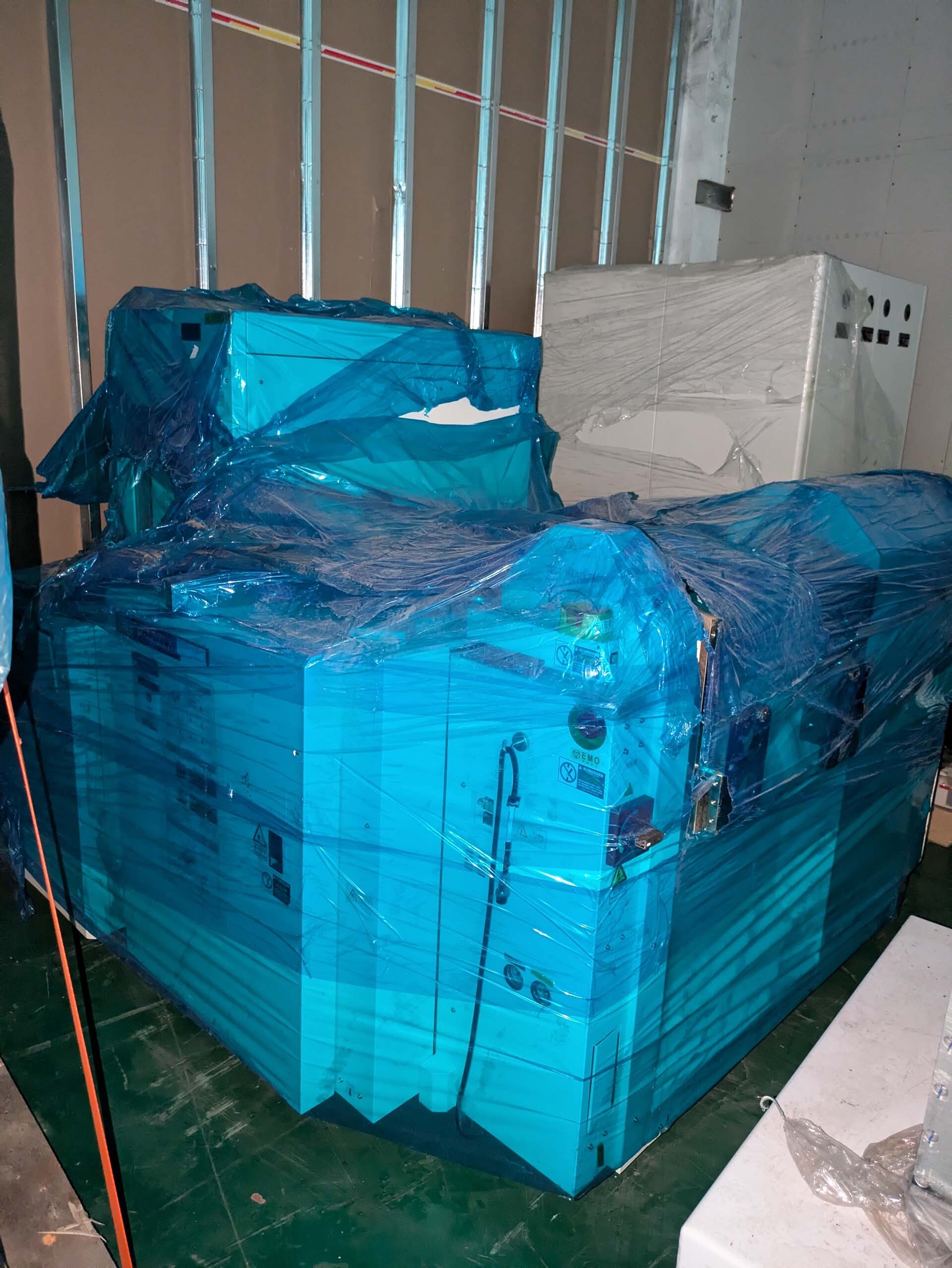

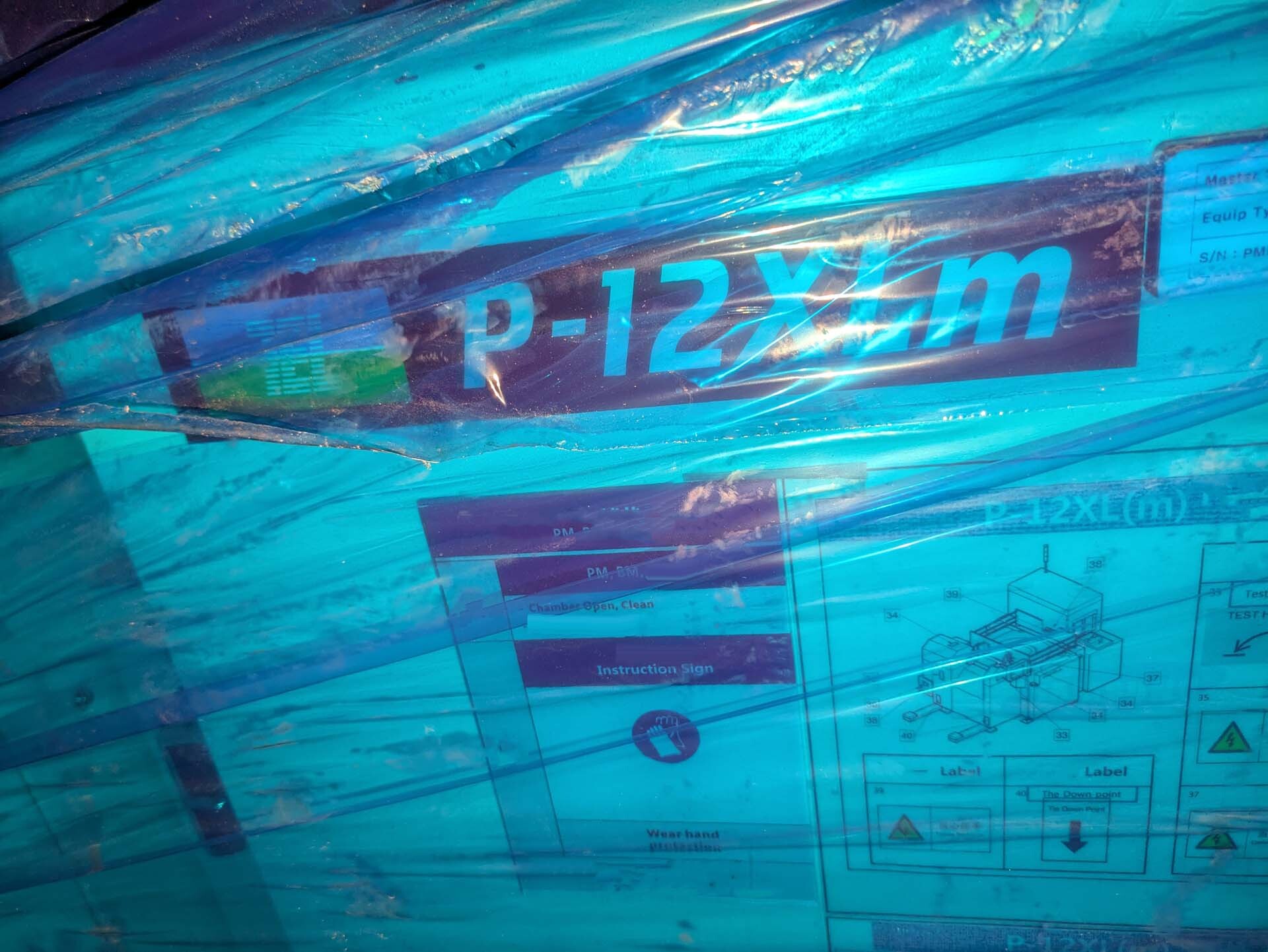
TEL / TOKYO ELECTRON P-12XLm is a wafer prober designed to be used with large wafers up to 300 mm in diameter. It utilizes TEL Prober Control Equipment (PCS) technology to provide accurate and highly stable wafer probing performance. This wafer prober was created to analyze wafers and their constituent components with high accuracy and speed, and to facilitate the observation of their physical and electrical characteristics. TEL P12XLM utilizes an advanced broad-range, dual-sensor system which is designed to achieve ultra-accurate positioning and high-speed mapping. The dual-sensor unit features a high-accuracy optical machine and a high-speed capacitive sensing tool. The optical asset measures wafer position with a range of 0.3μm and offers a maximum wafer repeatability of 0.15μm. The capacitive model senses the wafer position with a range of 0.05μm and offers a repeatability of 0.02μm. Together, the two sensing systems provide a total range of 0.25μm and accuracy of 0.08μm. TOKYO ELECTRON P 12 XLM also features advanced auto-leveling and leveling control capabilities which provide accurate and efficient wafer probing. A wafer bin handling equipment also allows for pre-alignment of wafers prior to probing as well as efficient wafer unloading/loading. In addition, P-12 XLM offers a broad range of metrology options, including laser microscope and OBIRCH clustering capabilities. The OBIRCH clustering capability allows a high degree of accuracy and speed when mapping physical defects related to the parameters of topography, such as height and incident angle. P 12 XLM is built with an open architecture design, which allows for a wide variety of control and measurement peripherals to be incorporated into the system, including sources, detectors, testers, and various analytical tools. This ensures a high degree of flexibility to adapt to various production environments. Overall, P-12XLm is an advanced, accurate, and highly adaptable wafer prober designed for large wafers. It utilizes advanced sensing and auto-leveling technology, as well as providing a broad range of metrology options, to facilitate the efficient analysis of wafers and their constituent components.
There are no reviews yet