Used TEL / TOKYO ELECTRON P-8 #293620443 for sale
URL successfully copied!
Tap to zoom
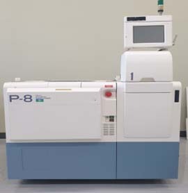




ID: 293620443
Wafer Size: 8"
Vintage: 1996
Prober, 8"
OS: Gzz00-R014.08QH
CPU Type: VIP3A
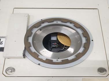
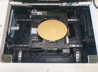
Hot gold chuck
Vacuum: ≤-50 kPa
Main air / Vac hose size: 6Ø
Top loader
Bernoulli and pad sub chuck
Chuck air blower
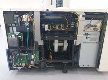
Solenoid block
Control board
OCR COGNEX insight 1700
Air pressure: 0.45 MPa - 0.7 MPa
SCSIHSD: 70-80% Increased speed
Memory: 8G / 16G SD Card
SCSI Interface
Power: 5V DC
Power supply: 200-240 V, 50-60 Hz, Single phase, 7.5 Amps
1996 vintage.
TEL / TOKYO ELECTRON P-8 is a prober for the analysis and testing of electronic components and devices on a semiconductor wafer. The device offers customers the opportunity to quickly, accurately and reliably analyze a variety of electronic components and devices. TEL P8 employs advanced optics and robotics to extract a wide range of data from the electronic components and devices. The device features a high-definition auto focus camera, which provides the user with resolution and clarity down to submicron levels. Additionally, TOKYO ELECTRON P 8 has a fully automated motorized stage that is capable of high speed scanning and submicron positioning accuracy. TOKYO ELECTRON P8 utilizes an advanced optical system that incorporates an automated zoom lensbfor high-precision surface measurements of the devices under test. By utilizing high-resolution digital color sensors and mechanical positioning, P8 can precisely image and focus on tight spots of a device's micro structure. TEL P 8 also has the capabilities to measure contact resistance, leakage current, and devices threshold voltages. The automated stage in TEL / TOKYO ELECTRON P8 is capable of scanning and positioning on semiconductor wafers at high speeds and with submicron accuracy. The stage also supports an off-the-shelf infrared alignment system for absolute accuracy on multiple and repeatable wafers. P-8 also comes with an integrated software suite for both intermediate and expert users. The software suite has features such as an intuitive graphical user interface, automated data analysis, network configuration and customization of recipes. P 8 is an advanced, cutting-edge prober for the electronic device testing and analysis market. It incorporates a variety of advanced optics and robotics for measuring, imaging, and analyzing devices on semiconductor wafers. The automated stage, advanced optics, and intuitive software suite all combine to offer users a simple and powerful tool for analyzing the characteristics and performance of semiconductor devices.
There are no reviews yet
