Used TEL / TOKYO ELECTRON P-8 #293742044 for sale
URL successfully copied!
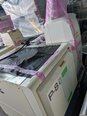
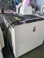
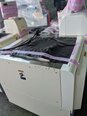
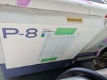
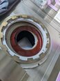
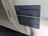
Tap to zoom
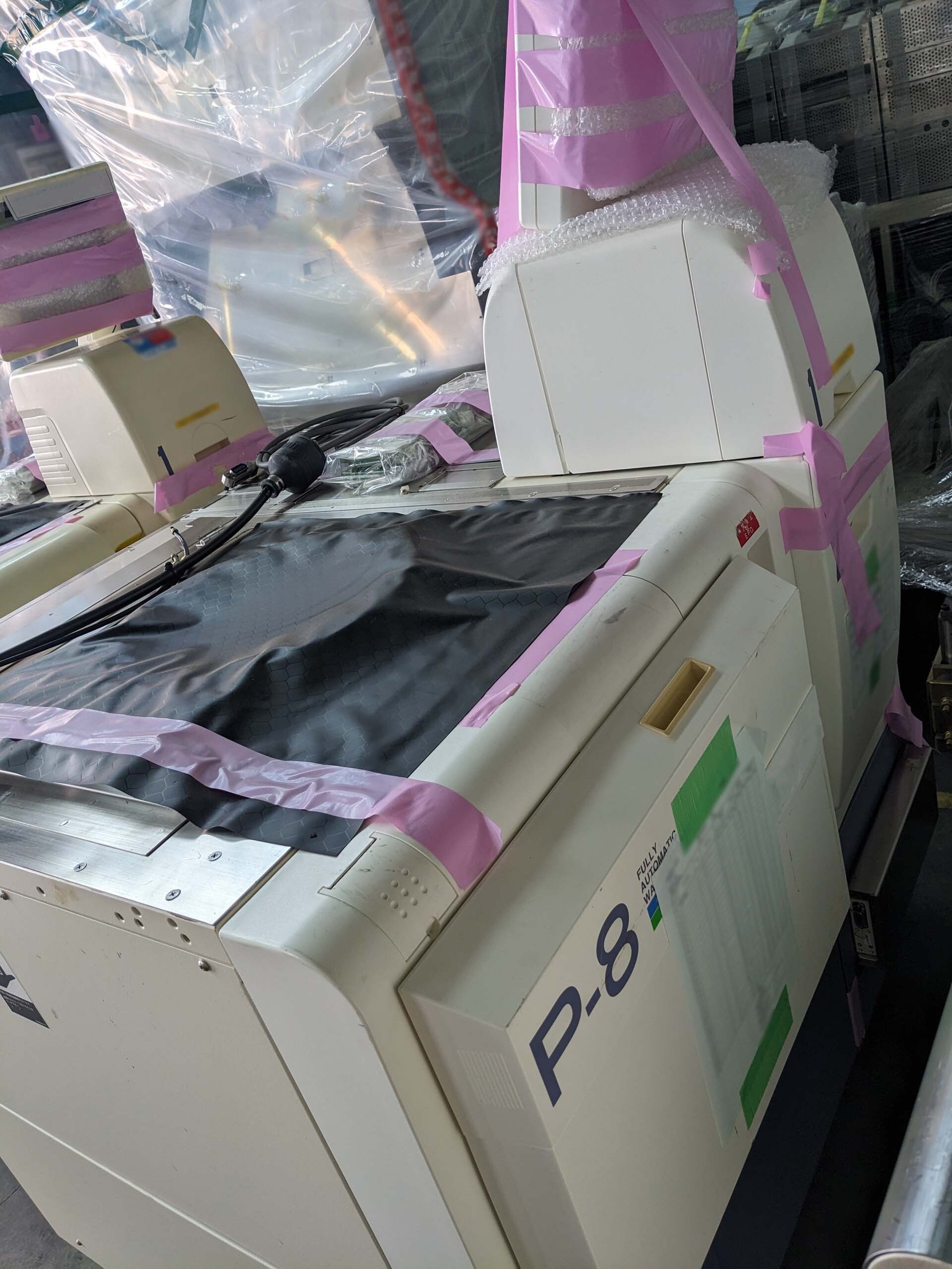

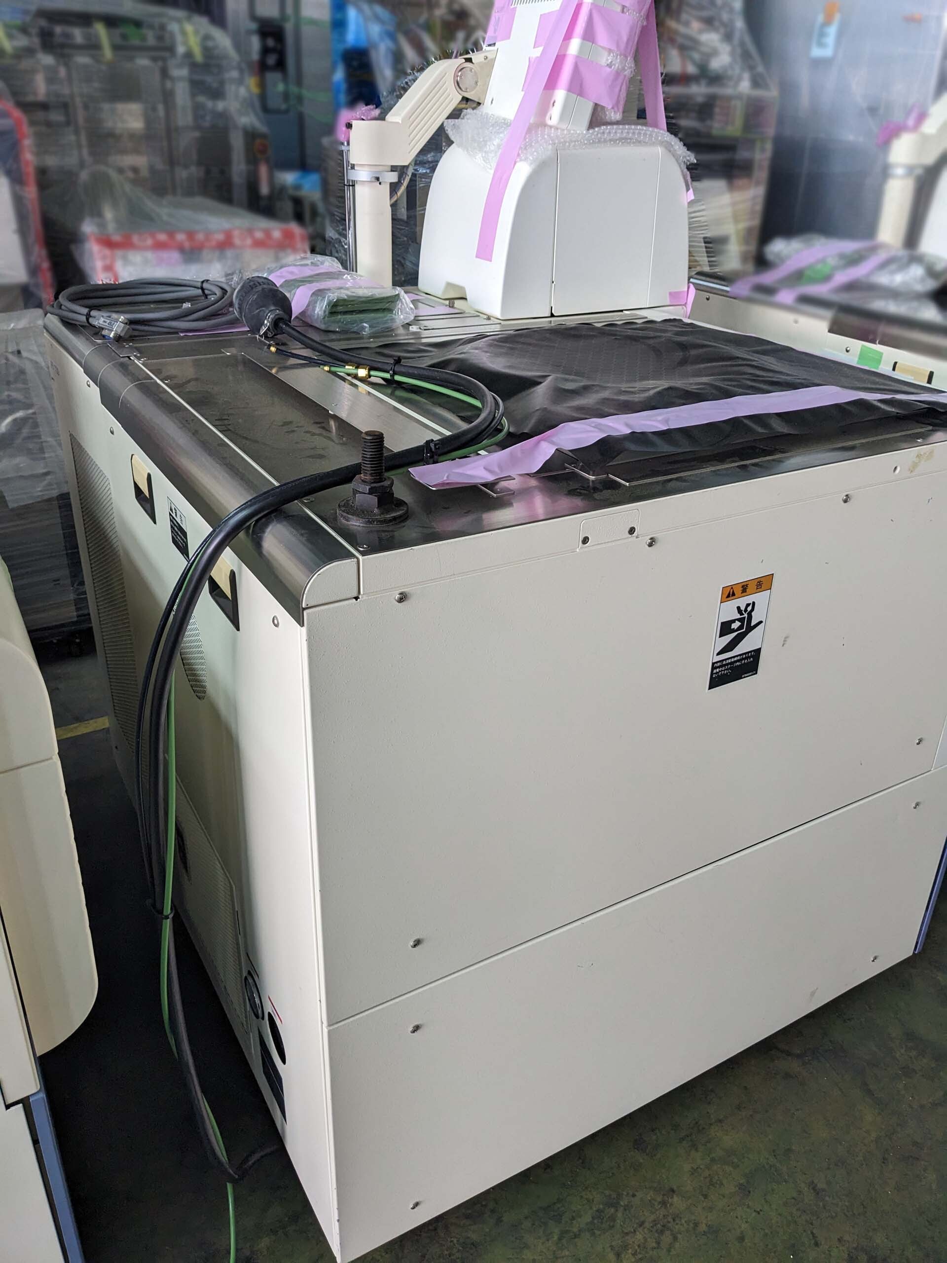
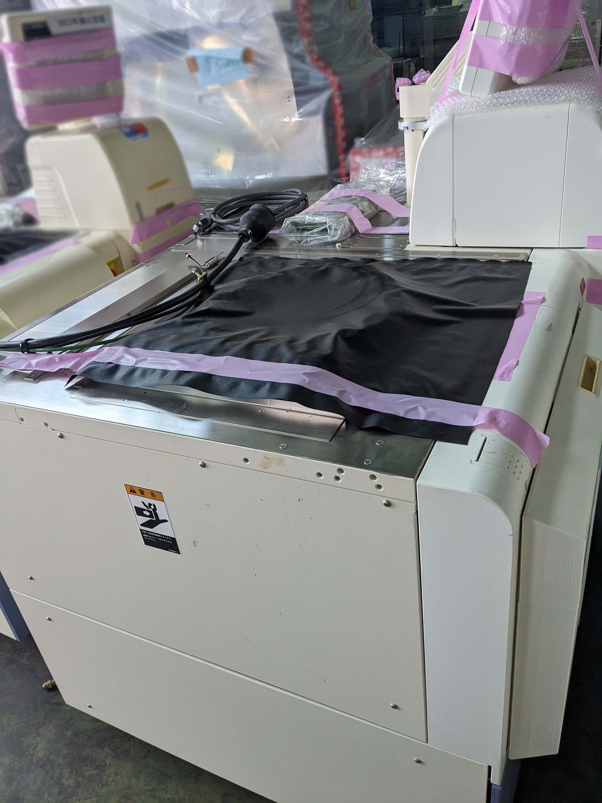
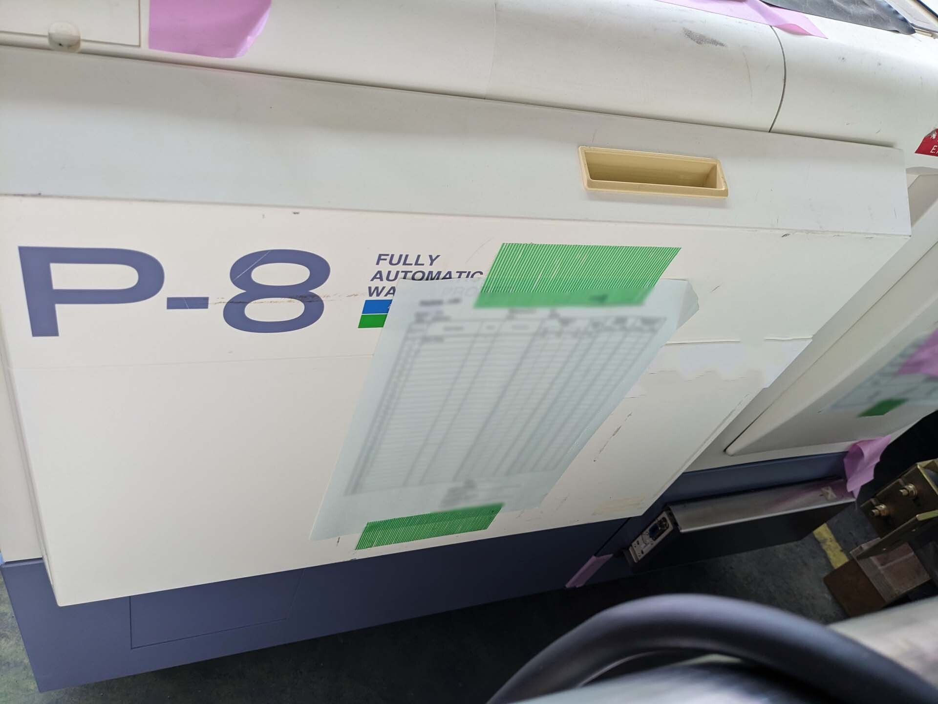
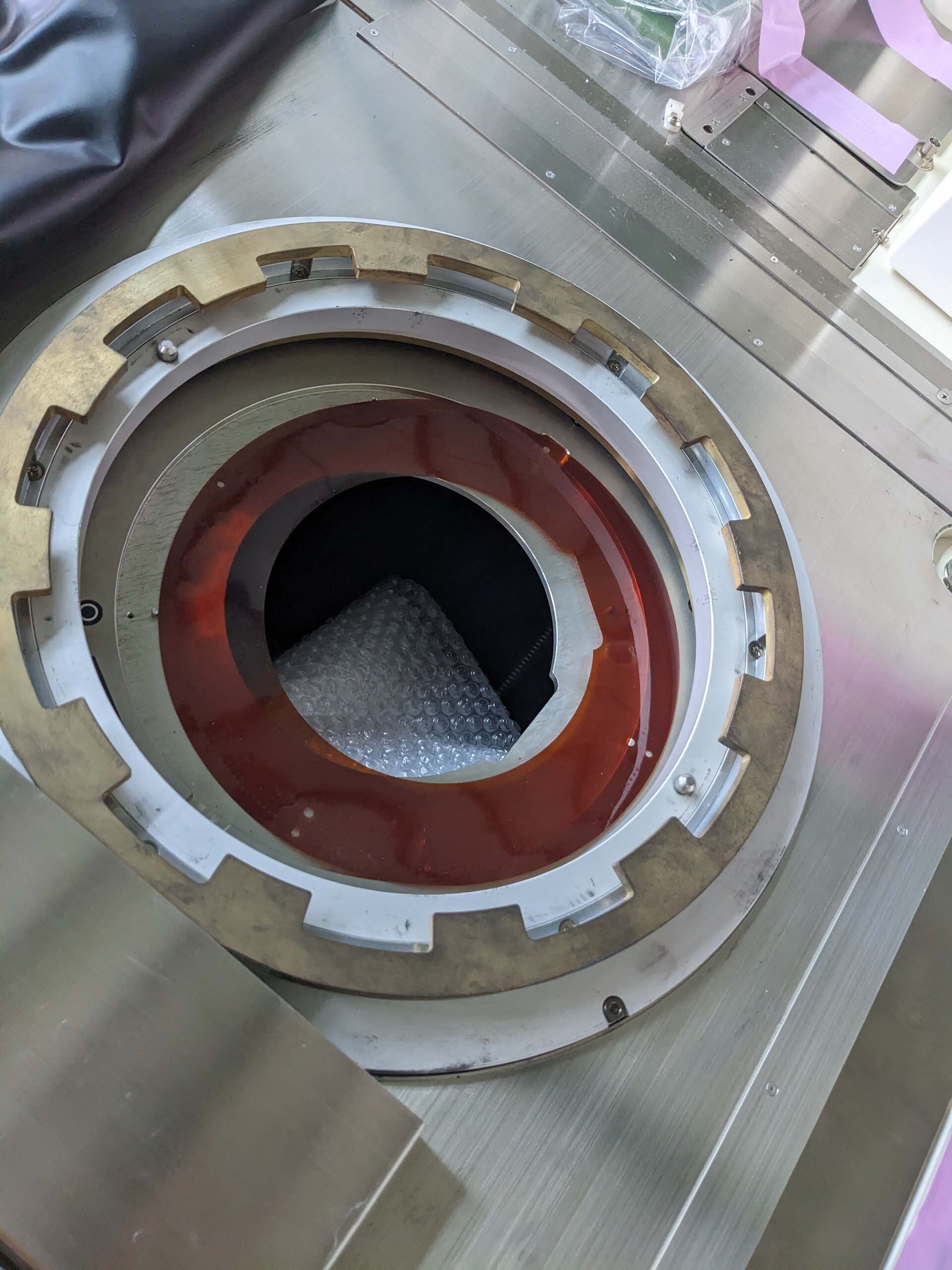
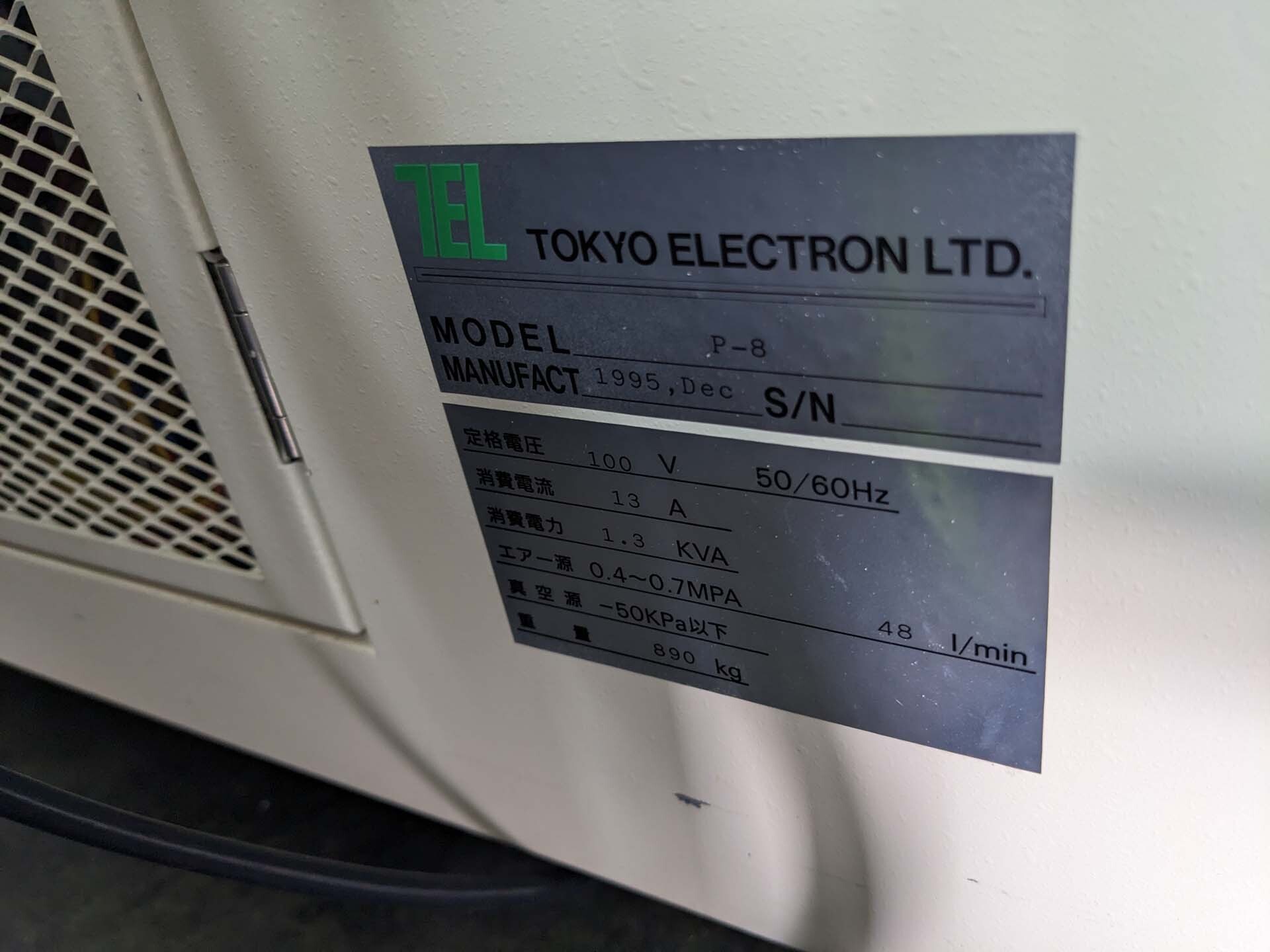
ID: 293742044
Wafer Size: 8"
Vintage: 1995
Prober, 8"
Nickel plated chuck
Hot chuck temperature: 40°-150°C
Tester: GPIB
CPU Type: IP/DP
No ethernet
No OCR Camera
No inker
1995 vintage.
TEL / TOKYO ELECTRON P-8 prober is an advanced semiconductor probing equipment designed to enable precise probing of the smallest device structures on the market. The full automated wafer prober is designed to perform both contactless die-mode probing and single-site contact probing with a maximum die area of 155 mm x 155 mm. TEL P8 provides high accuracy through the use of an advanced optical alignment system and a dual-stage precision X/Y stage. The instrument is comprised of two main components, the prober itself and the probing arm. The prober base contains a precision X/Y air bearing stage that is driven by a stepper motor, a mounting base for the prober arm, and a scanner for contactless die-mode probing. The prober arm features a low-noise flexure-mounting unit for precise motion control. The arm has a hand-held gripper for manual die alignment, as well as robotic end-effectors for automated die alignment. TOKYO ELECTRON P 8 is designed with a wide range of configurable options that can be adjusted according to the specific application. The prober can be equipped with both manual and semi-automatic aligners to achieve accurate die-level Alignment, while its two-stage X/Y precision stage allows users to easily correct sample misalignments. The prober also offers options for low-force contact probing (LFCT) and vacuum-sealing technology for better die-level probing. TEL / TOKYO ELECTRON P 8 prober is compatible with a variety of probing systems, including high-voltage and parametric probing systems. The instrument is also designed to support automated wafer-level handling applications such as wafer level burn-in, when used with its robot handling machine. The prober is capable of producing high-resolution images of samples down to 100 nm with its contactless die-mode probing. Additionally, it supports both real-time statistical feedback and temperature control, allowing users to maintain sample integrity in highly regulated semiconductor manufacturing environments. TEL / TOKYO ELECTRON P8 prober provides advanced capabilities for automated probing and other semiconductor testing applications. It is an essential instrument for the most advanced semiconductor manufacturing processes, allowing precise probing on the smallest device structures. The robust design ensures outstanding operation and long-term reliability, while the advanced technology provides high accuracy and precise results.
There are no reviews yet