Used TEL / TOKYO ELECTRON P-8 #293754653 for sale
URL successfully copied!
Tap to zoom
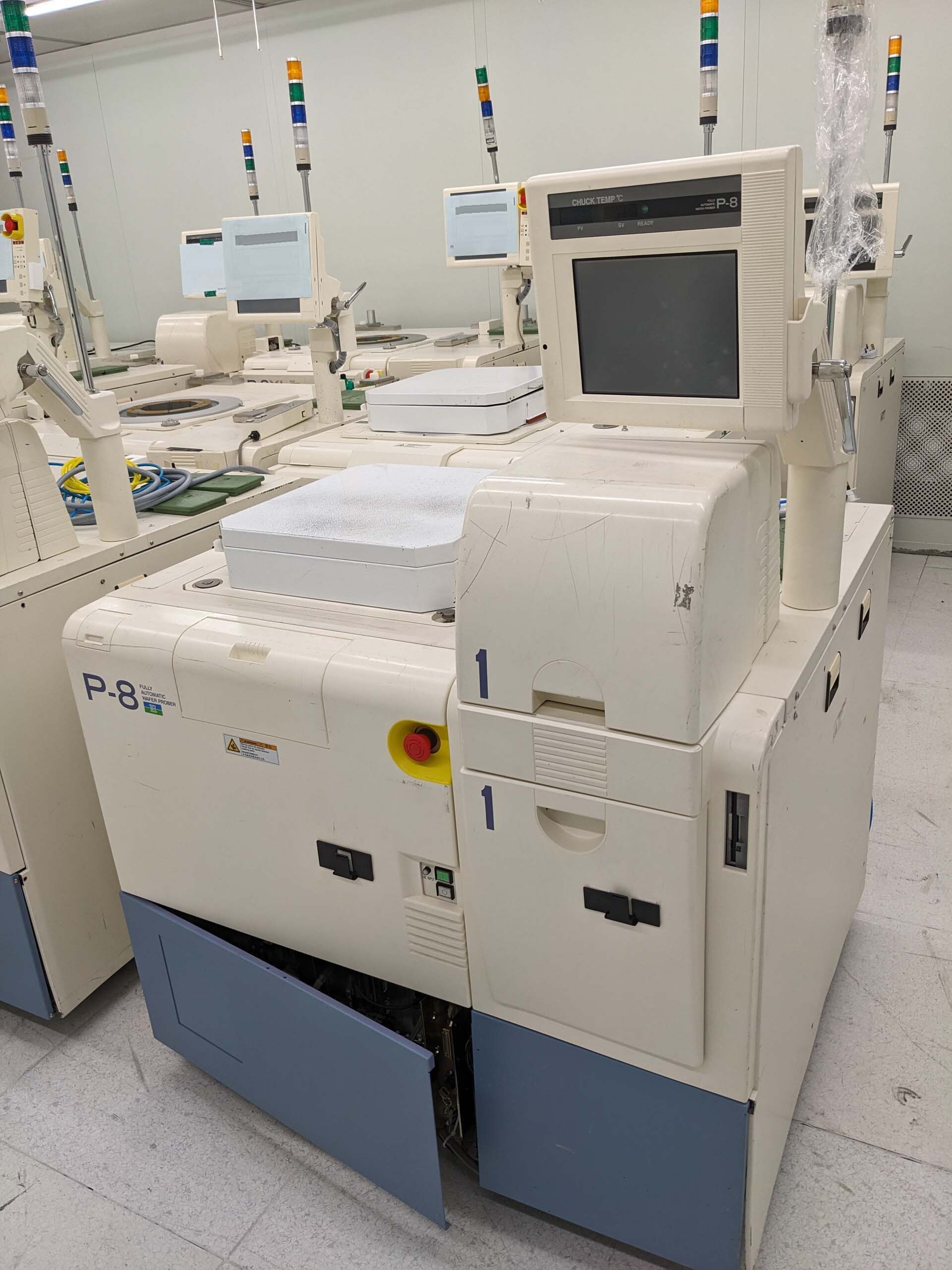

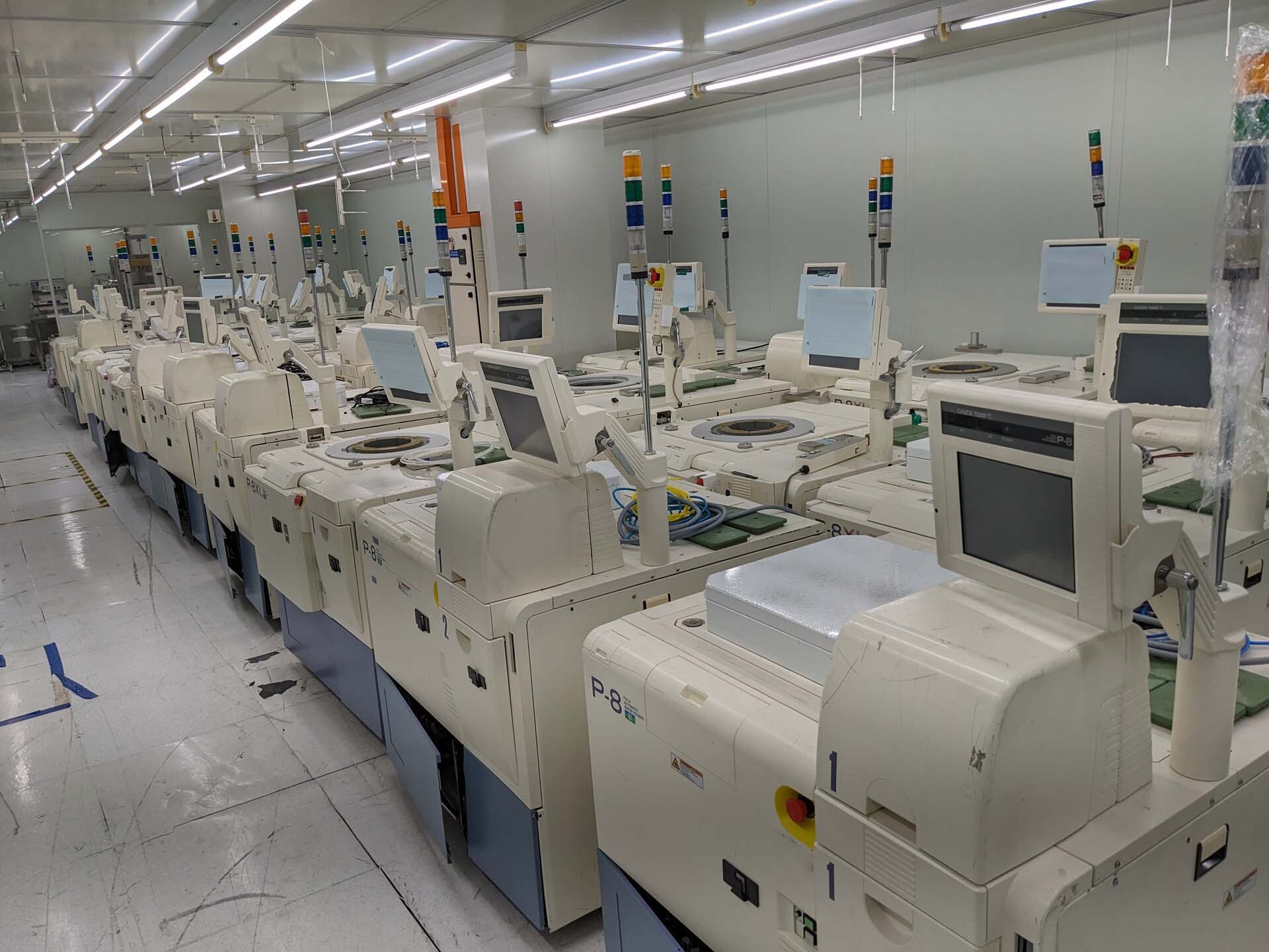
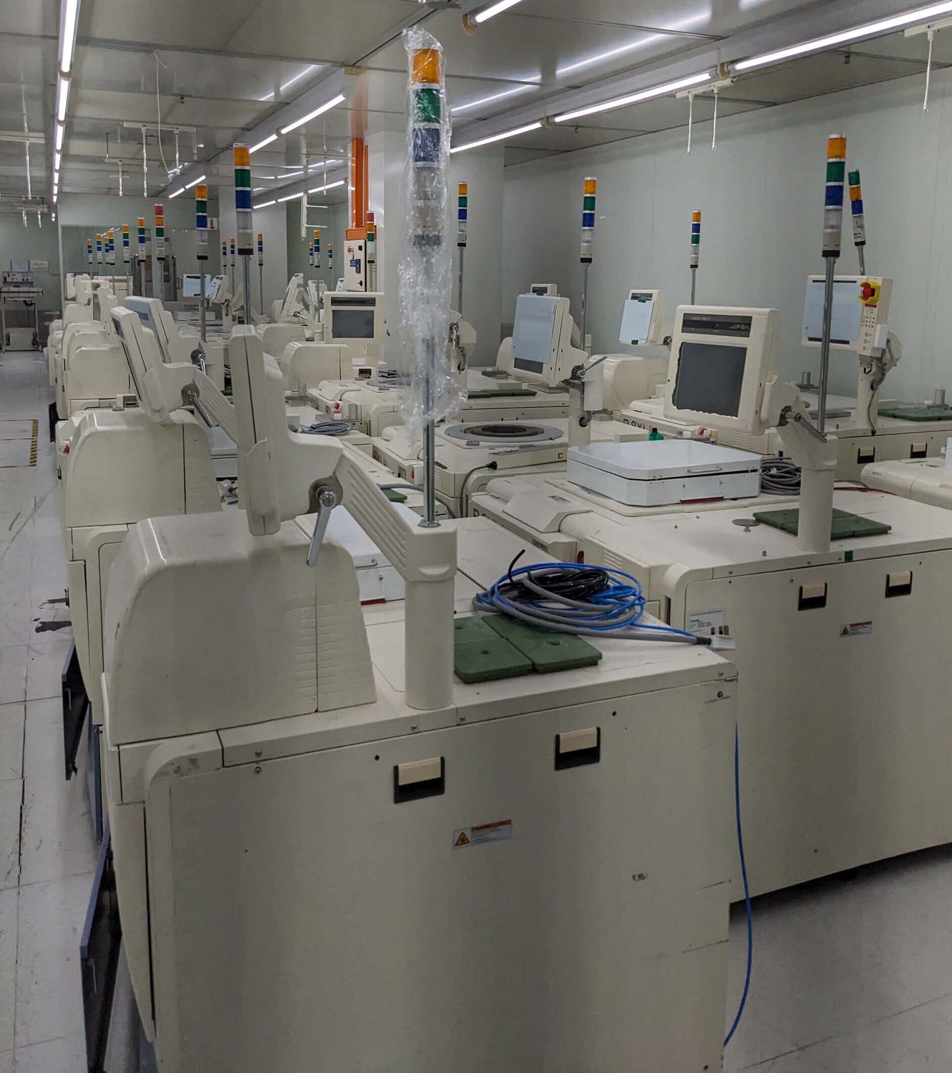
TEL / TOKYO ELECTRON P-8 is an advanced prober designed for wafer joining, inspection, and failure analysis. It features an intuitive user interface and an advanced vision equipment that make it easy to operate and allows for precise probing. TEL P8 is a highly configurable piece of equipment, capable of performing contact probing, field emission, focused ion beam inspection, low-energy ion beam mapping, and thermal imaging. The prober has the ability to immunize and optimize the settings for each sample type ensuring a precisely optimized probing result. It uses a stylus of less than 75 nanometers diameter and allows for the analysis of samples up to 20×20 mm in size. The vision system in TOKYO ELECTRON P 8 is equipped with a sophisticated focal point setting which adjusts the size and location of the probe field in order to get the most accurate results. The range of settings allows for adjustment depending on the size and shape of the samples being tested. In addition, the prober provides an improved Z-shift capability and enhanced low-voltage probing. To ensure reliability and accuracy, the prober is furnished with components of the highest quality. The wafer joining process has become more reliable with a tolerance limit of +/- 1 micron. Moreover, the automated alignment unit allows for fast and accurate alignment. Finally, the high repeatability ensures that the same job can be done multiple times to the same result. The machine also has a powerful vision machine that allows for a wide range of automatic inspection capabilities. It is equipped with a wide array of functions that can detect surface anomalies, evaluate micro defects, or perform high-resolution imaging. Designed with a low thermal budget, P-8 is able to maintain temperature consistency with only minor temperature variations. This is especially useful when conducting temperature-sensitive testing. Overall, P8 is a reliable prober tool suitable for a wide range of wafer joining, inspection, and failure analysis applications. With its intuitive user interface, advanced vision asset, and reliable probing capabilities, it is an excellent choice for any laboratory seeking an efficient, reliable, and powerful prober.
There are no reviews yet