Used TEL / TOKYO ELECTRON P-8 #9361265 for sale
URL successfully copied!
Tap to zoom


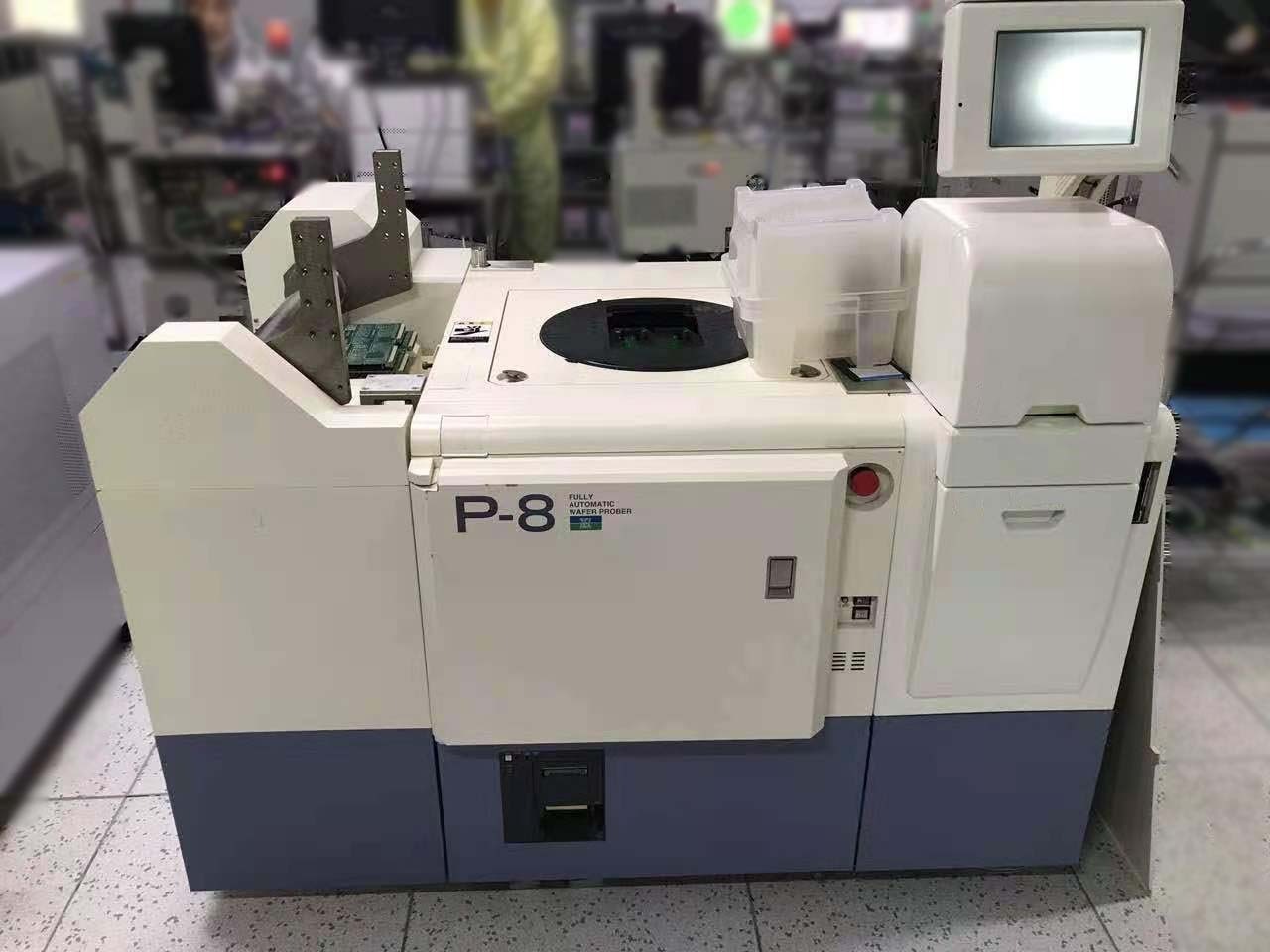
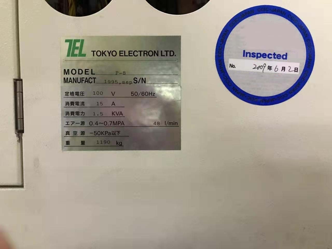
TEL / TOKYO ELECTRON P-8 is an automated wafer prober designed to precisely measure the electrical properties of semiconductor devices. The prober is designed to maximize throughput in order to provide accurate, repeatable and reliable results. The equipment is composed of a tray-loading mechanism, a wafer transport module, a prober, alignment tooling in the form of a laser, as well as an optional probe card caddy. The tray-loading mechanism allows users to quickly and easily load multiple wafers onto the prober. The wafer transport module is responsible for transporting the wafers from the tray to the prober and back. This is done using a vacuum-controlled transport system and a robotic arm. The laser alignment tooling is specifically designed to align wafers on the prober. This ensures that the probes of the prober make contact with the device to be tested in the optimum location for reliable testing. The prober itself is the core component of TEL P8 unit. It has a modular design, allowing it to be integrated into other processes such as back-end testing. It can be used to measure electrical properties of semiconductor devices such as current leakage, breakdown voltage, and gate capacitance. The open platform prober has the ability to accommodate various panel sizes to allow for the testing of specialty devices. It also has a high speed probe positioning machine, allowing for testing in a variety of configurations. The optional probe card caddy enables compatibility with multiple probe card types. This enables users to perform tests with different types of measurement tools. TOKYO ELECTRON P 8 tool can also be integrated with a vision asset, thereby allowing users to take advantage of visual inspection and wafer mapping. P8 is an advanced automated wafer prober capable of providing reliable, repeatable and accurate testing results. The model is composed of a tray-loading mechanism, a wafer transport module, a prober, laser alignment tooling, and an optional probe card caddy. The modular design makes the prober compatible with other processes and can accommodate multiple panel sizes. The high-speed probe positioning equipment makes the system suitable for a variety of testing configurations and inspection purposes. Finally, the unit is user friendly and easy to operate, offering users the ability to get reliable results quickly and efficiently.
There are no reviews yet

