Used TEL / TOKYO ELECTRON P-8XL #293827263 for sale
URL successfully copied!
Tap to zoom
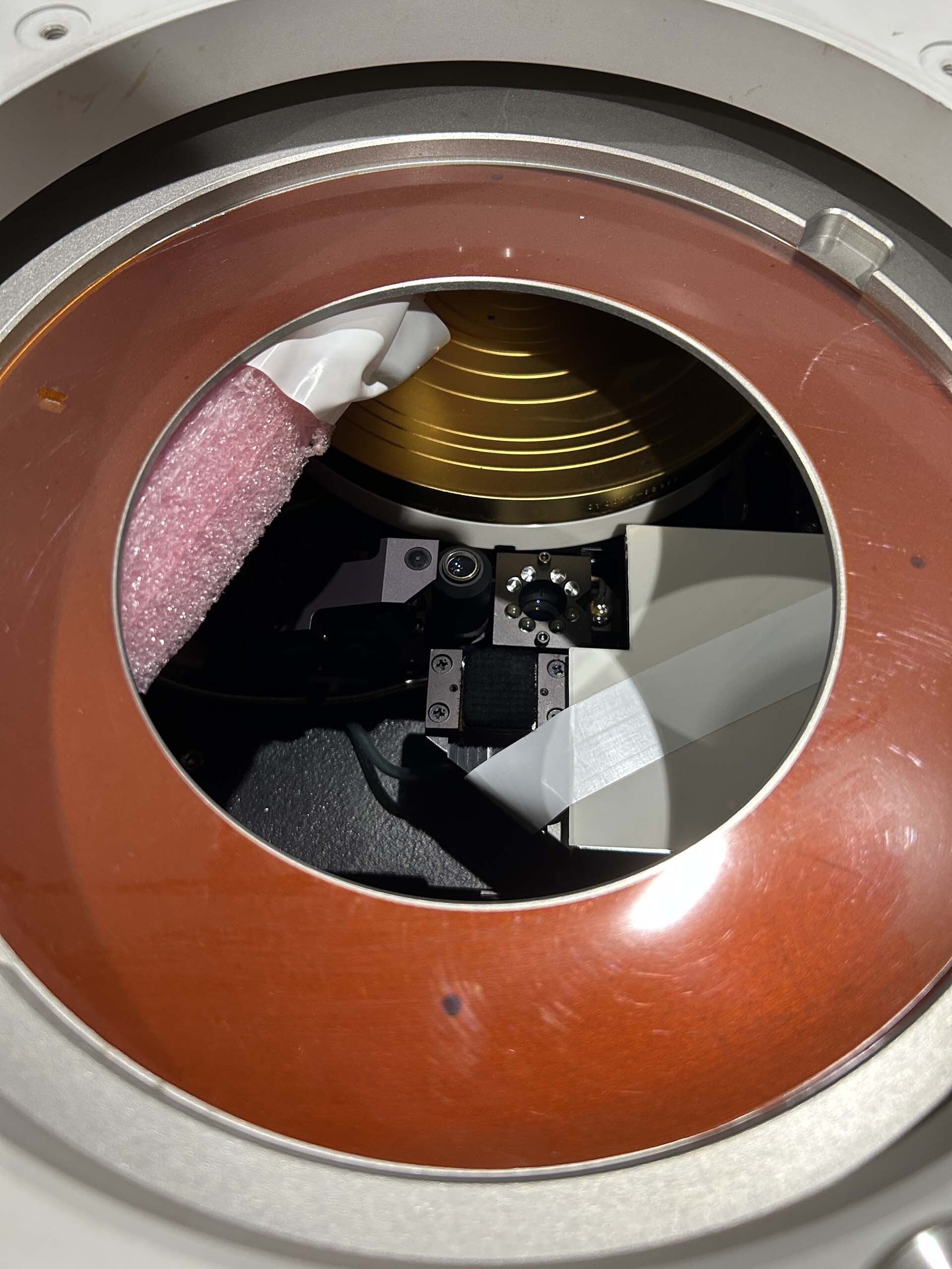

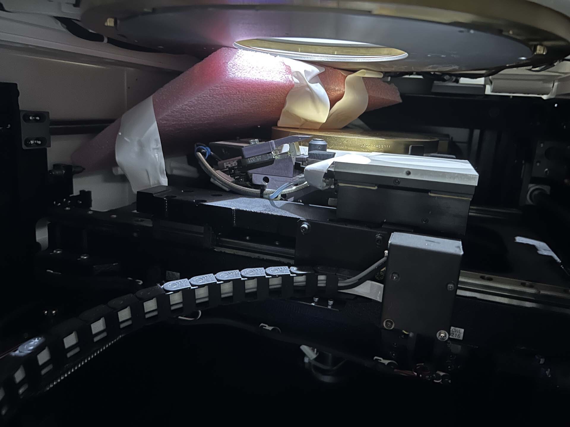
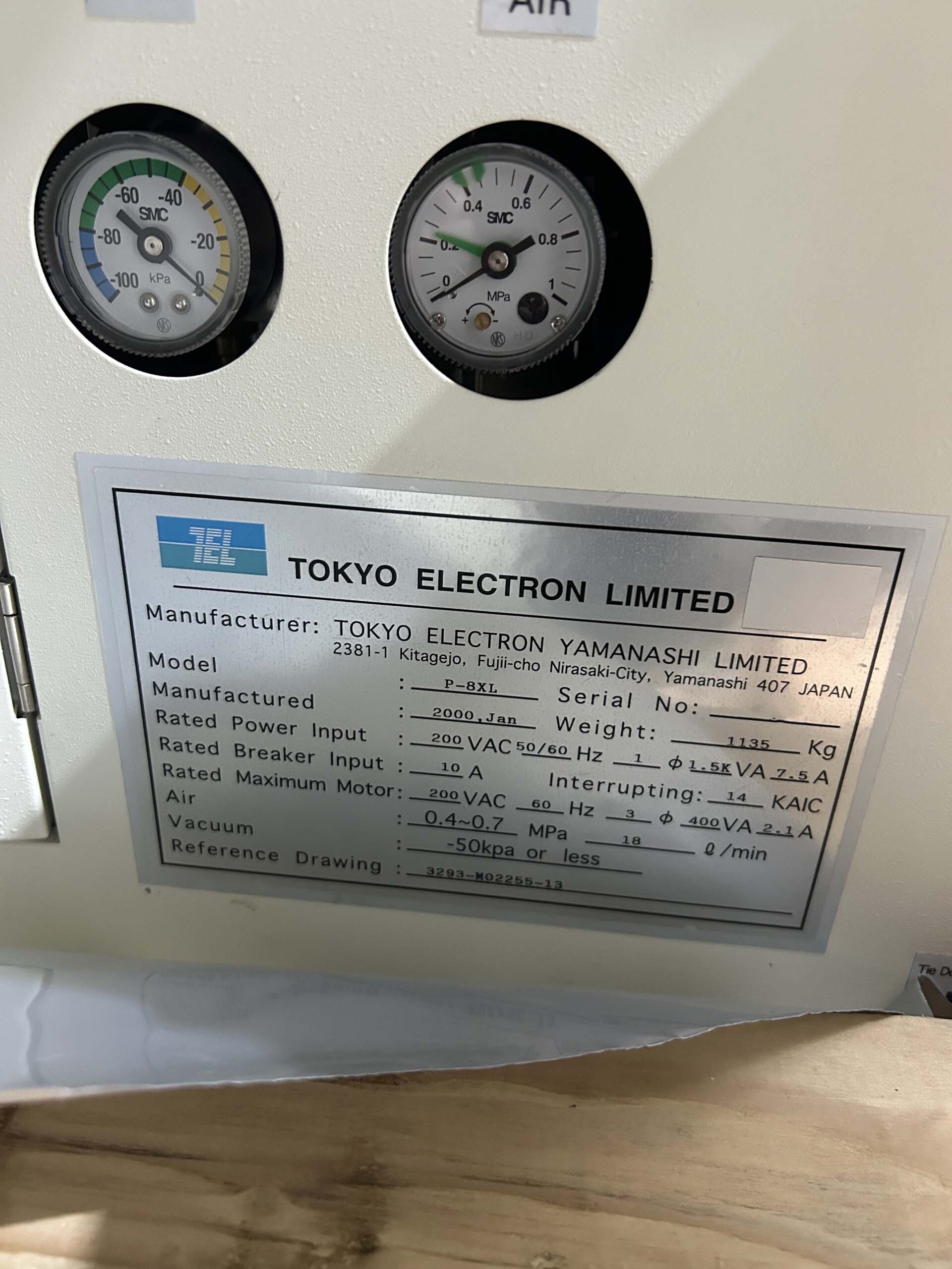
TEL / TOKYO ELECTRON P-8XL Prober is a fully automated, high precision wafer probing equipment designed for the testing and measurement of integrated circuits and components on semiconductor wafers. The versatile TEL P8XL Prober offers a wide range of capabilities, including automatic alignment and focus control, precise probe card alignment and motion control, and high-precision automatic probing of up to eight lanes in parallel, all of which can be easily configured to fit a number of customer requirements. TOKYO ELECTRON P8-XL Prober is designed to be highly accurate and provide repeatable results. It uses a patented Wafer Indexing System (WIS) that ensures the same positioning and alignment of the wafer across all its steps in the testing process, as well as an automatic tool centering unit. This ensures proper alignment and accuracy when transferring data between the wafer and the probe card, ensuring data accuracy and repeatability. TOKYO ELECTRON P-8XL Prober is designed to be user-friendly, with a large and intuitive touchscreen GUI and easy access to all its components. In addition, it offers various levels of control over its probing capability, from basic macros to advanced algorithms, making it easy to customize its performance for a wide range of needs. Furthermore, multiple processes can be run simultaneously, helping to maximize productivity. In addition to highly accurate wafer probing, TEL P-8 XL Prober also offers post-probing analysis capabilities. It is capable of performing gate and contact leakage testing, transistor measurements, and pattern comparisons, and can be linked to an optional automatic defect review (ADR) machine. This allows for a reliable trace mapping and defect classification, making it an ideal choice for complex testing applications. Overall, P-8XL Prober offers a high level of efficiency and accuracy in wafer probing and testing. Its automatic alignment and focus control, customizable probing algorithms, and post-probing defect analysis make it an excellent choice for use in a variety of semiconductor production environments.
There are no reviews yet