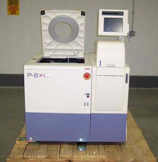
Used TEL / TOKYO ELECTRON P-8XL #9193119 for sale
URL successfully copied!
Tap to zoom


ID: 9193119
Wafer Size: 5"-8"
Fully automatic wafer prober, 5"-8"
Voltage hot chuck: Ni Hi
WAPP
Probe card cleaning plate & brush
Semi automatic card changer
Indexer slide loader
Wafer prealigner
Wafer Table
Media handler: Wafer
Boards:
GPIB
VIP3A
CPU
Interface: Credence quartet tester
PTPA Accuracy: +/- 4.0µm
PTPA Z Accuracy: +/- 5.0µm
Inspections:
Ink dot
Probe mark
Power: 220 V
Frequency: 50/60 Hz
Current: 7.5 A.
TEL / TOKYO ELECTRON P-8XL prober is a highly advanced laser-based wafer contact prober capable of probing stringent contact requirements on advanced wafer technologies. It is designed for accuracy and repeatability, and uses a compact optical deflection equipment which allows for precision scanning with accurate motion control for rapid wafer testing. With its unique alignment system, TEL P8XL prober can automatically align any target sites and perform accurate and repeatable testing of advanced wafer technologies. It has a Wafer Acceptance Rate of over 98%, utilizing a laser-based positioning unit to precisely align the Wafer to the probes, thereby minimizing measurement errors. TOKYO ELECTRON P8-XL is also capable of probing and analyzing Wafers featuring octagonal-shaped bumps and provides users with both high-accuracy synchronization scanning for repeatable measurements and low-latency reticle scanning for multiple-contact probing. TEL / TOKYO ELECTRON P8-XL also features a high-resolution dual-numbered color LCD display for viewing sample images, statistics, and measured data in either a native or a block test mode. Its Atomic Level Pre-Alignment Technology (A-L-PAT) uses multiple cameras, both on-board and off-board, to ensure precise alignment and calibration of the WAFER and to maximize accuracy. On-board die position can then be monitored and controlled for up to 6 axes including X, Y, tilt-angle, laser power, and TFR deviation correction. P8XL uses a dual-beam scanning machine featuring both a laser and a micrometer positioner. The laser positioner is used for probing and imaging the Wafer, while the micrometer is used for positioning the probes and loading the Wafer onto the stage. In addition, P-8XL can be fitted with a special contact probe designed to help measure large-die semiconductor chips and to map the wafer surface precisely. TEL P-8XL Prober has a wide range of capabilities and offers superior performance, accuracy, and repeatability for wafer probing, imaging, and measurement. With its advanced features and high-quality components, TEL / TOKYO ELECTRON P 8 XL is capable of meeting the most stringent testing requirements and offers users the highest performance and accuracy available in wafer probers today.
There are no reviews yet