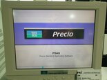
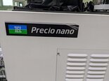
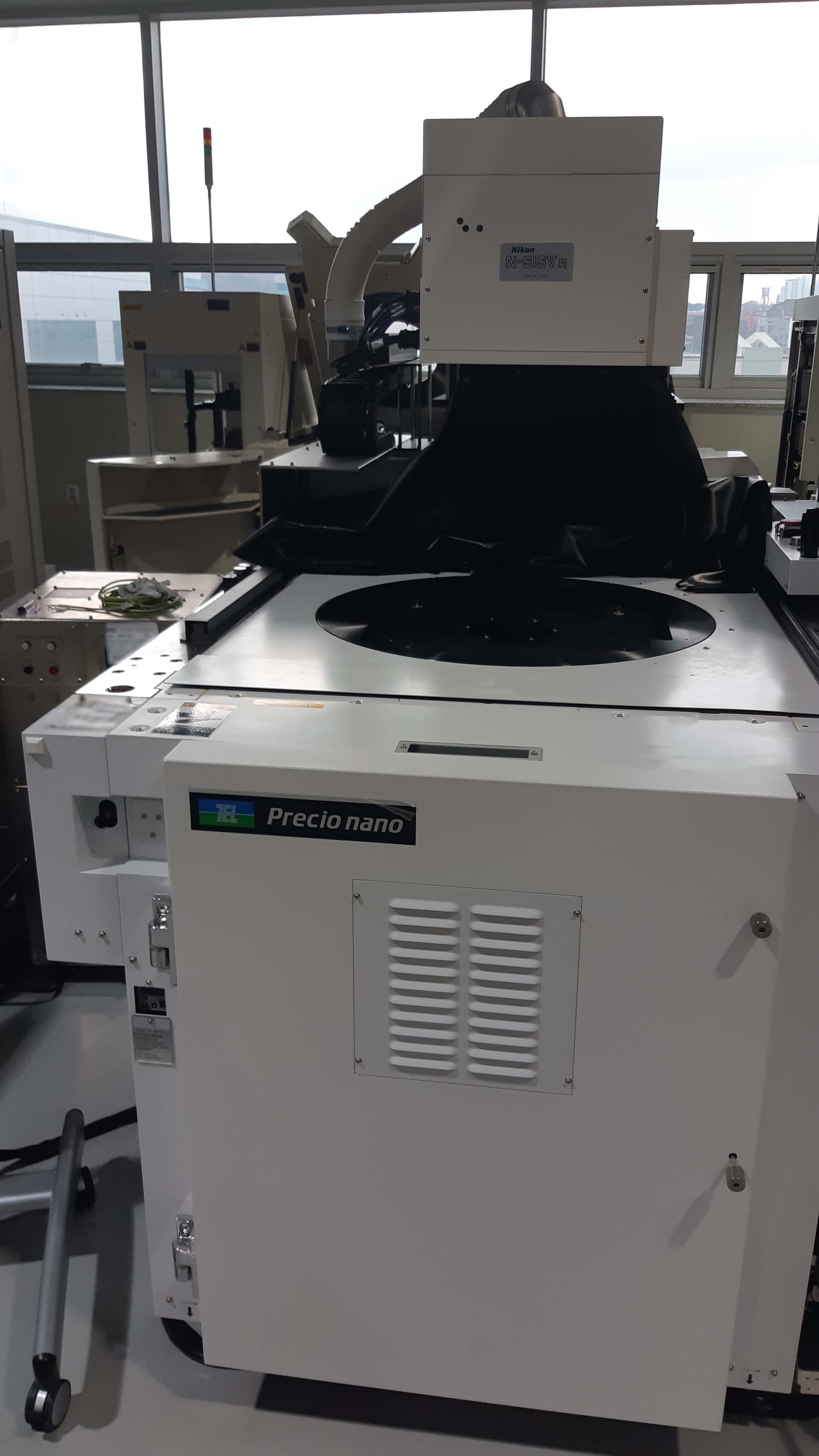
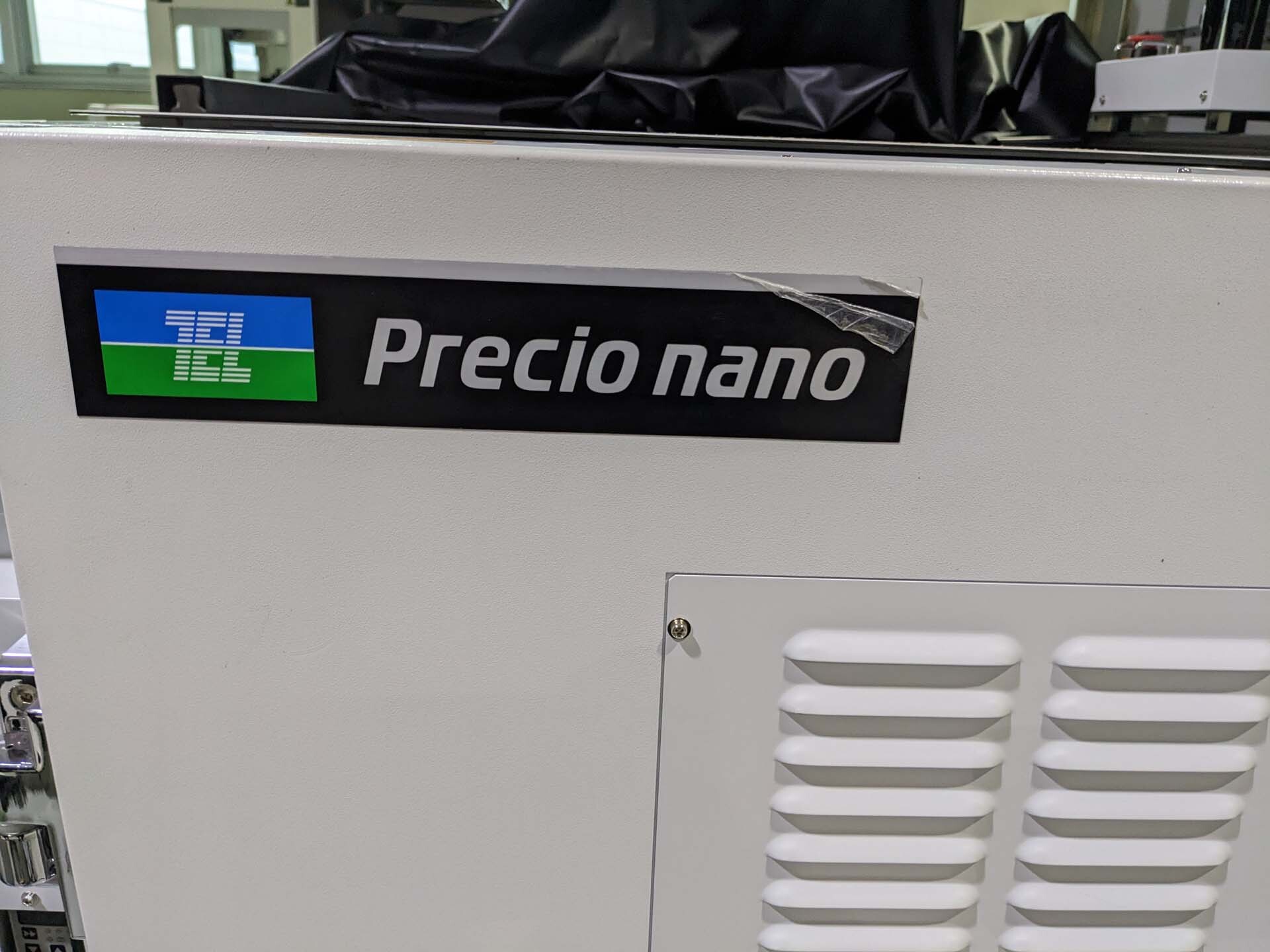
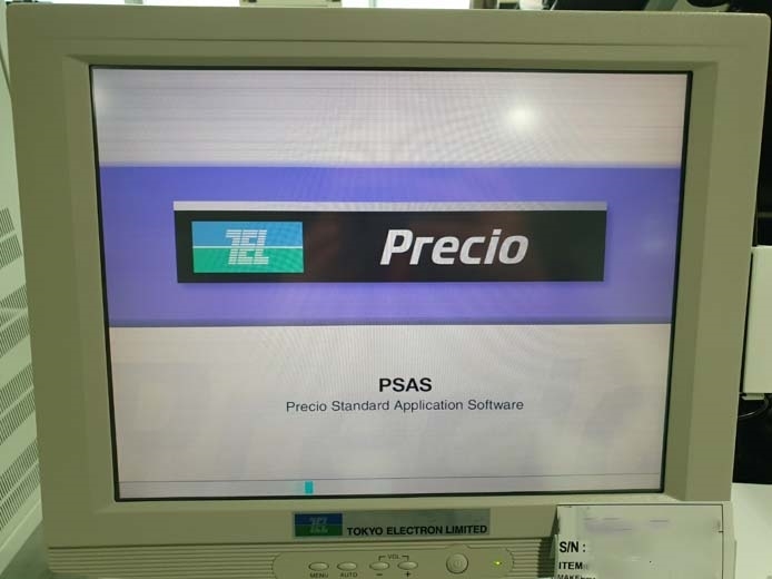
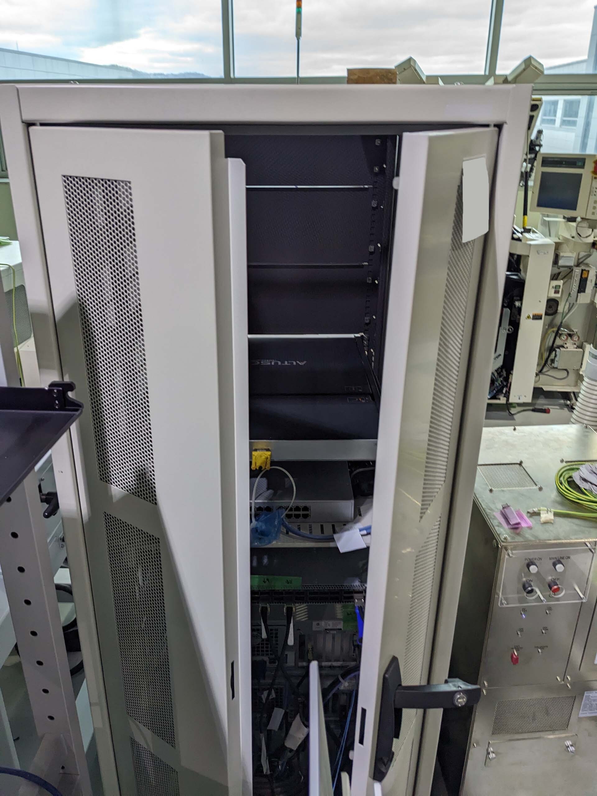
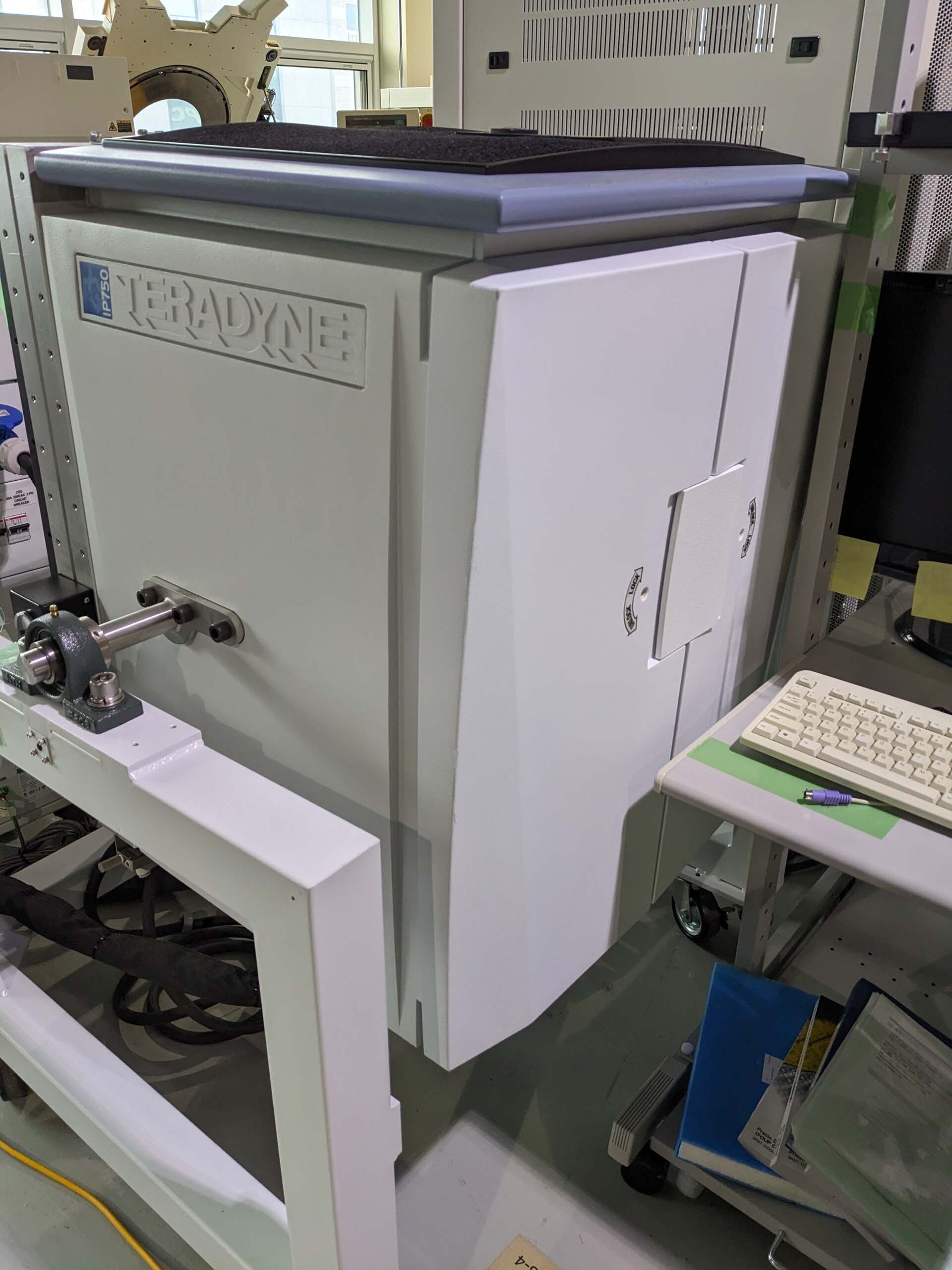
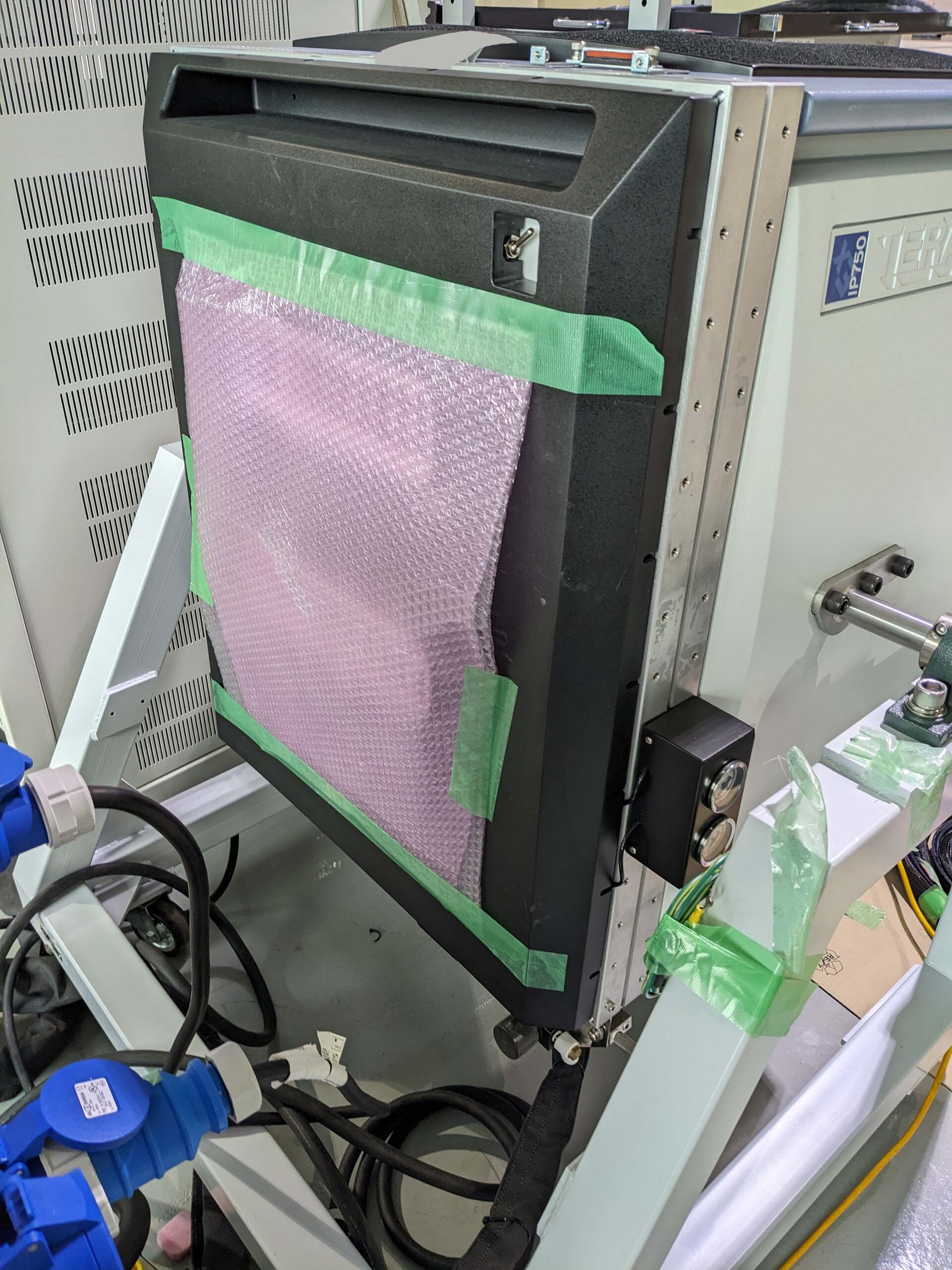
Used TEL / TOKYO ELECTRON Precio Nano #293663555 for sale
URL successfully copied!
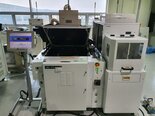
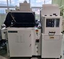
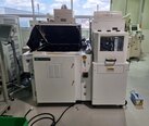
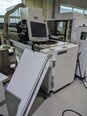
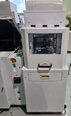
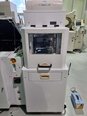
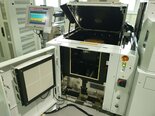
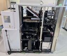
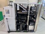
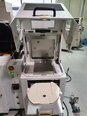
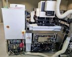
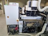
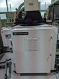
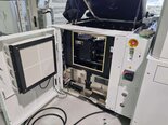
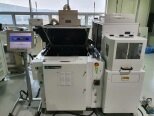
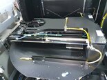
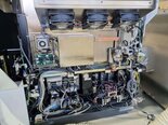
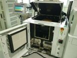
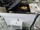
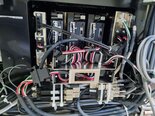
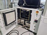
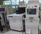
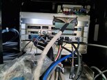
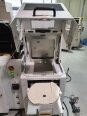
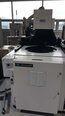
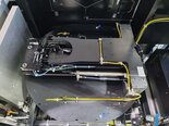
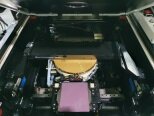

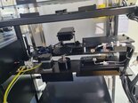
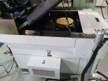
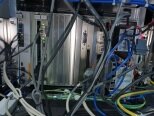
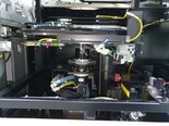
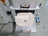
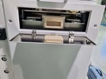
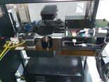
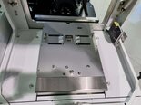
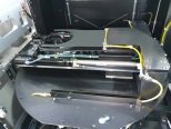
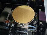
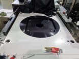
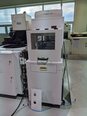
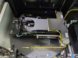
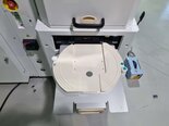
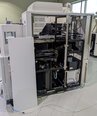
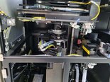
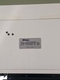
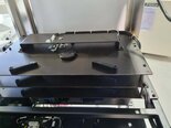
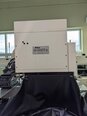
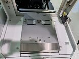
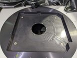
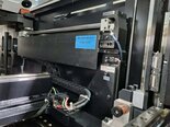
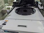
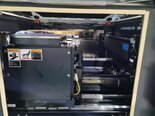
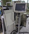
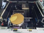
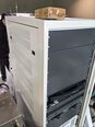
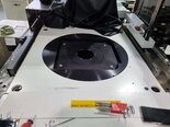
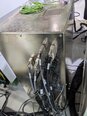
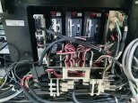
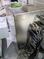
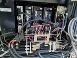

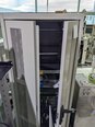
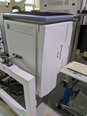
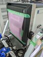
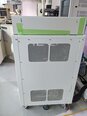
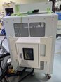
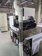
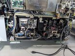
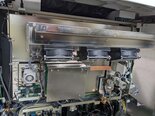
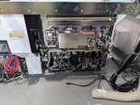
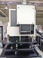
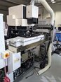
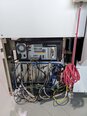
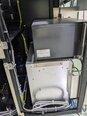
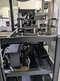
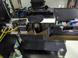
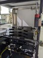
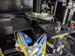
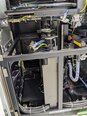

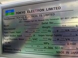
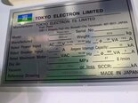
Tap to zoom
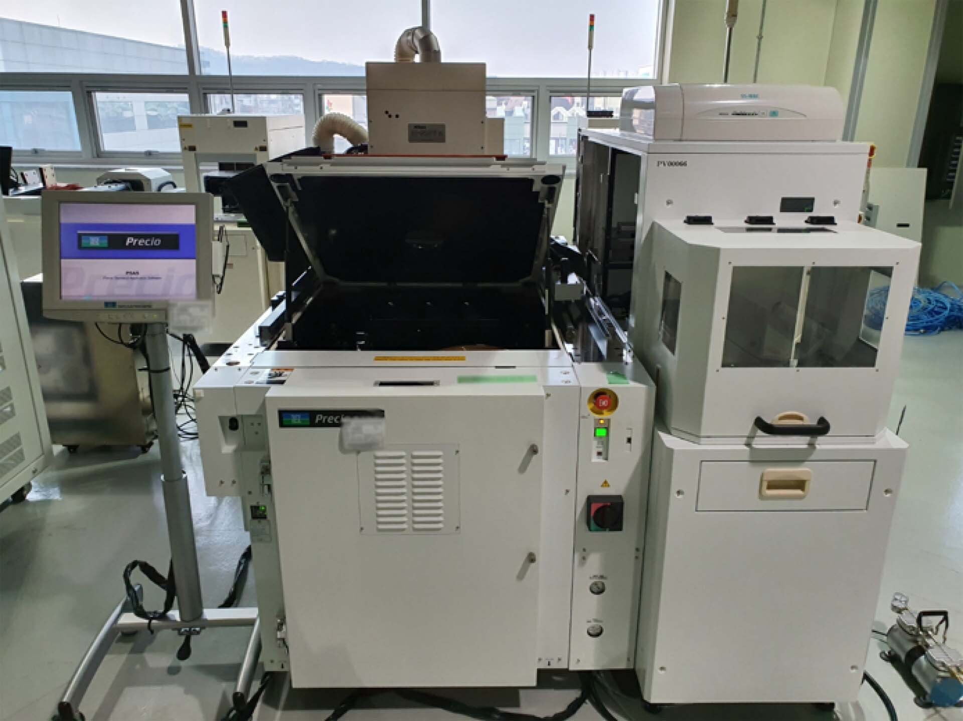

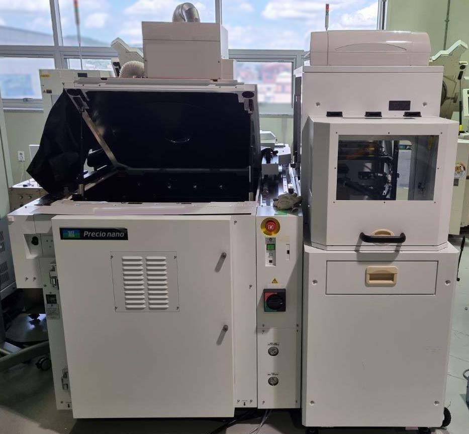
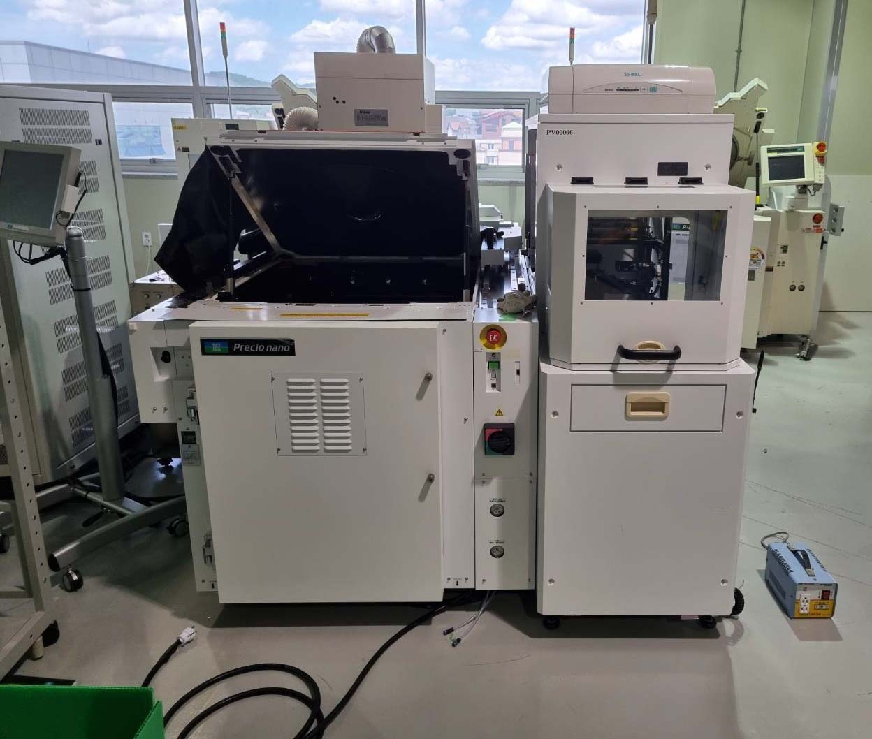
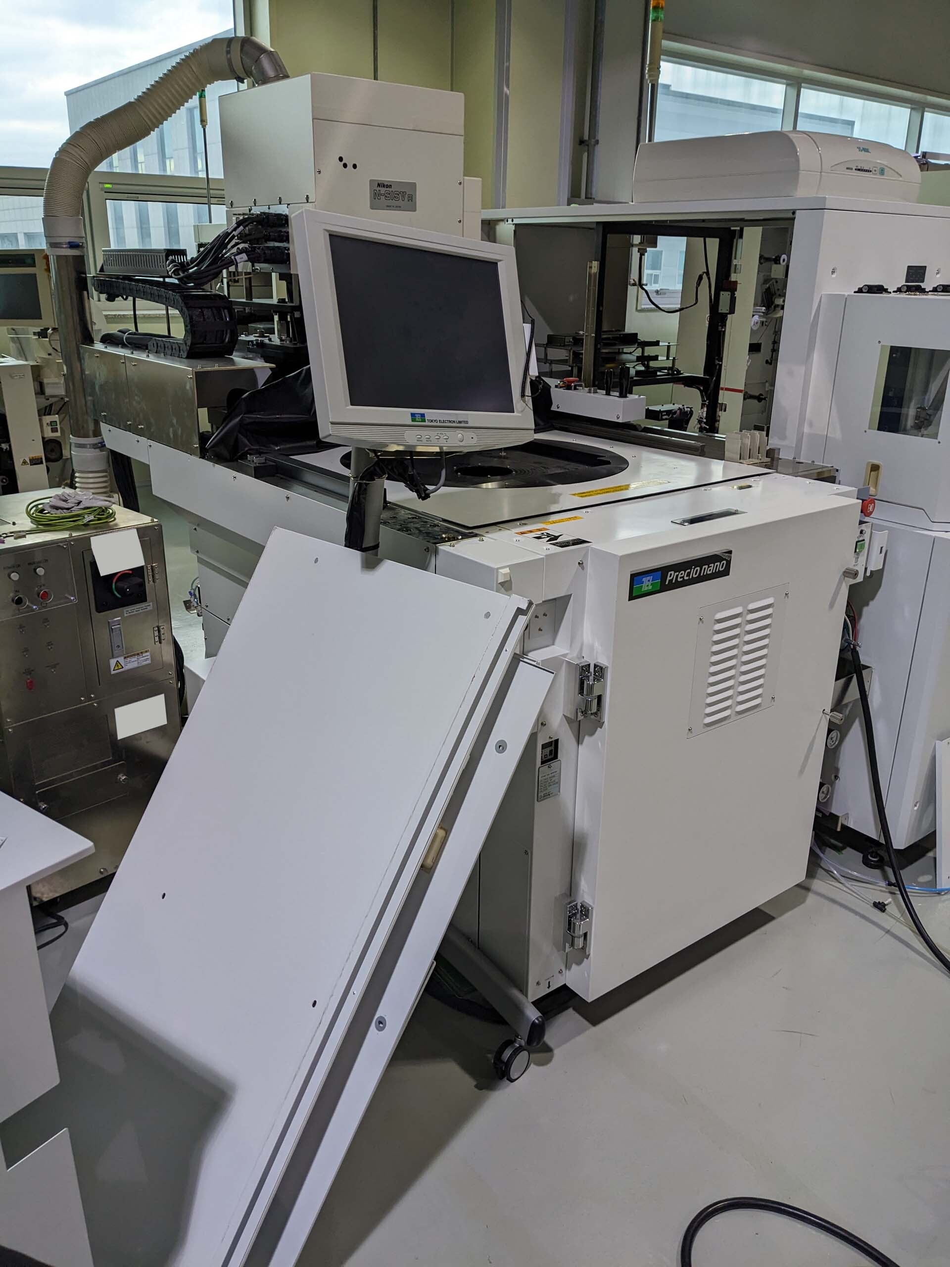
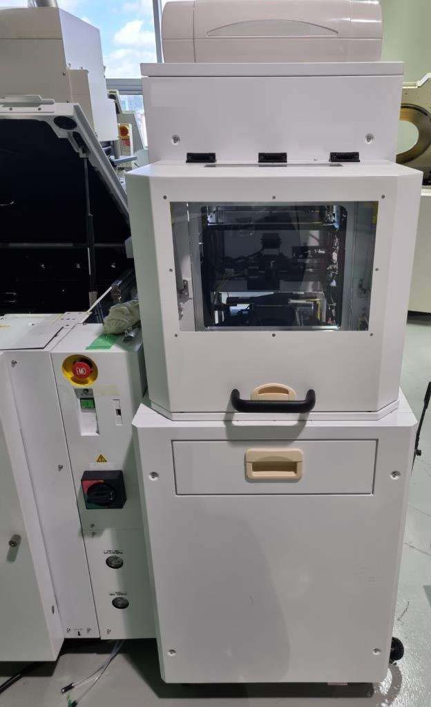
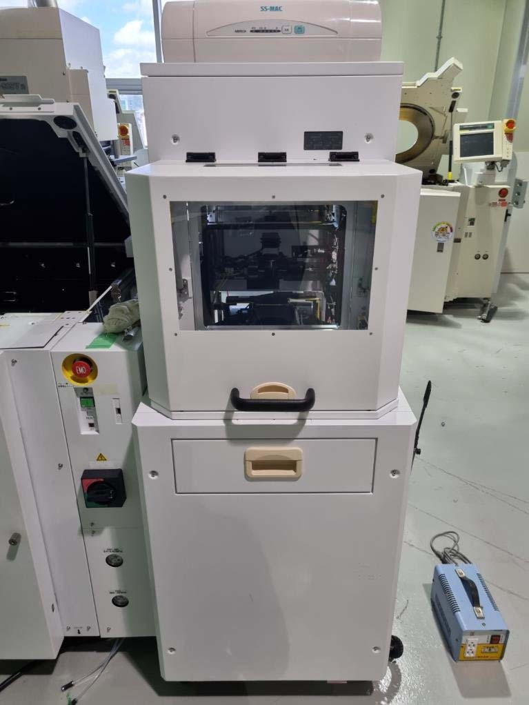
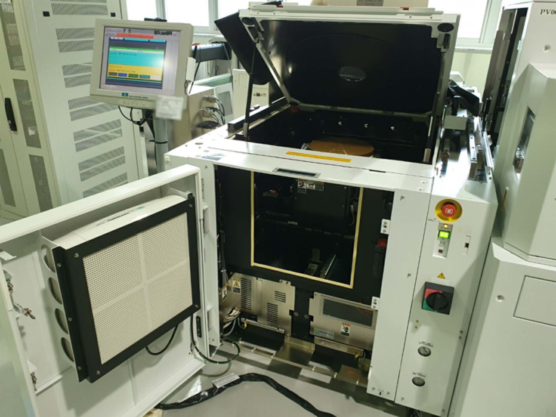
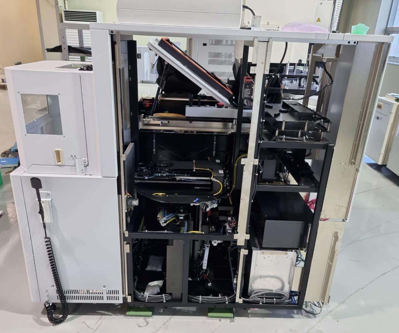
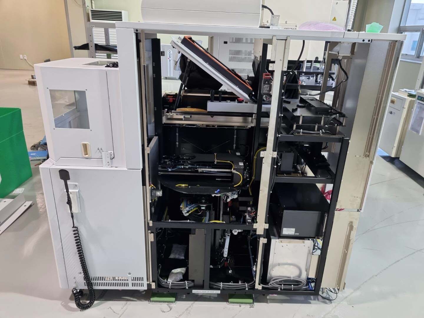
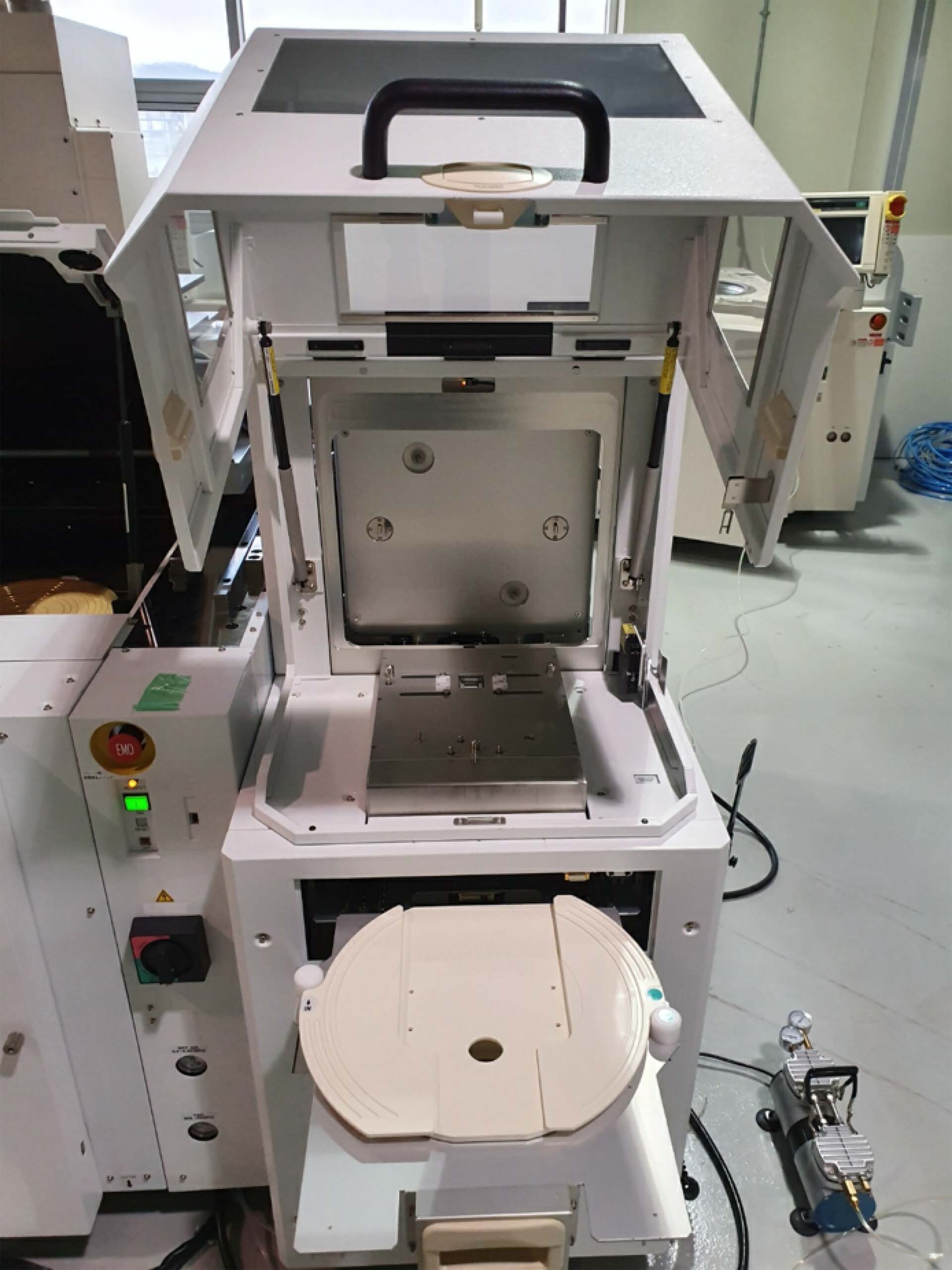
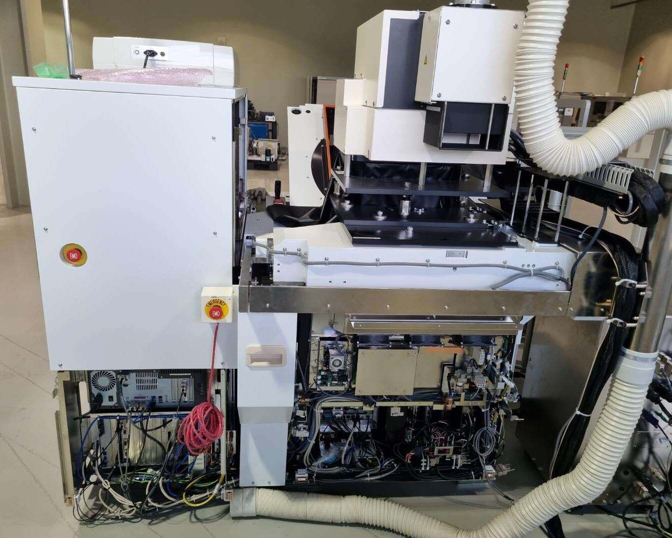
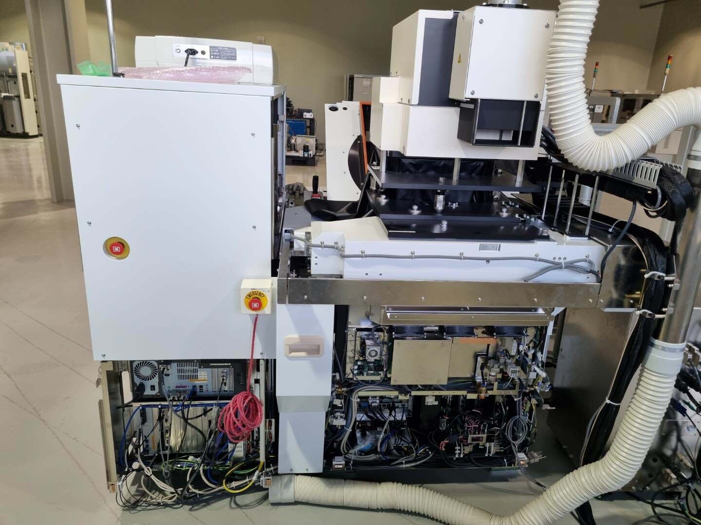
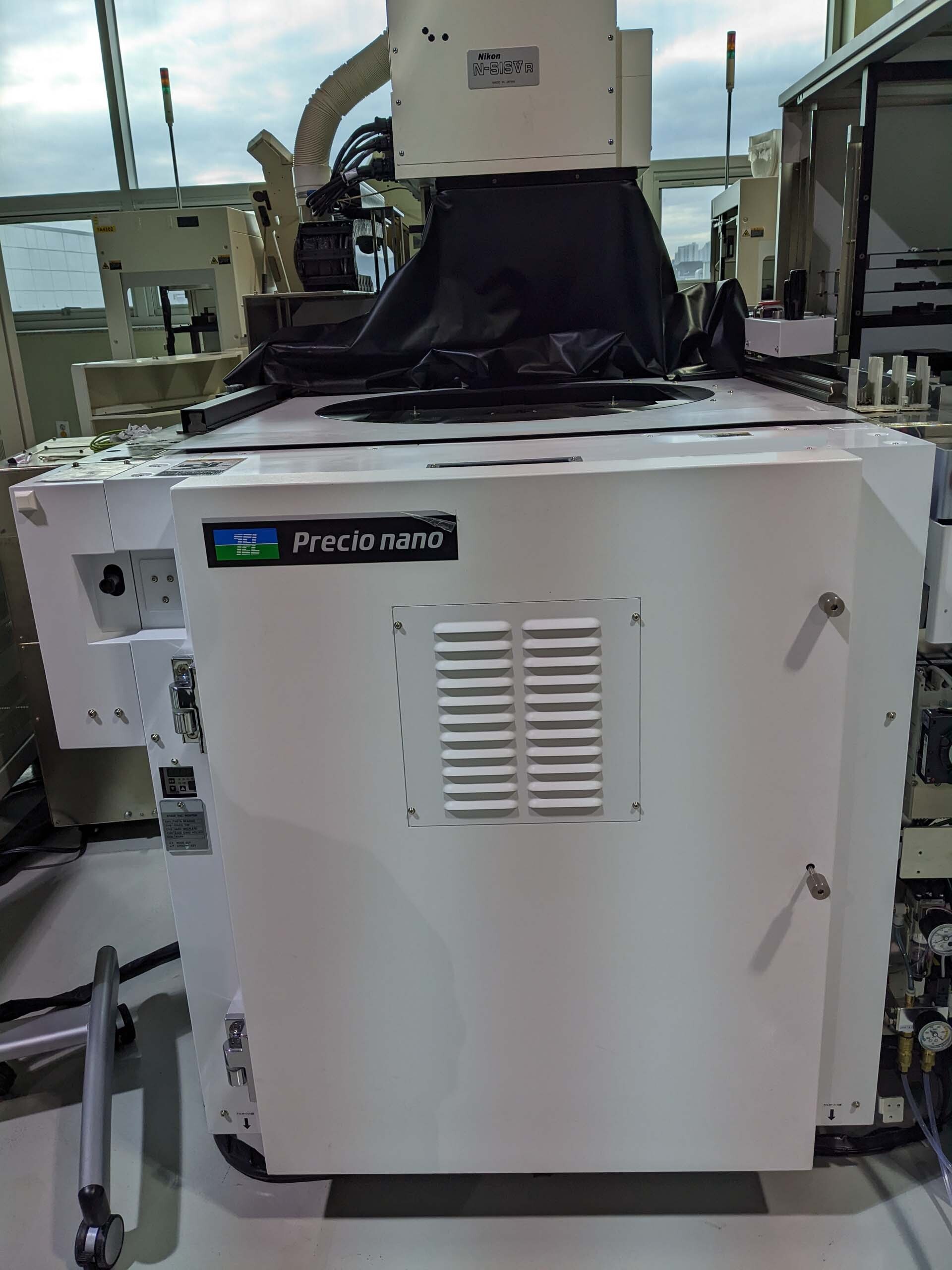
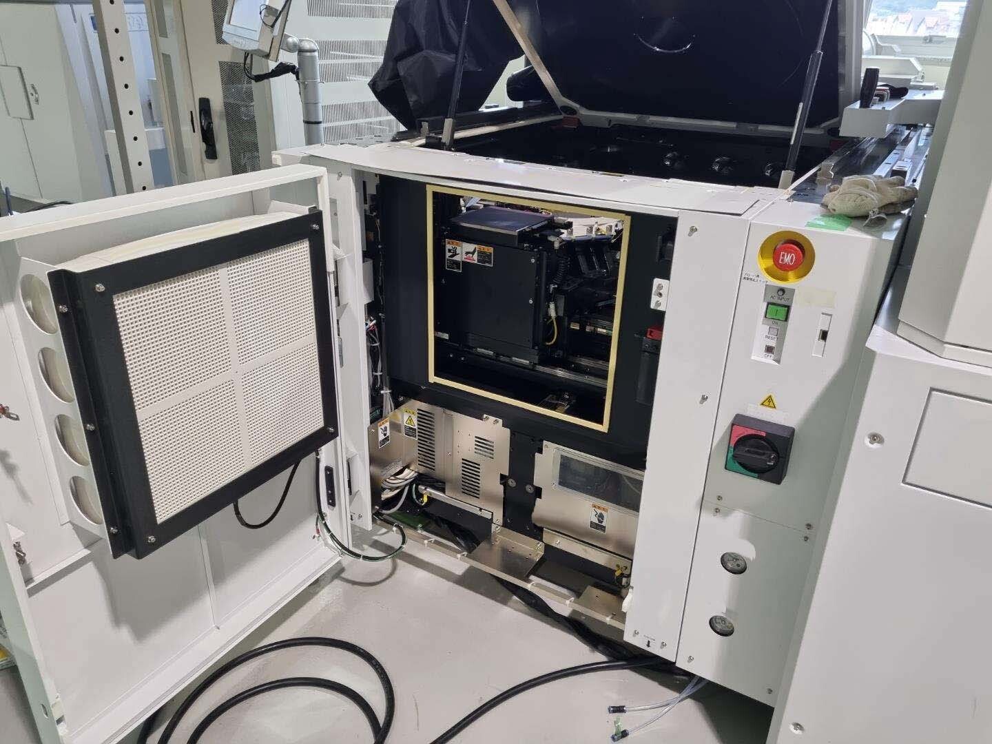
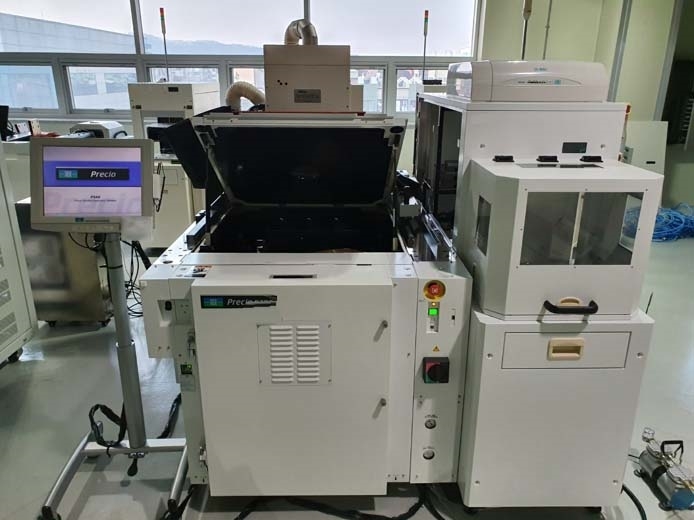
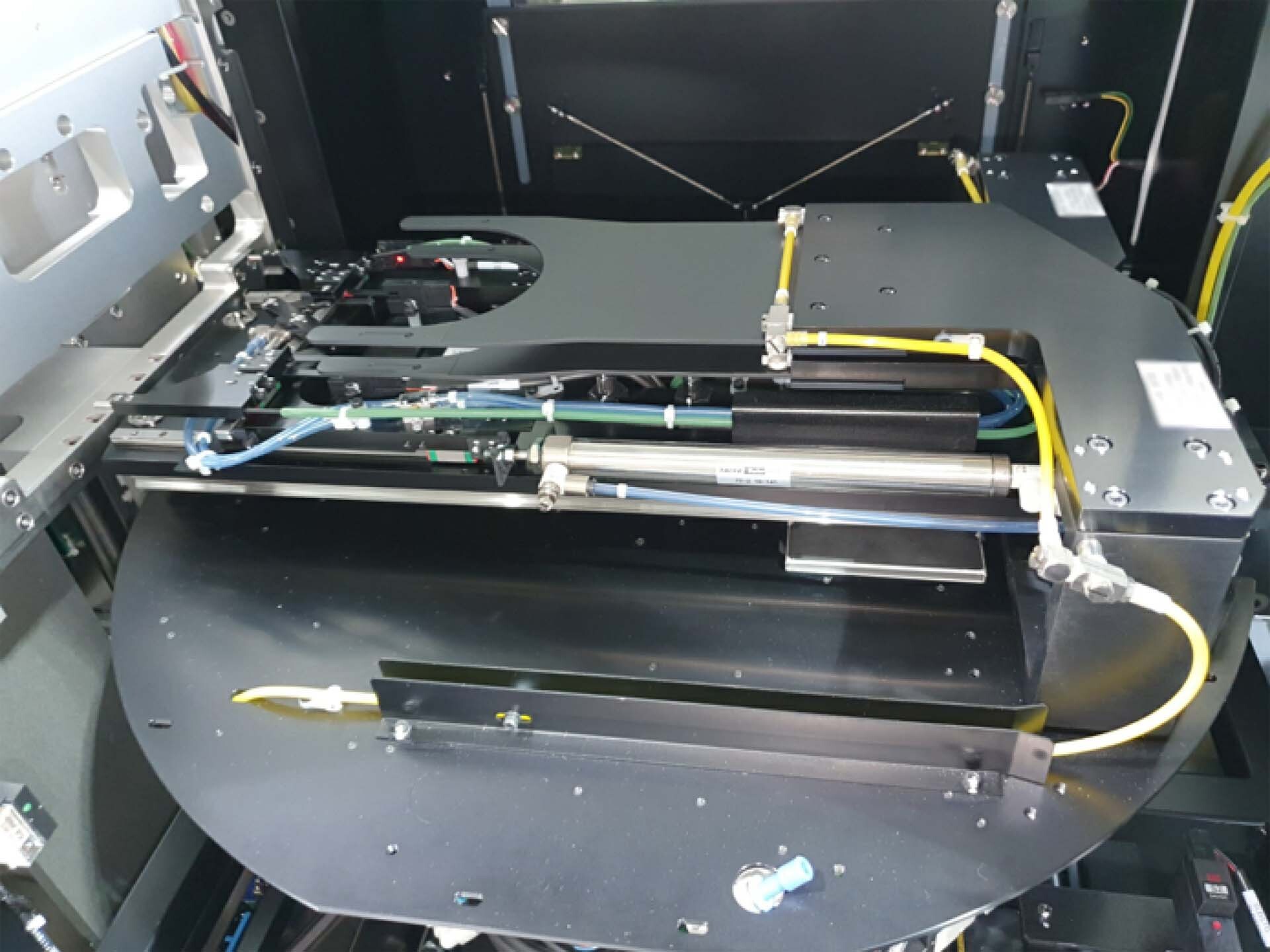
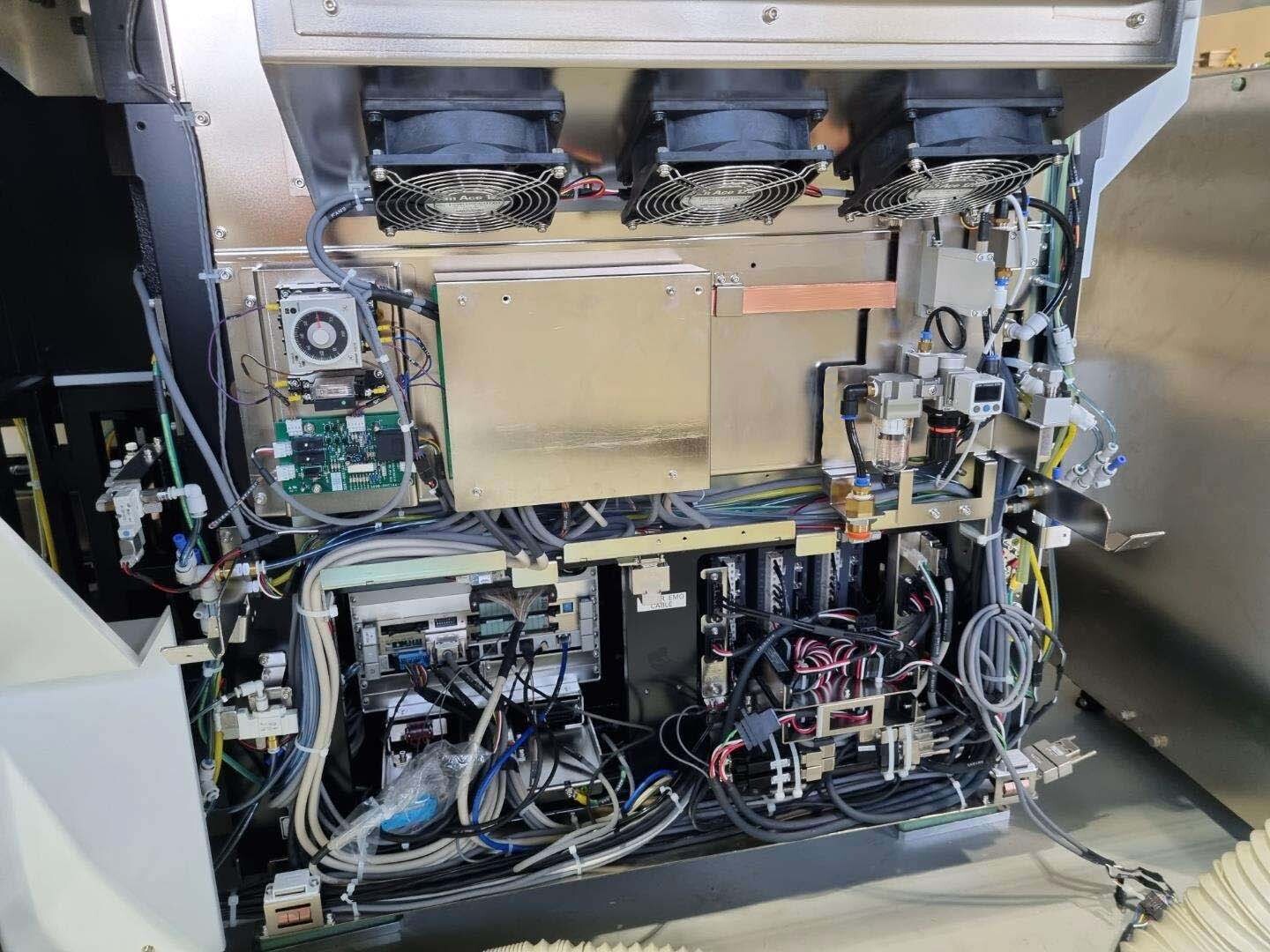
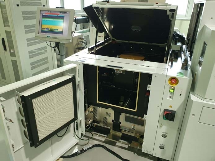
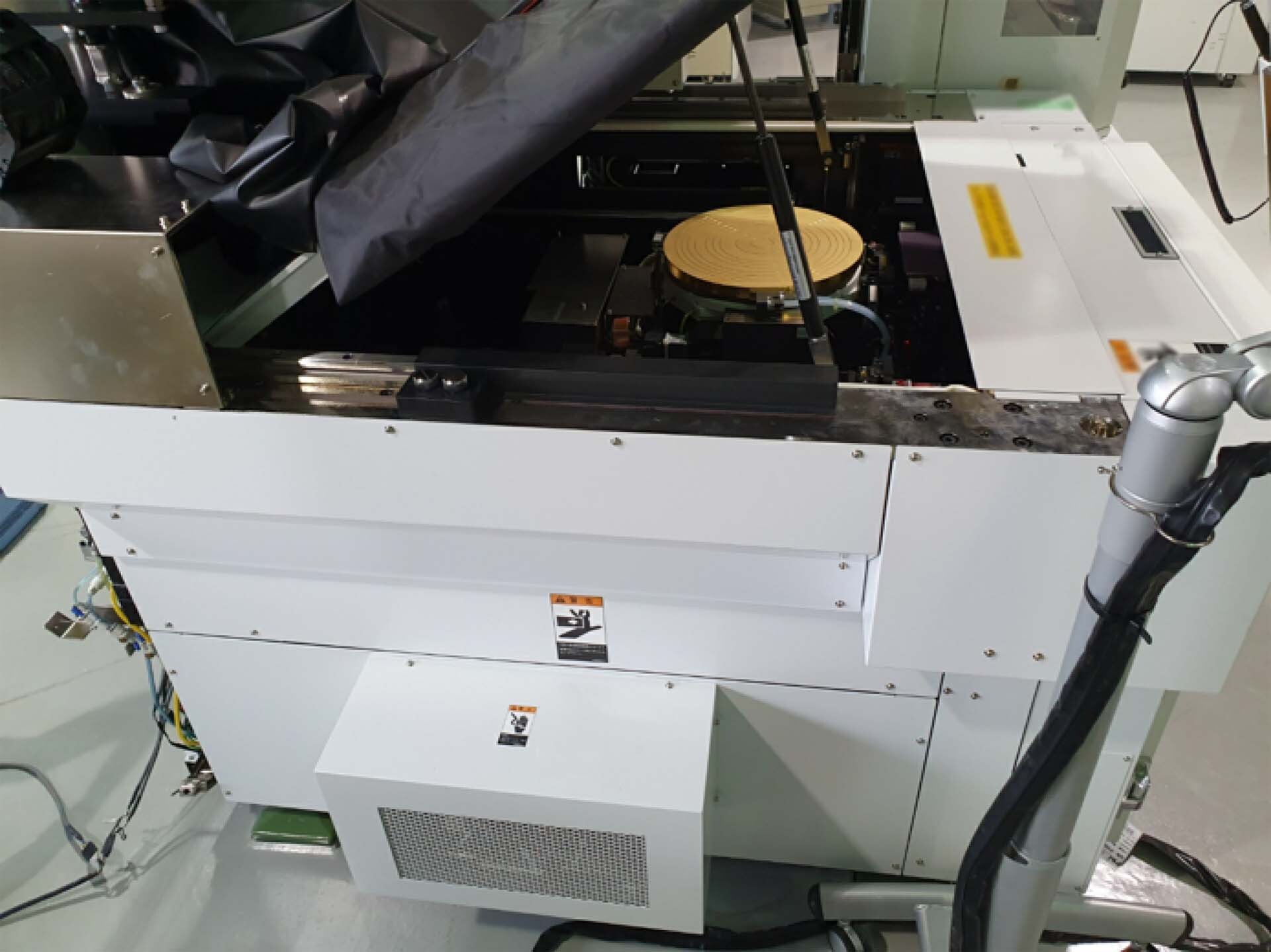
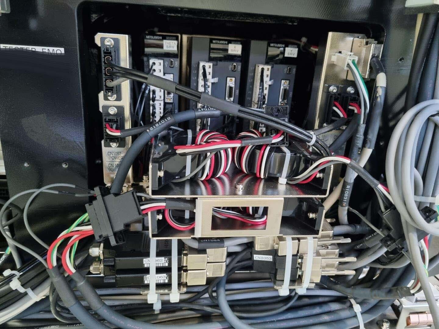
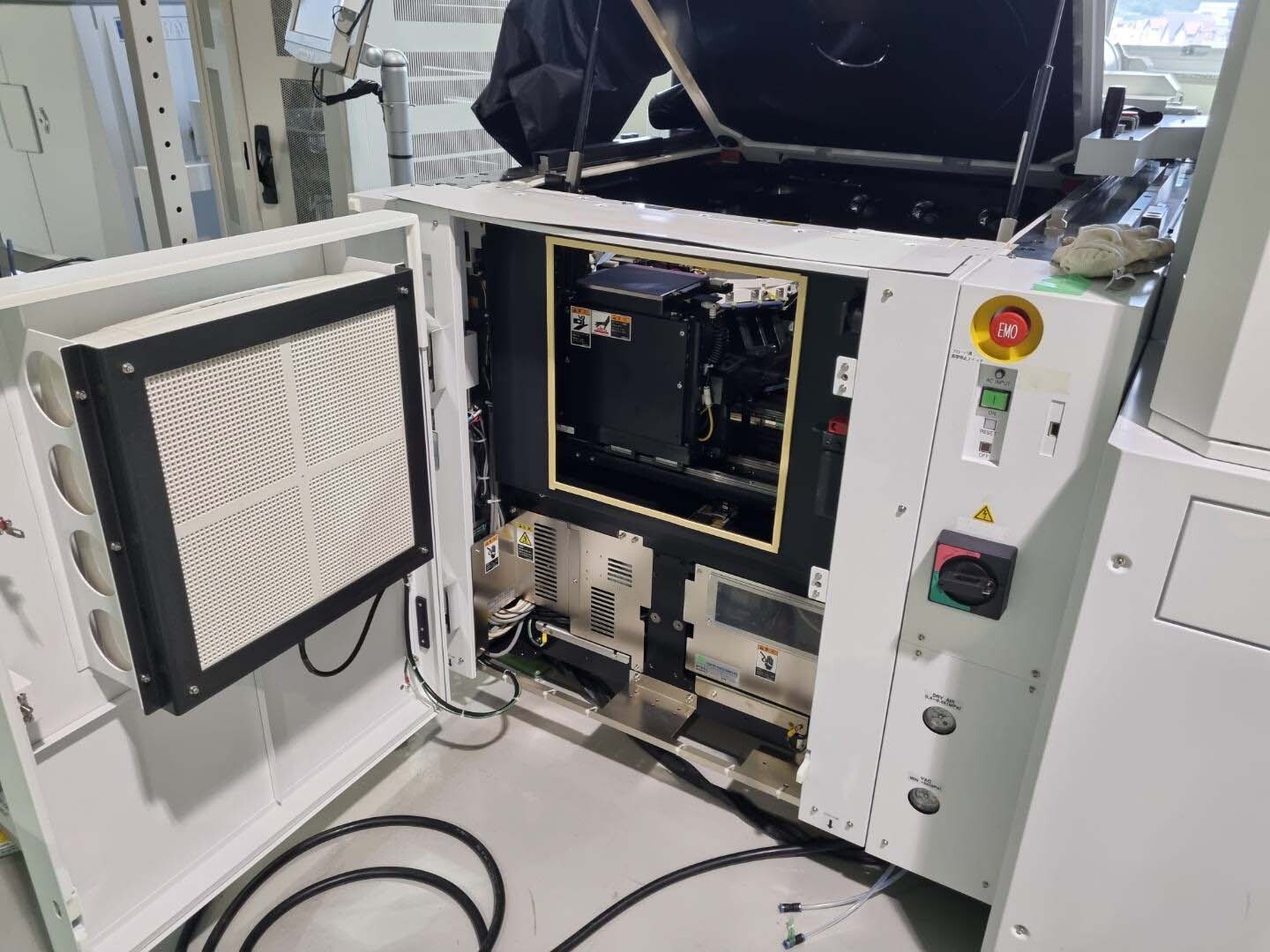
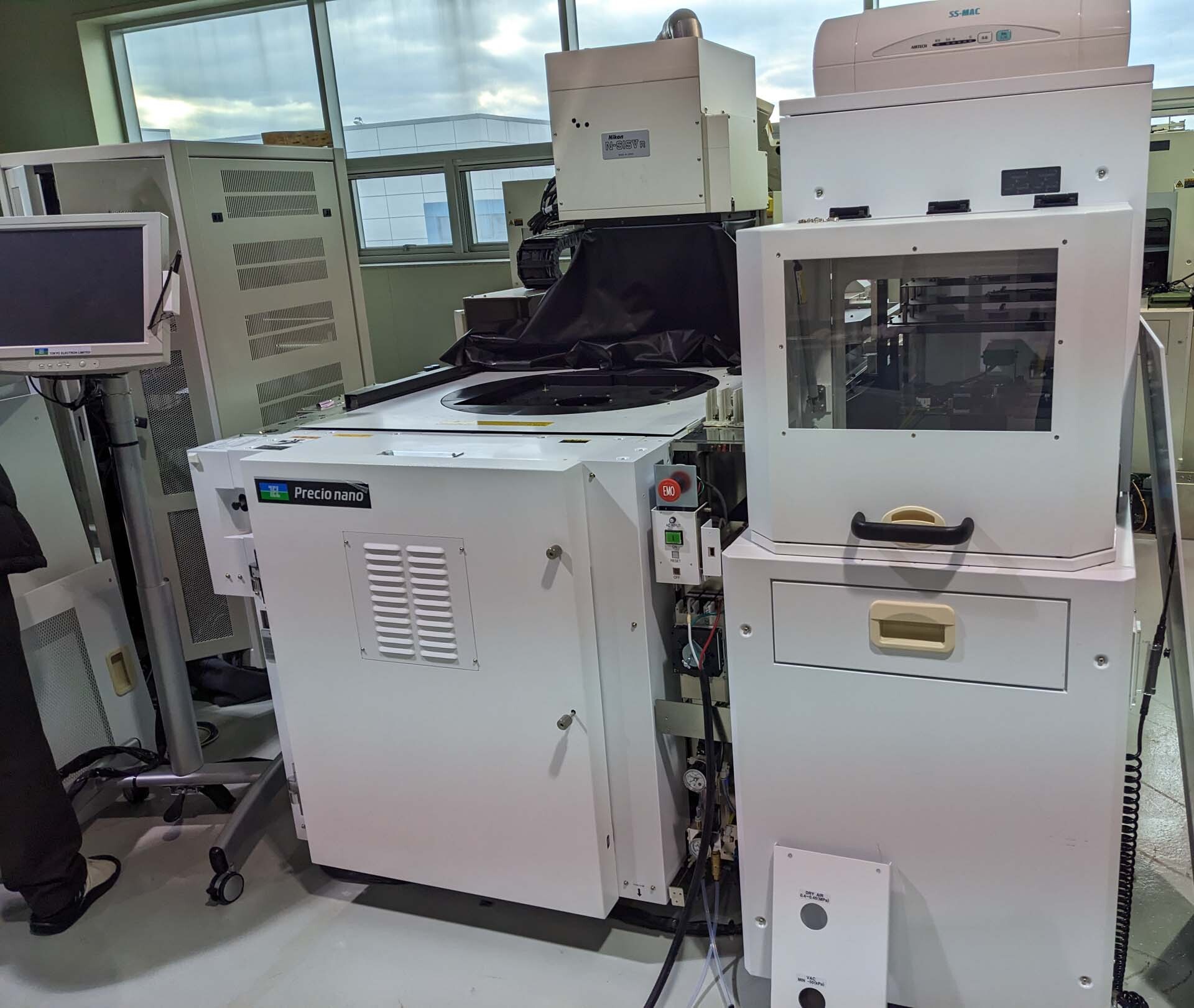
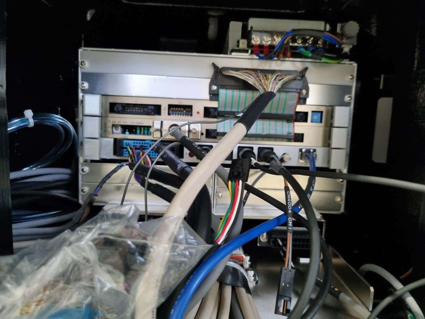
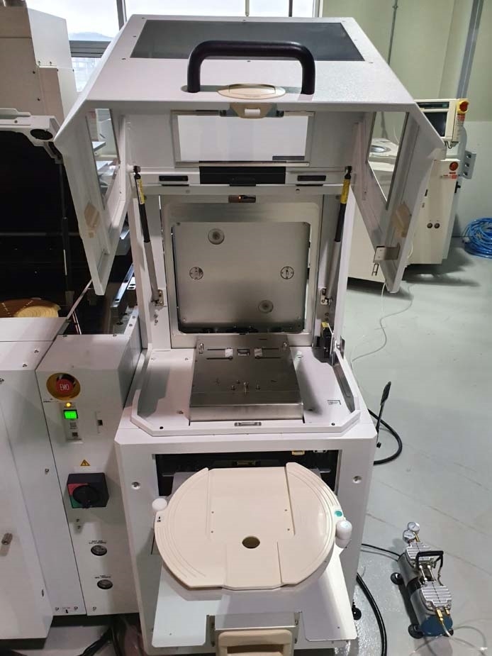
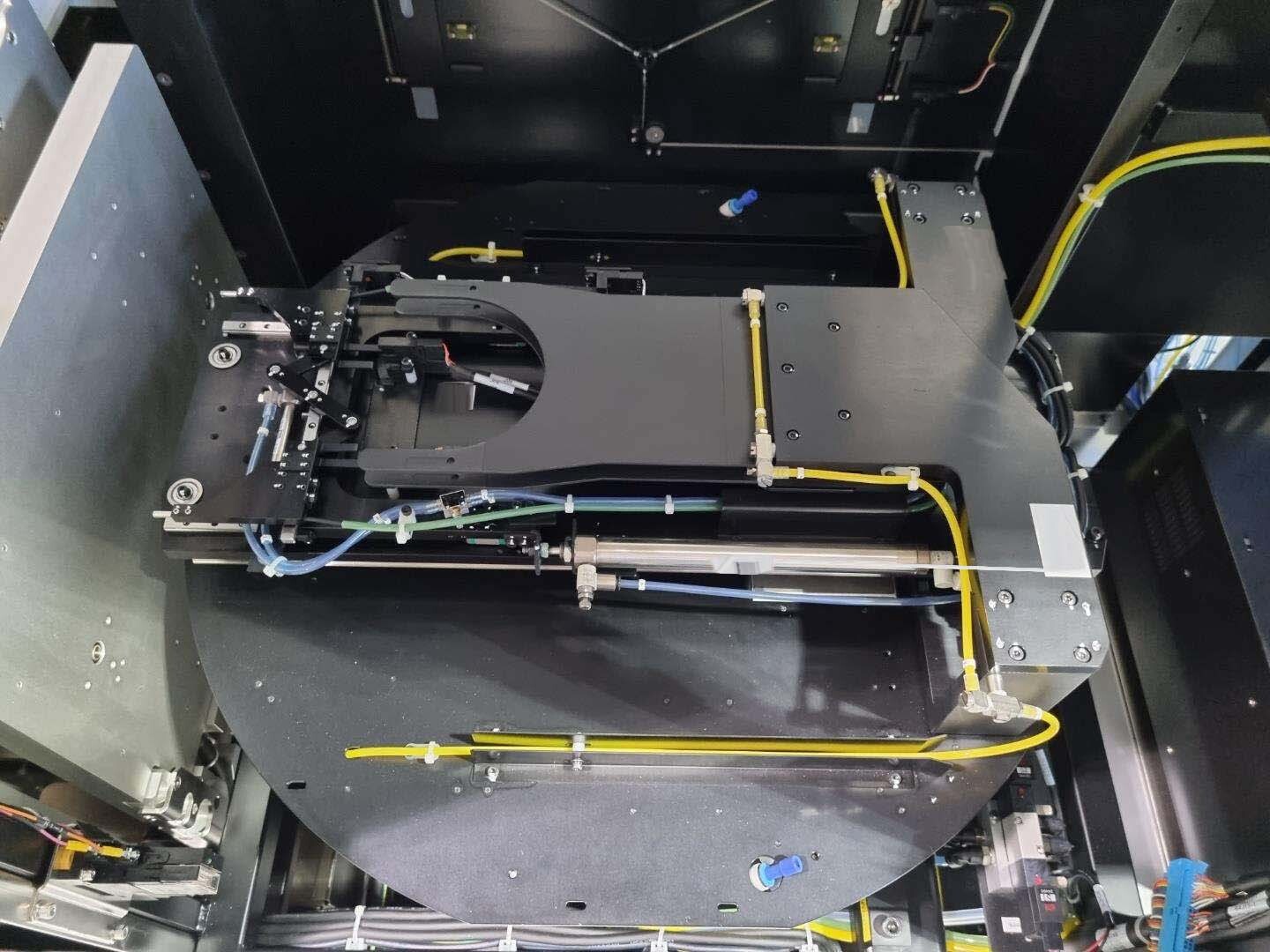
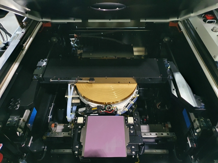
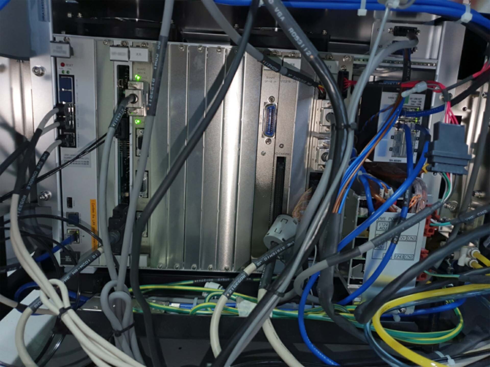
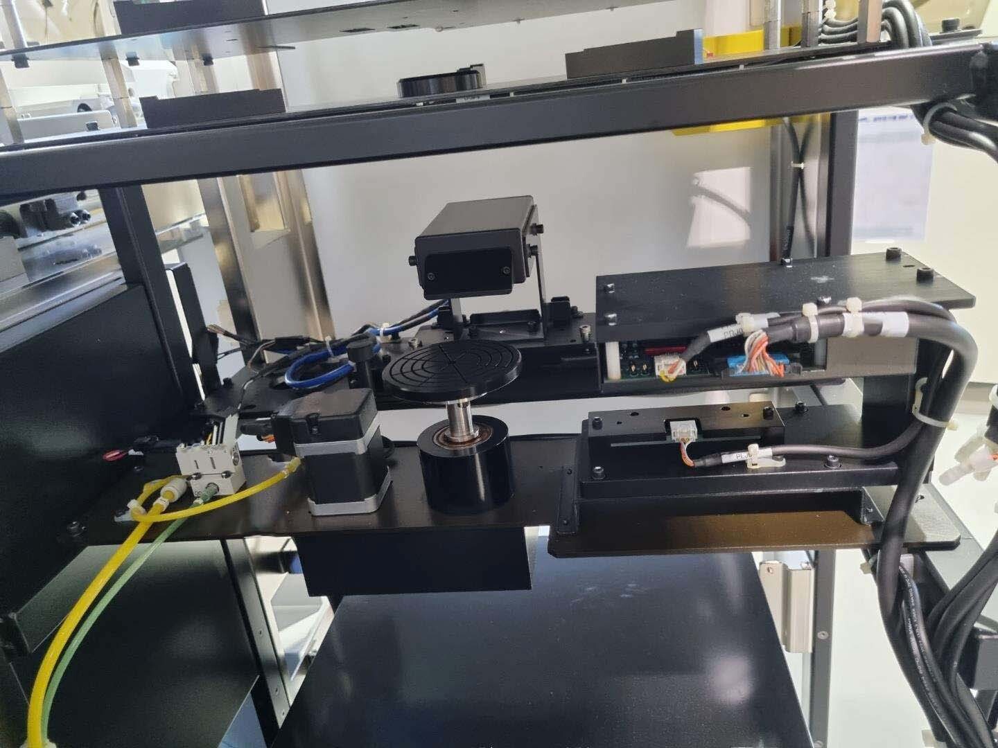
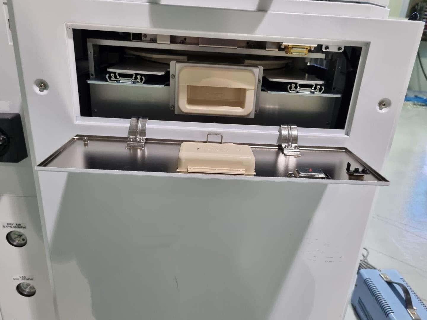
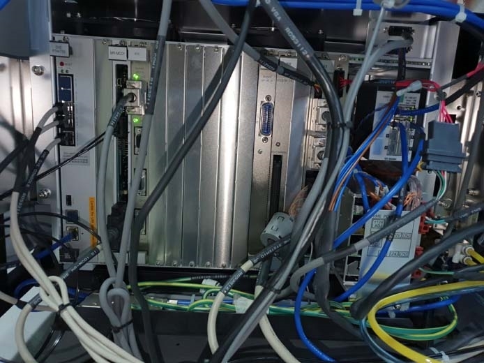
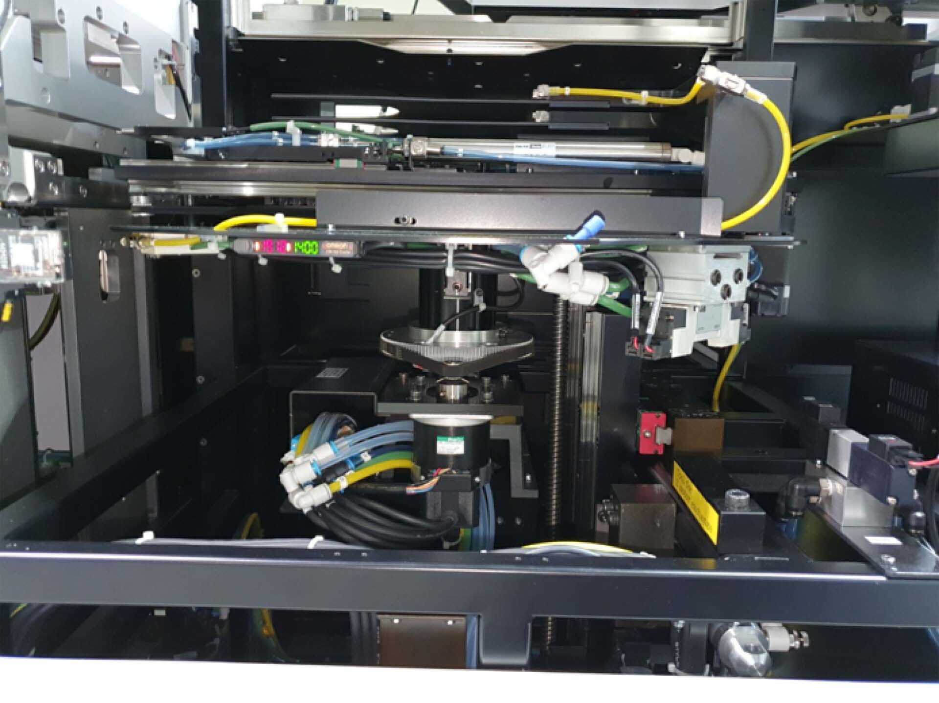
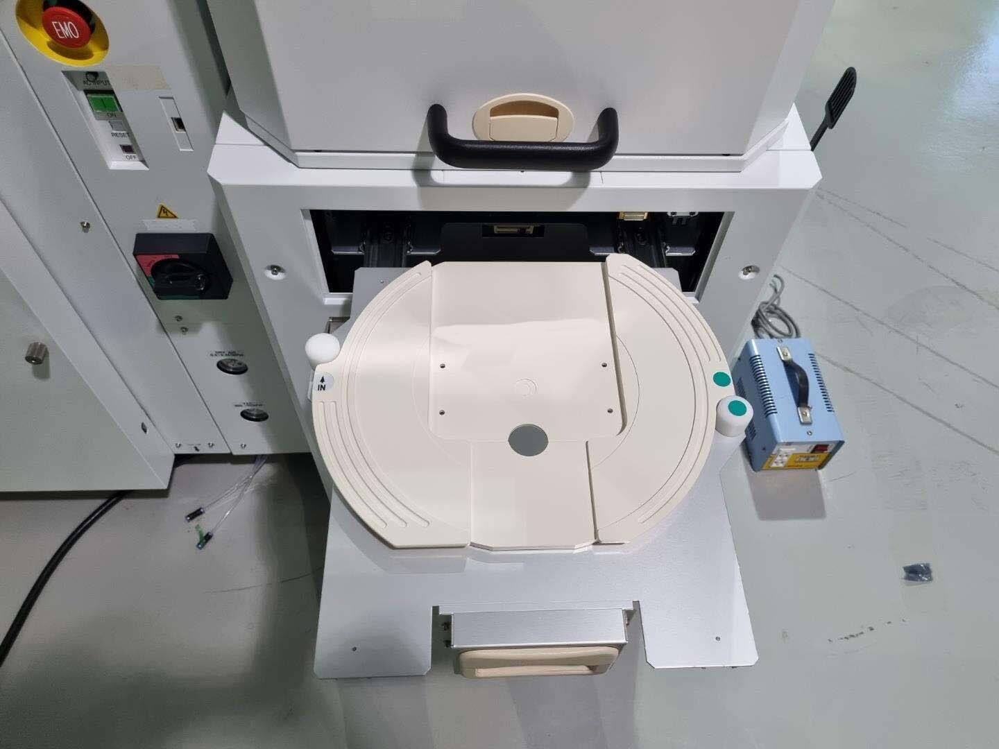
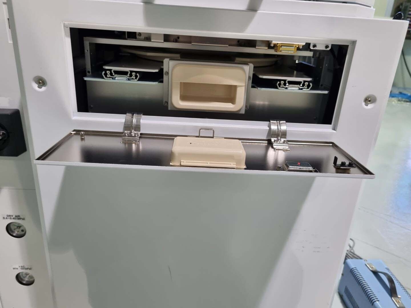
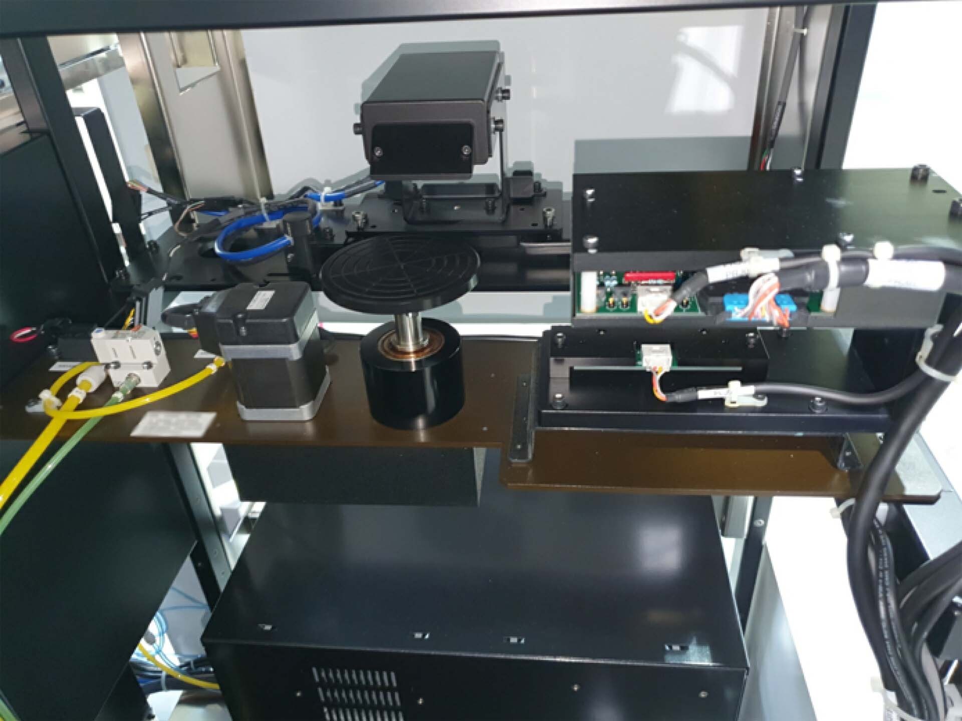
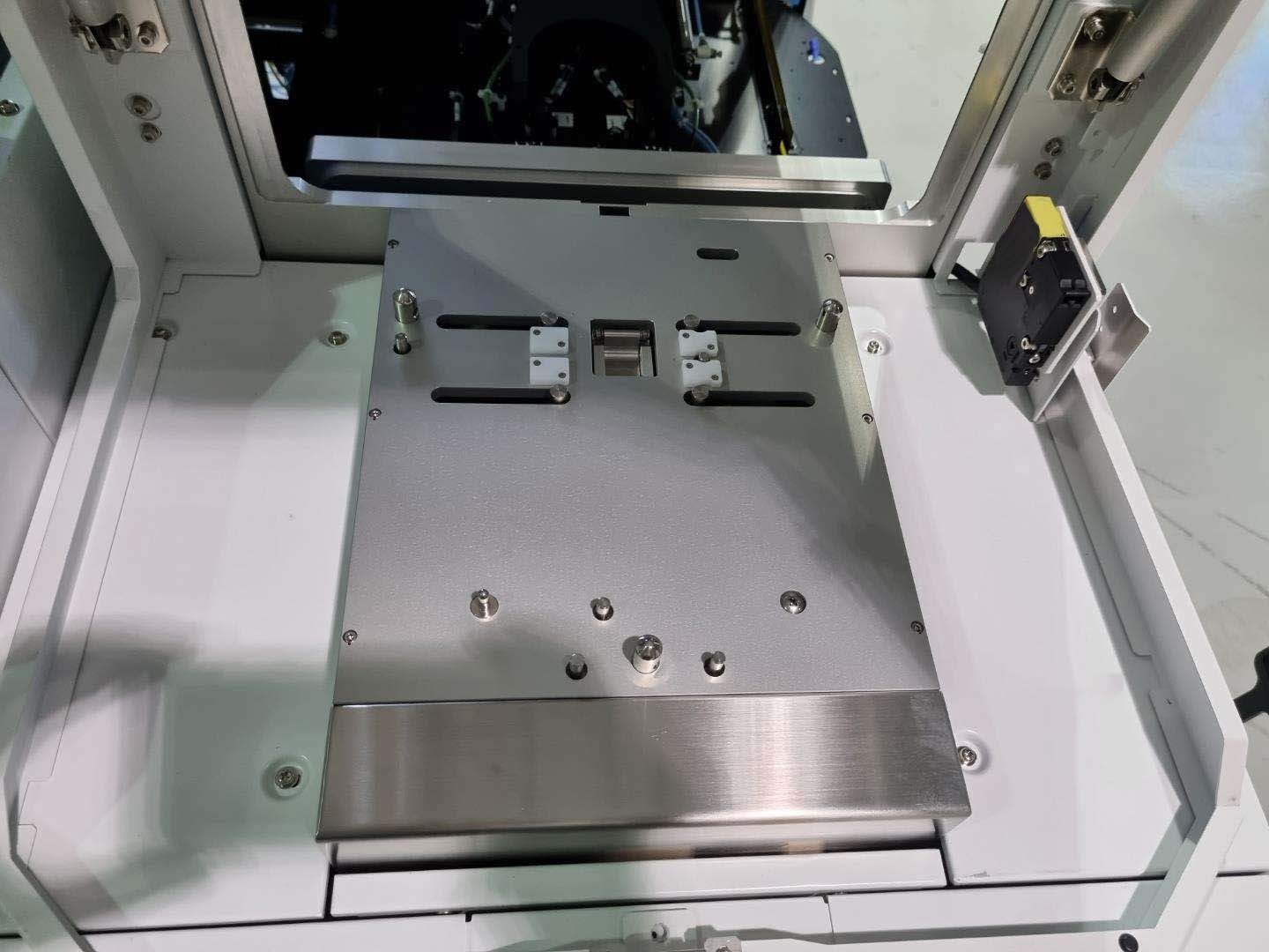
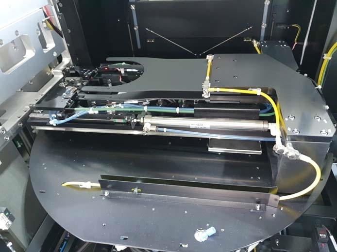
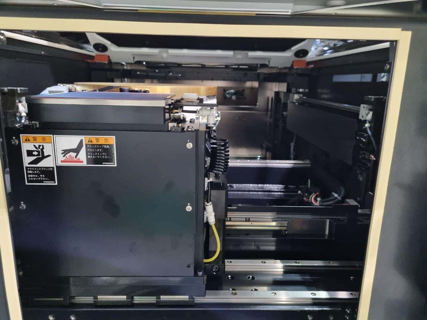
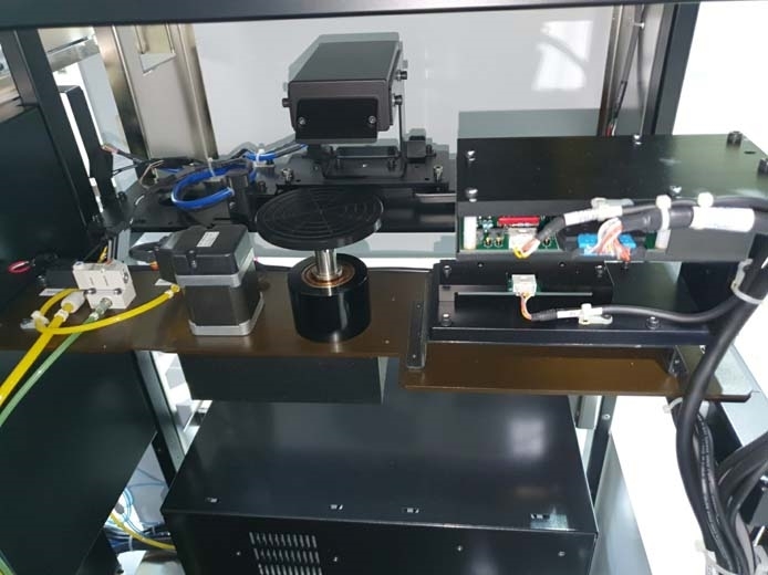
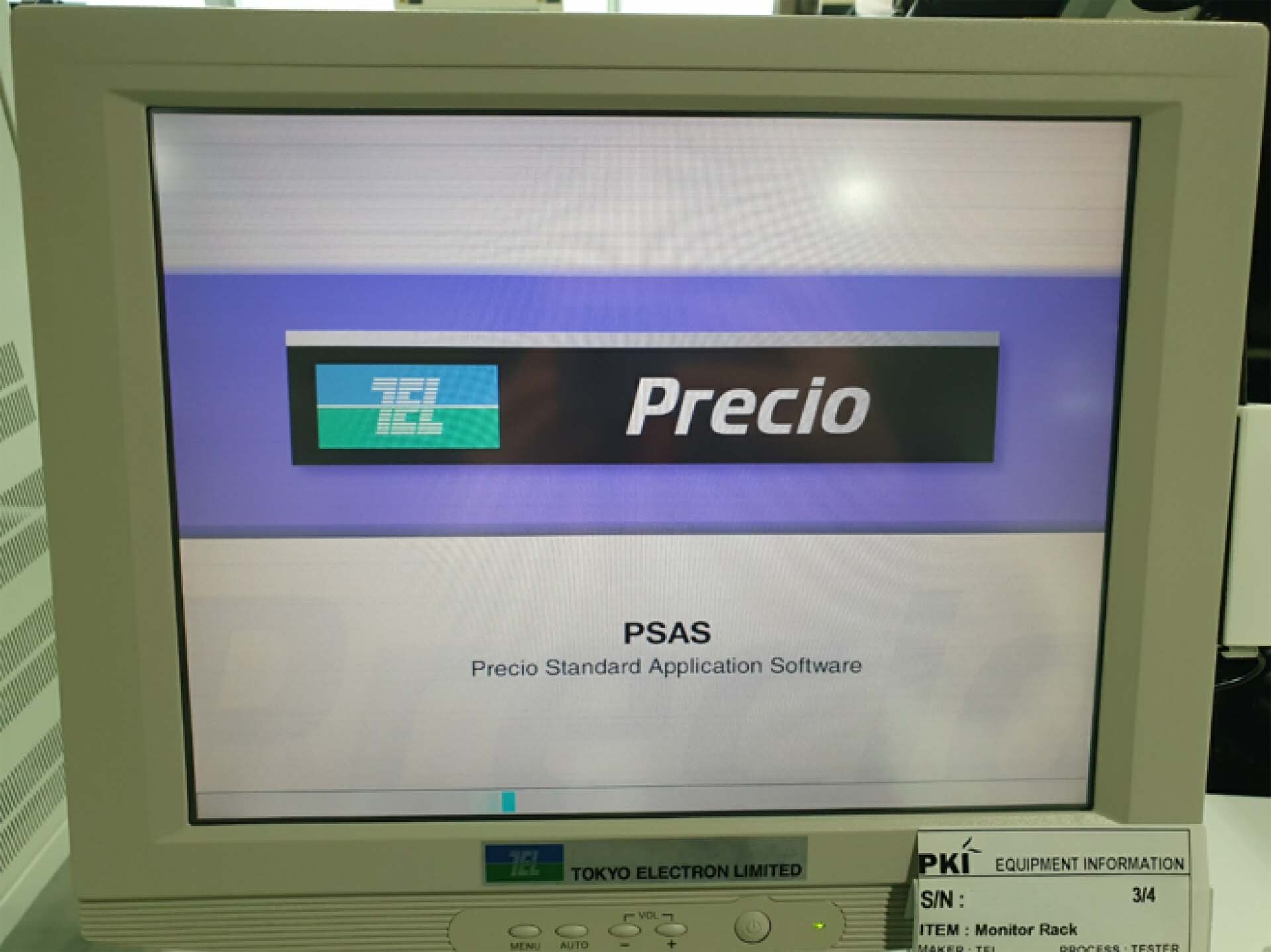
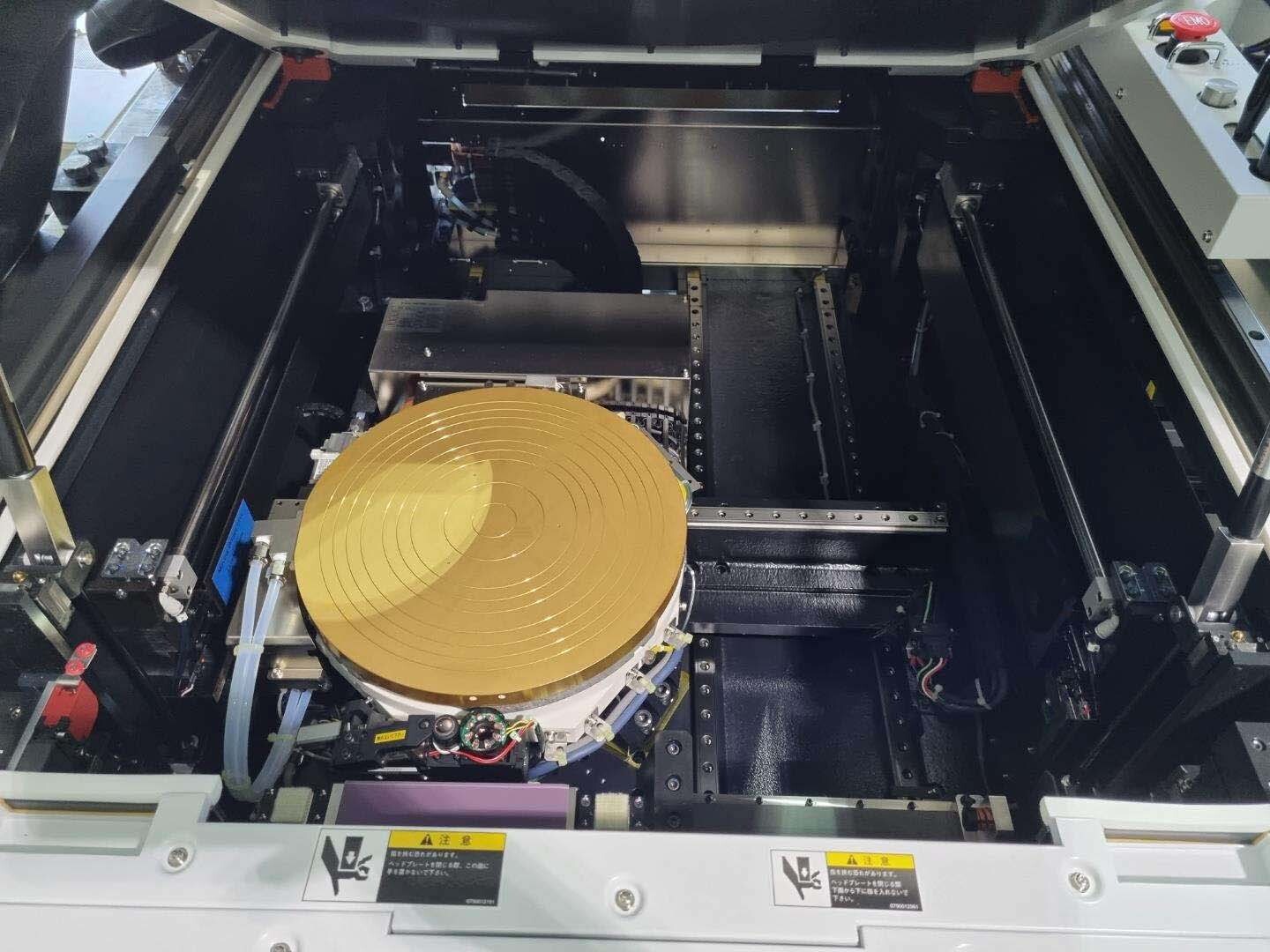
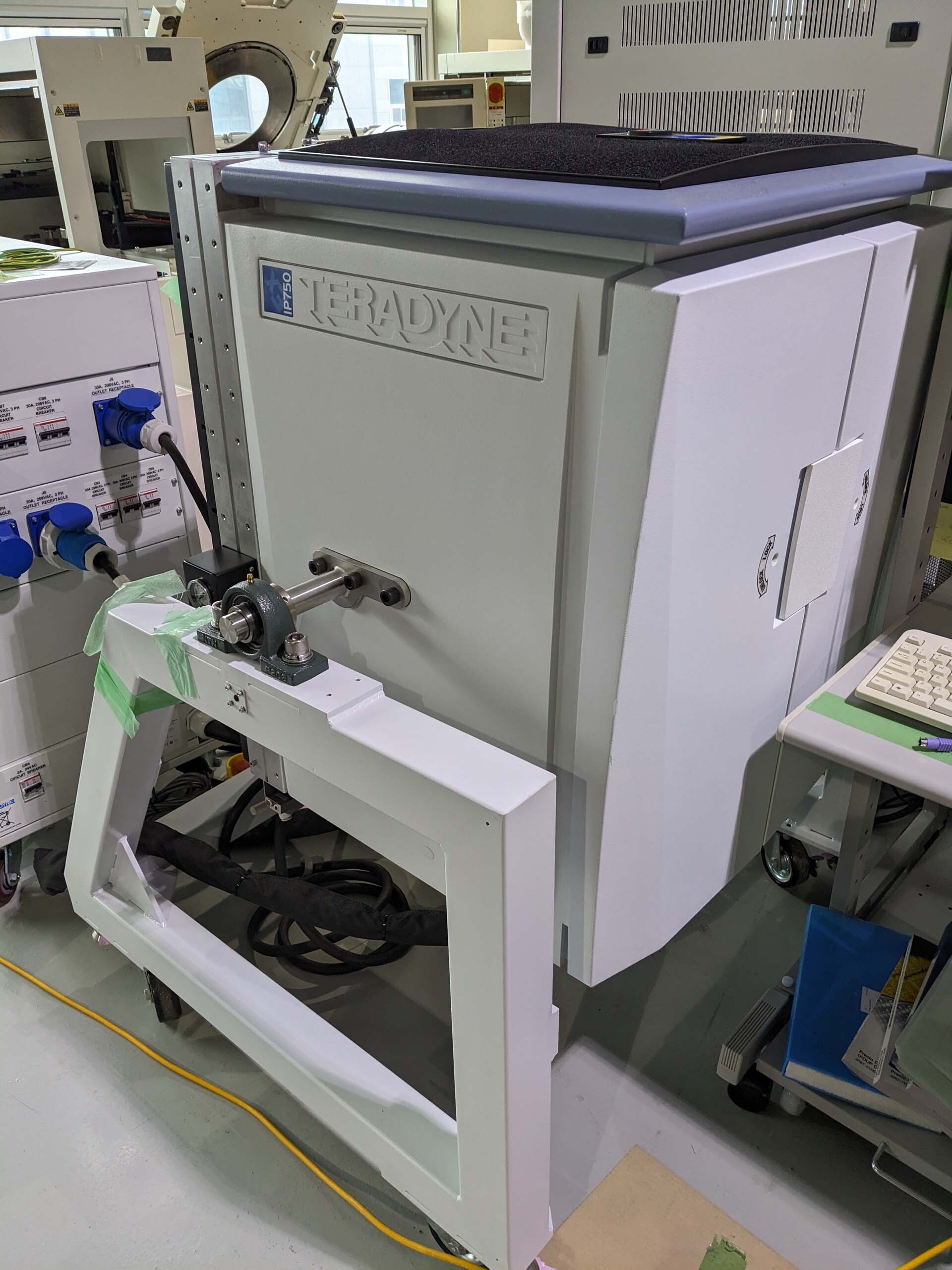
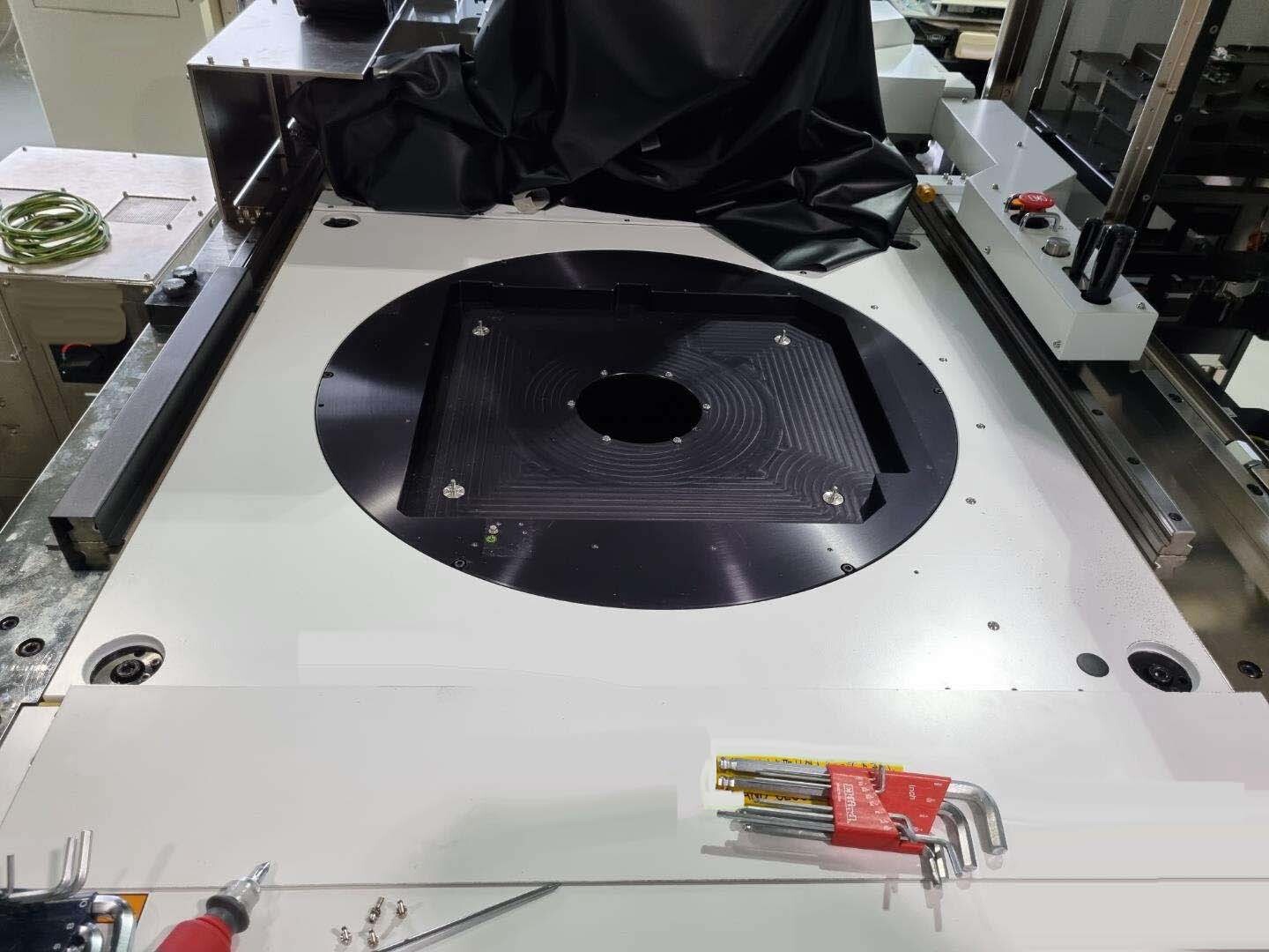
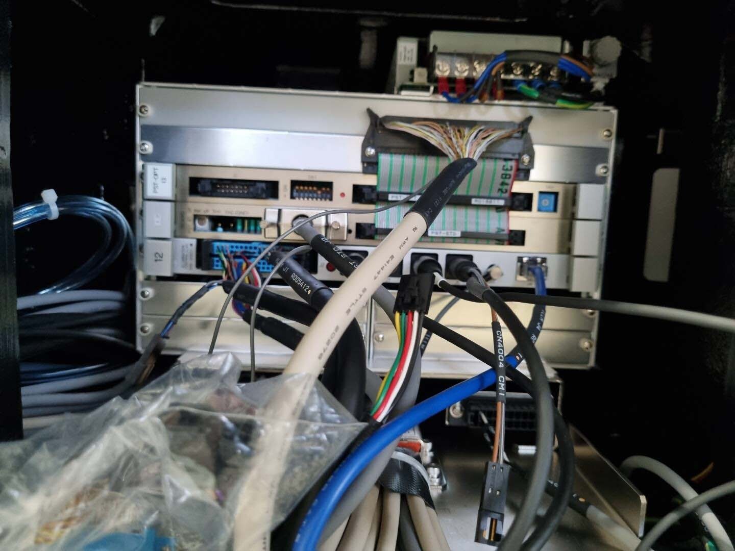
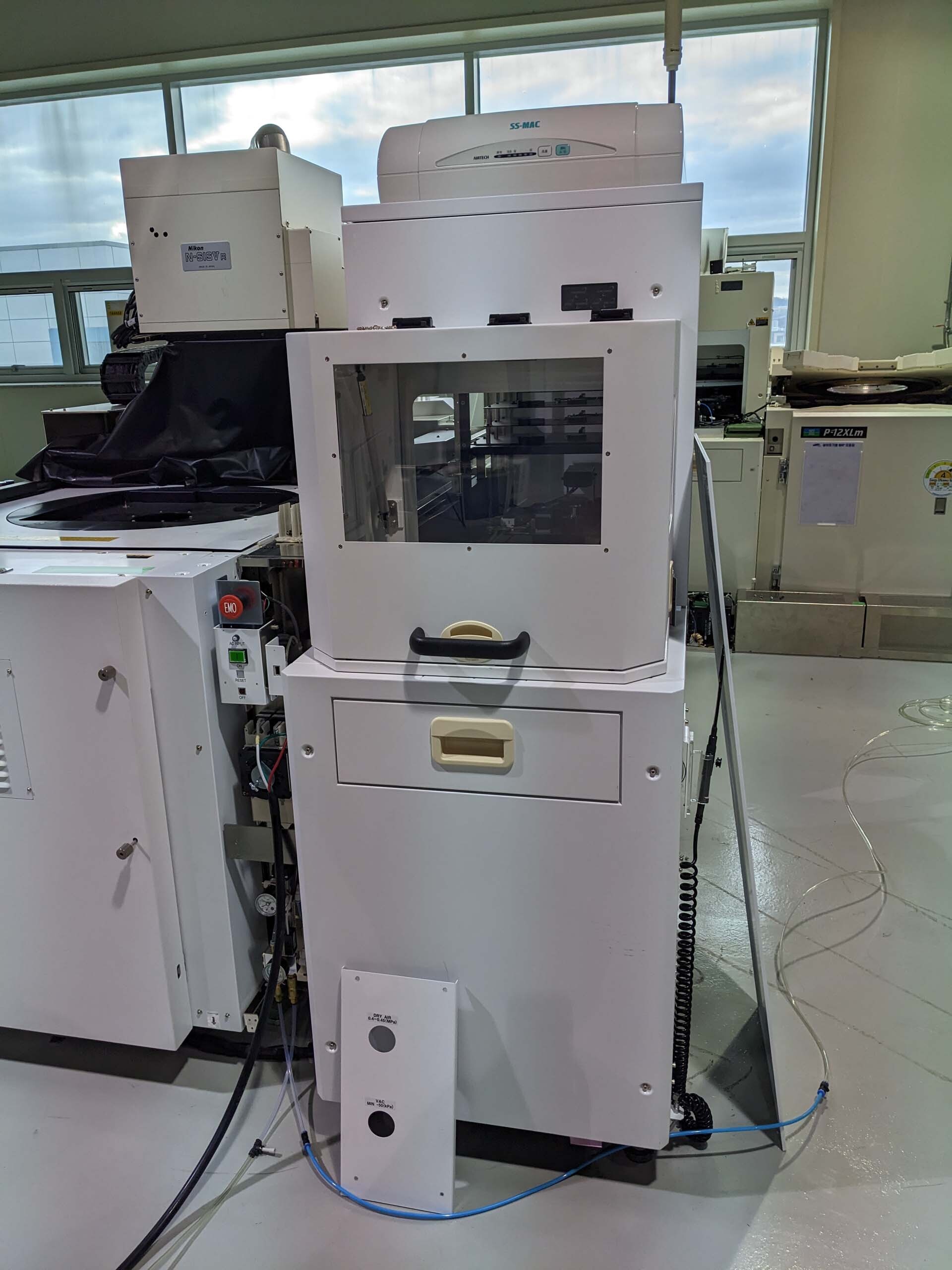
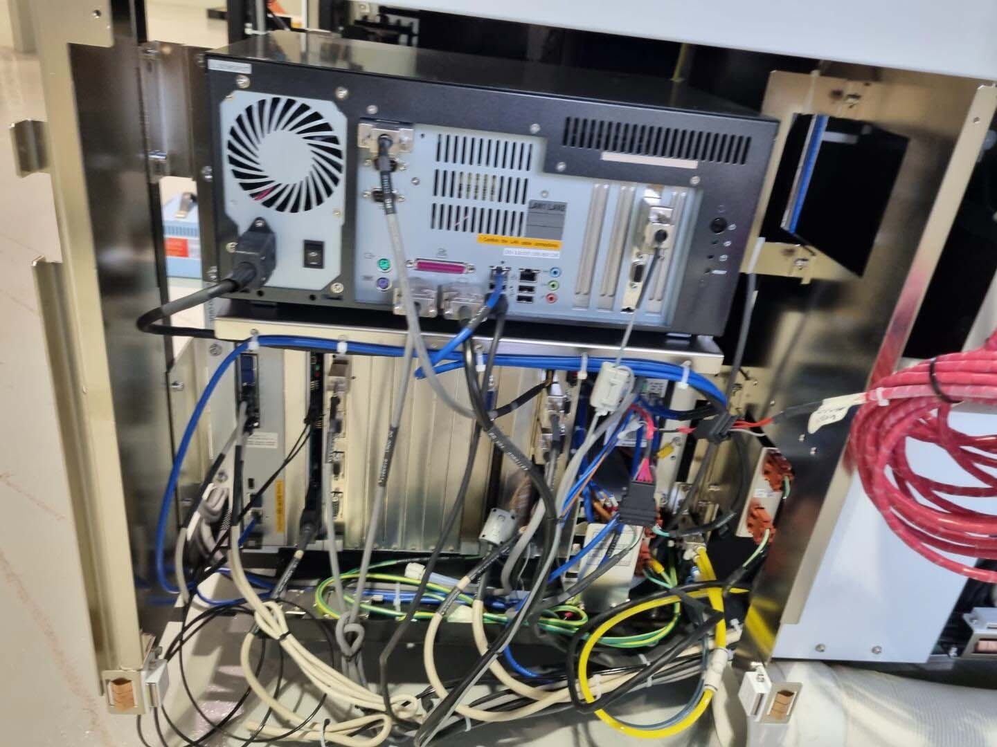
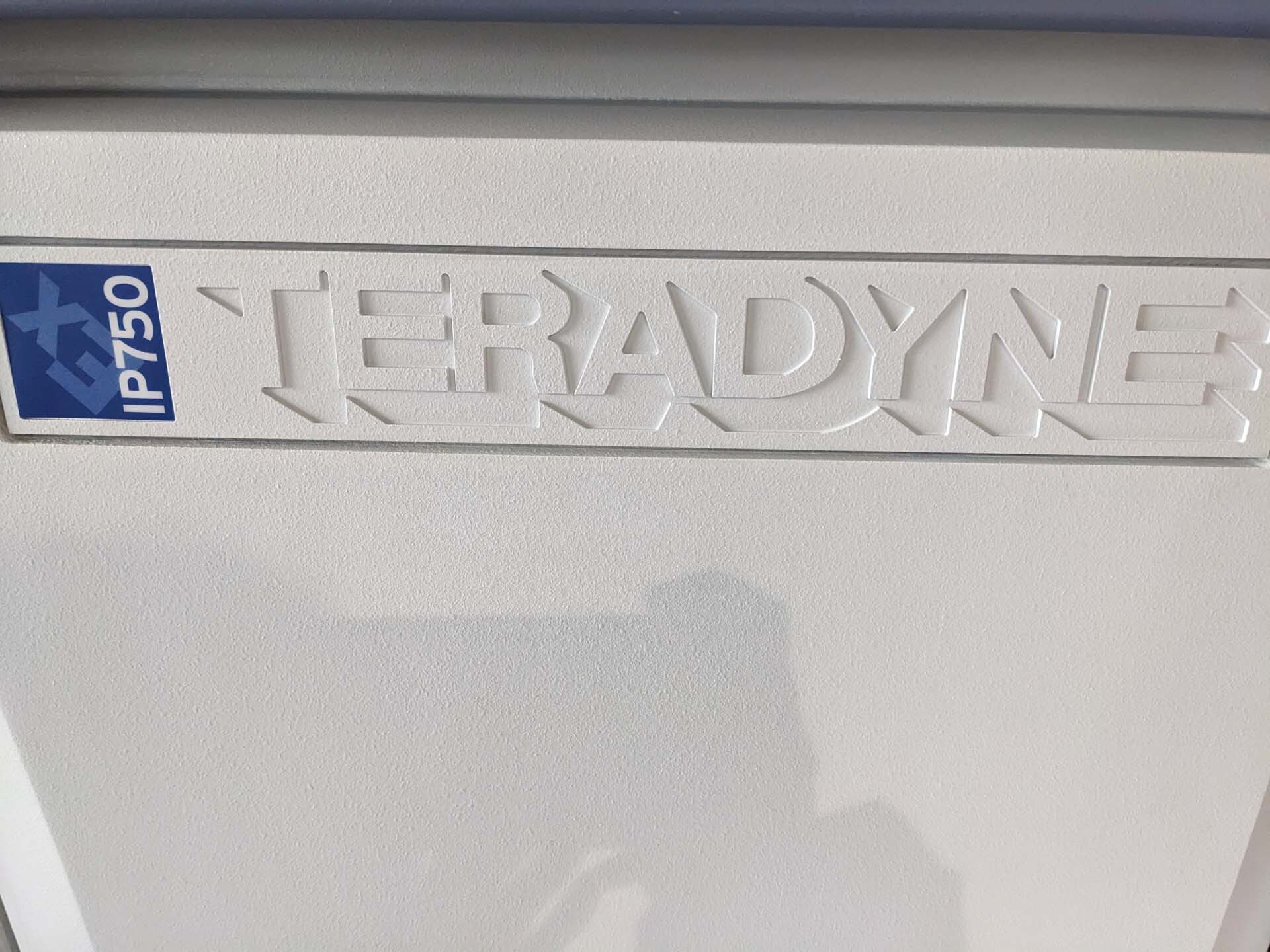
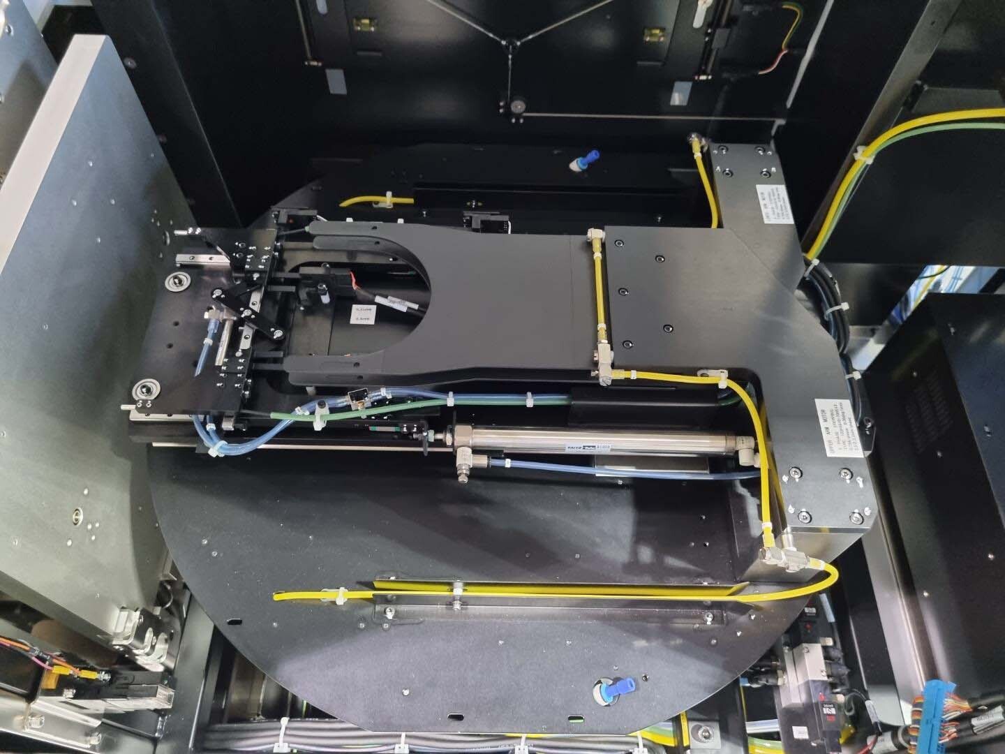
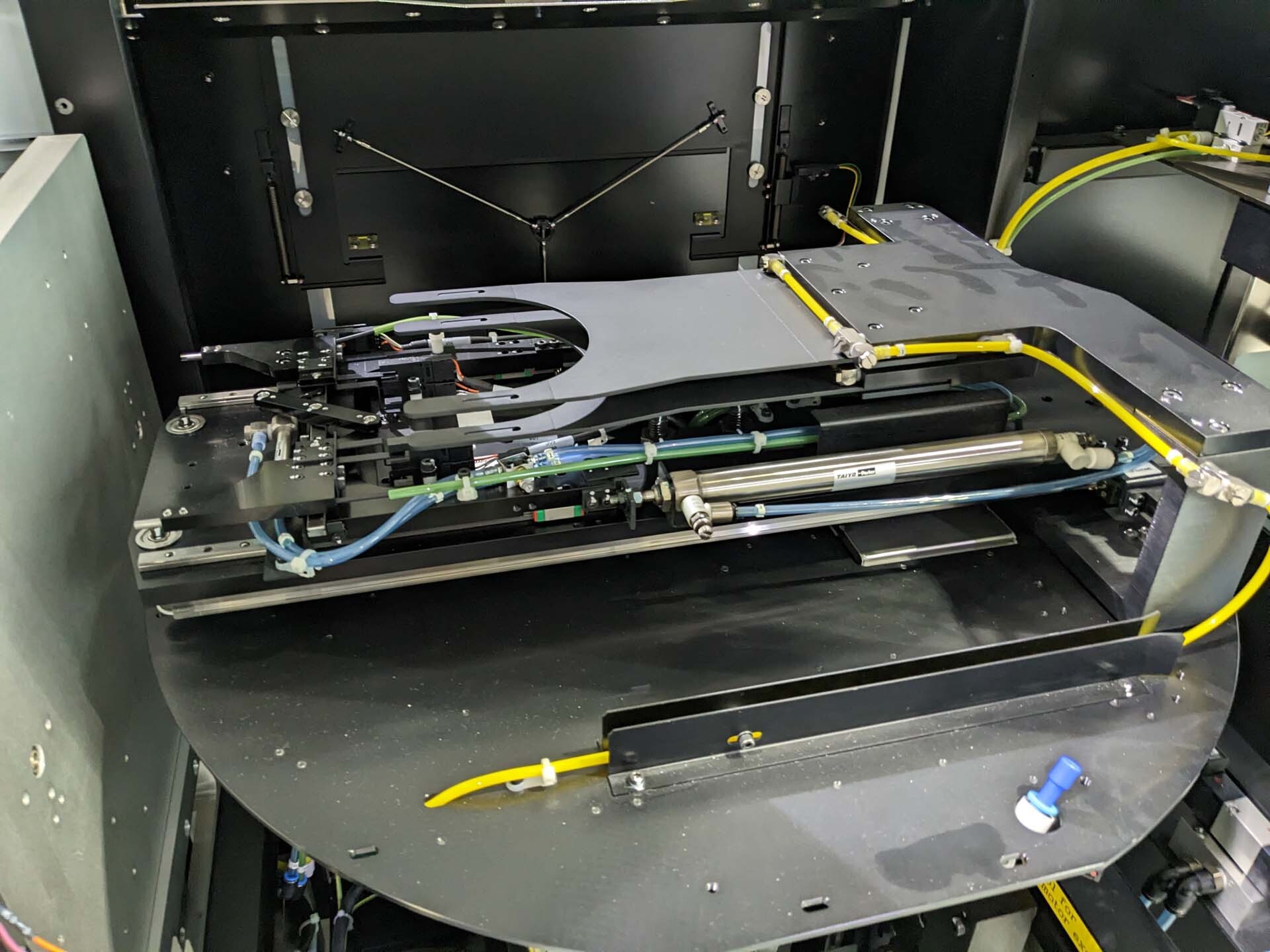
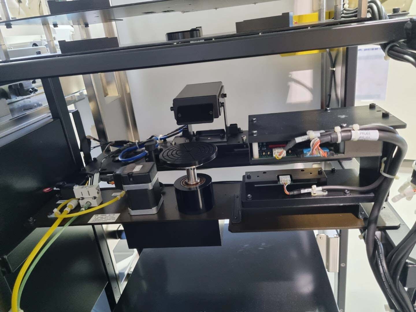
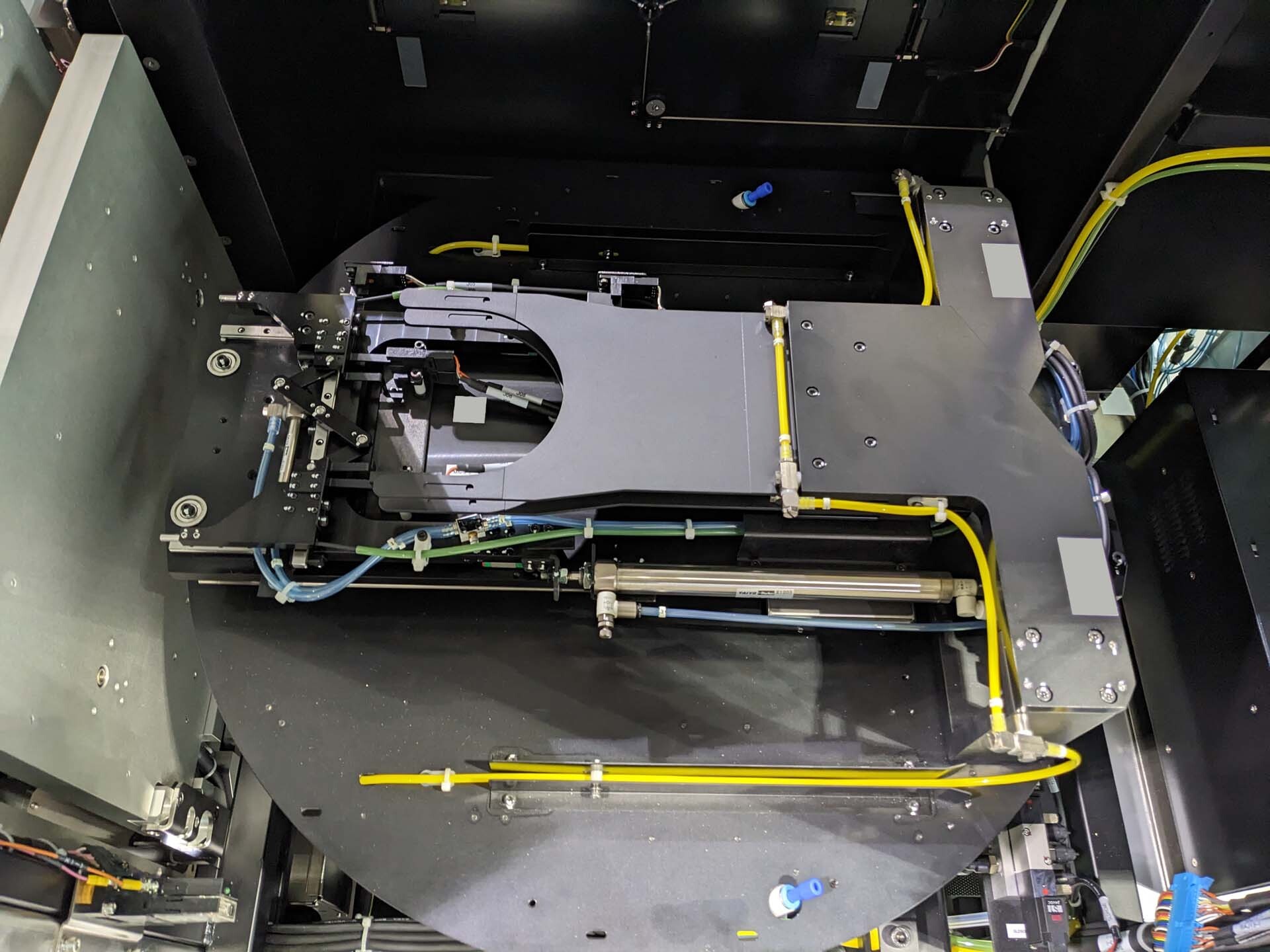
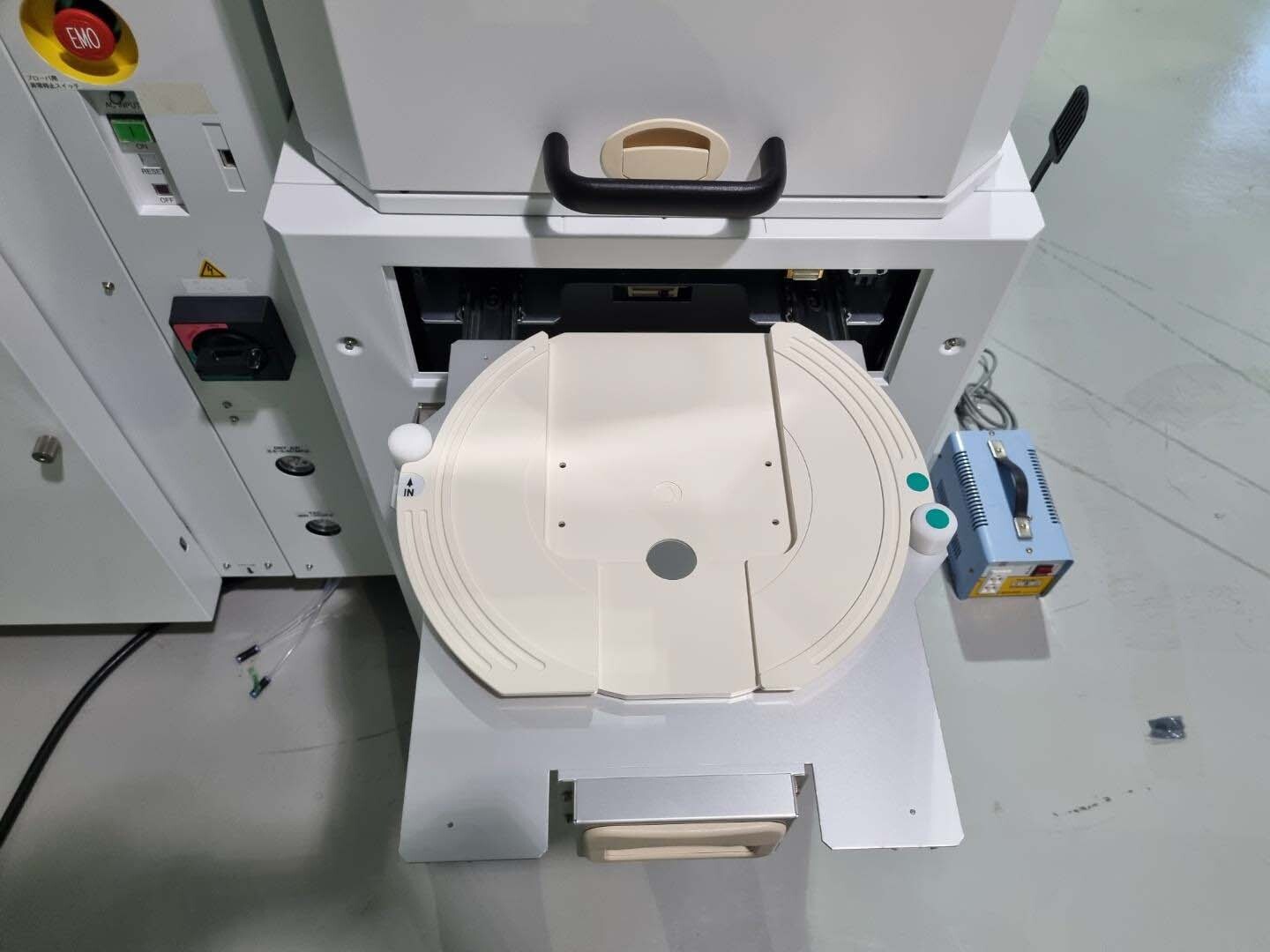
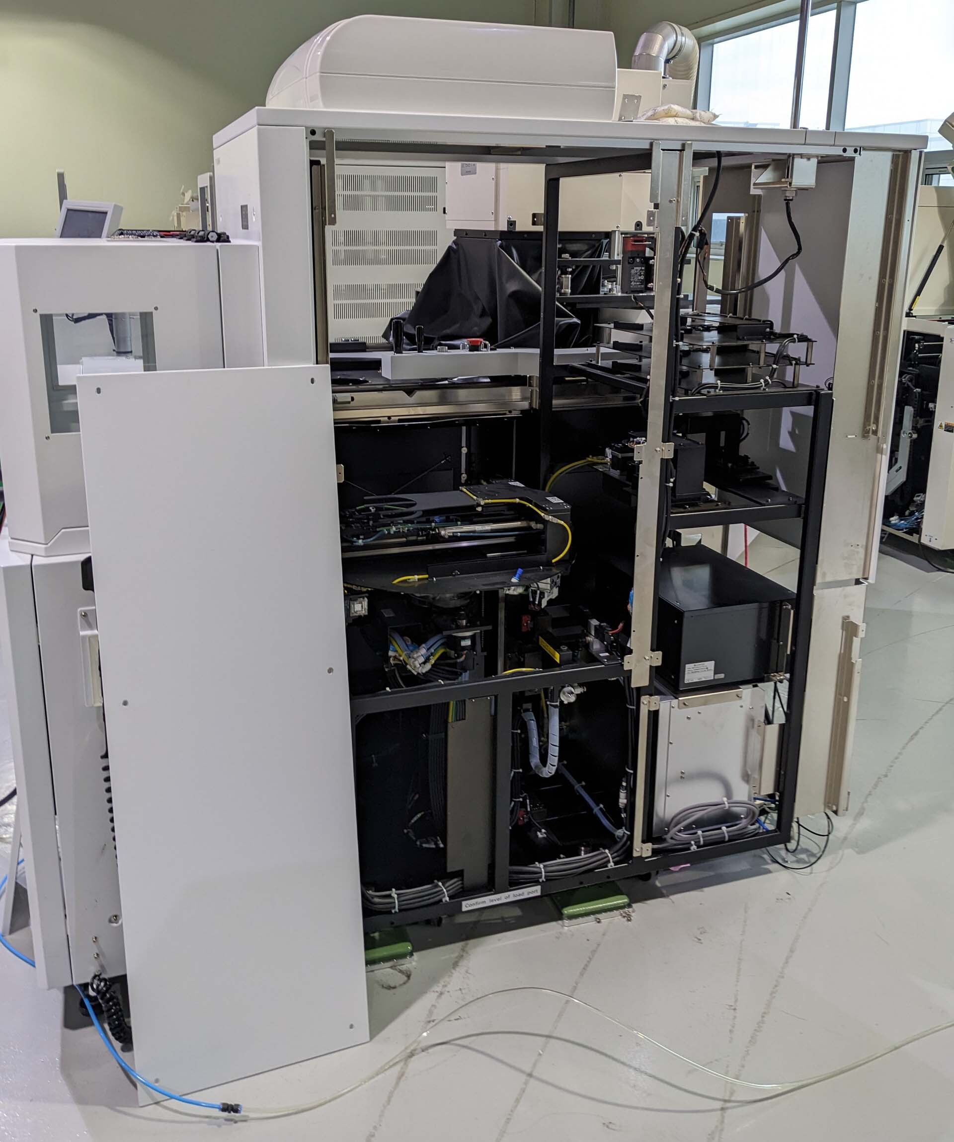
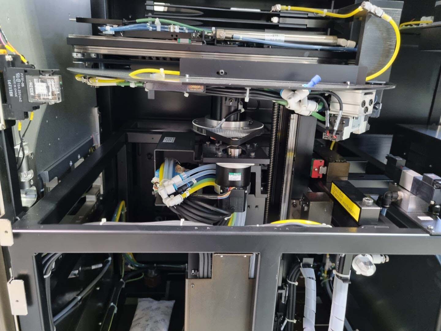
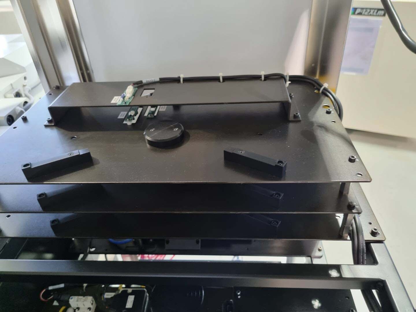
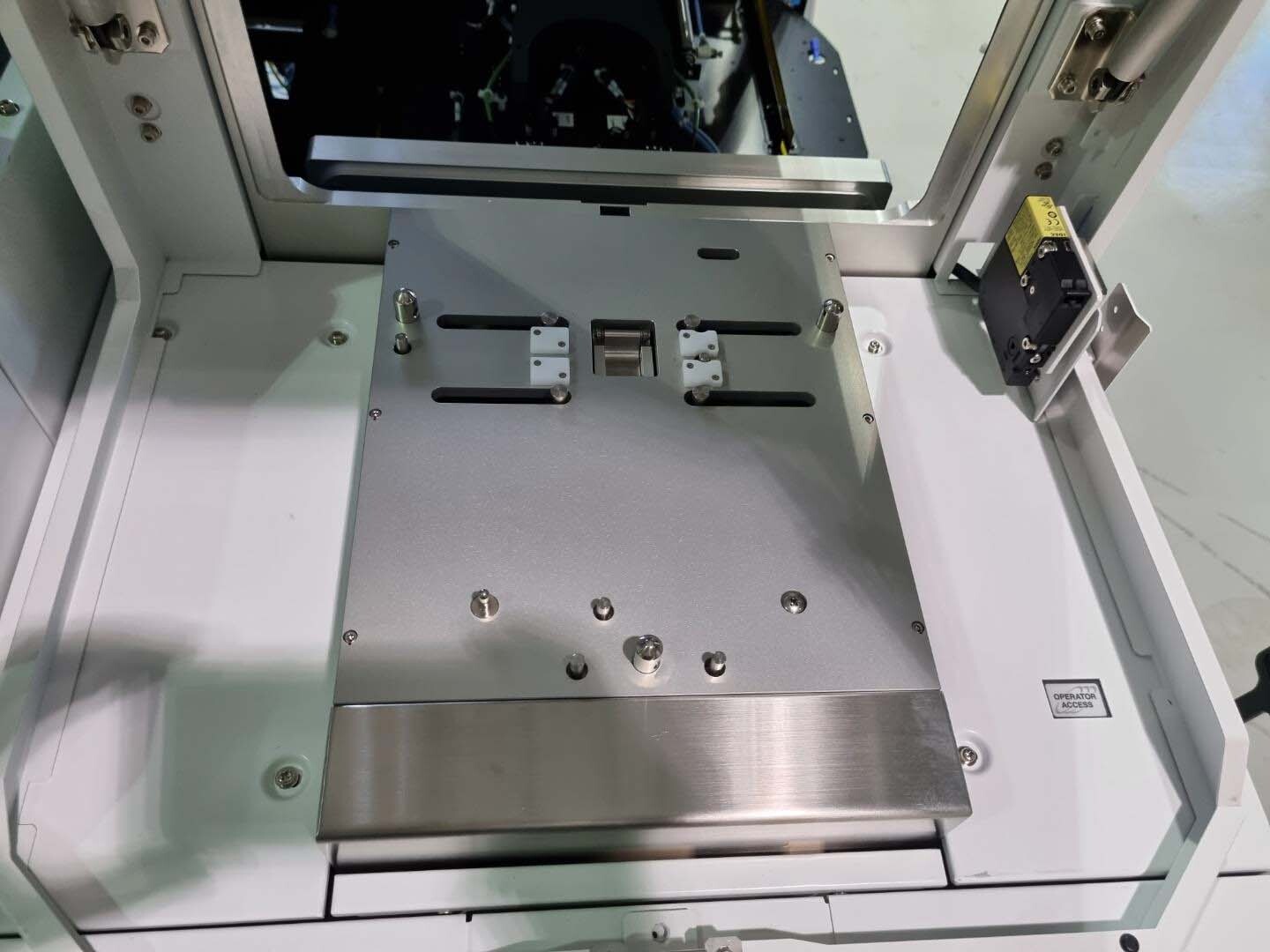
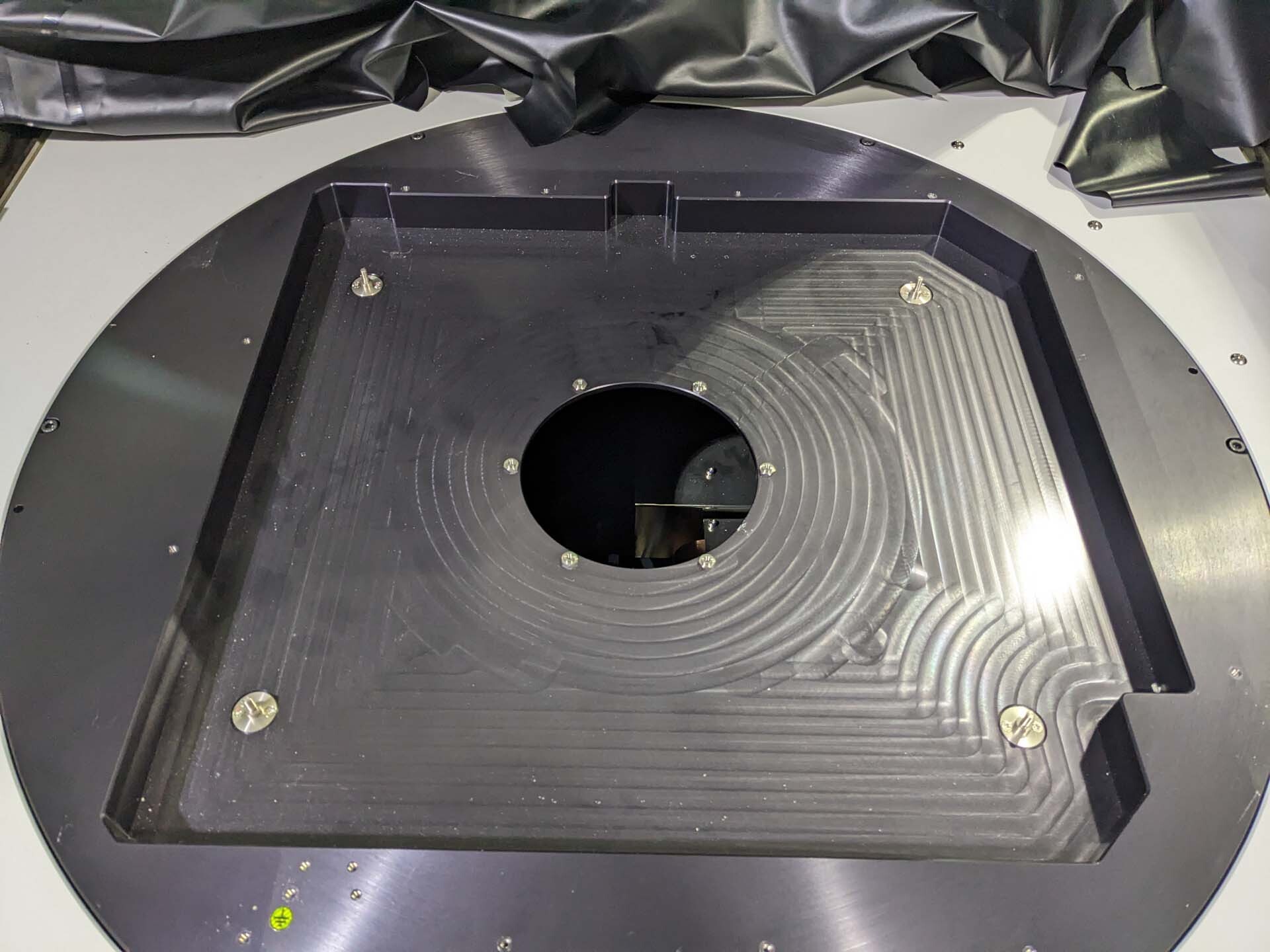
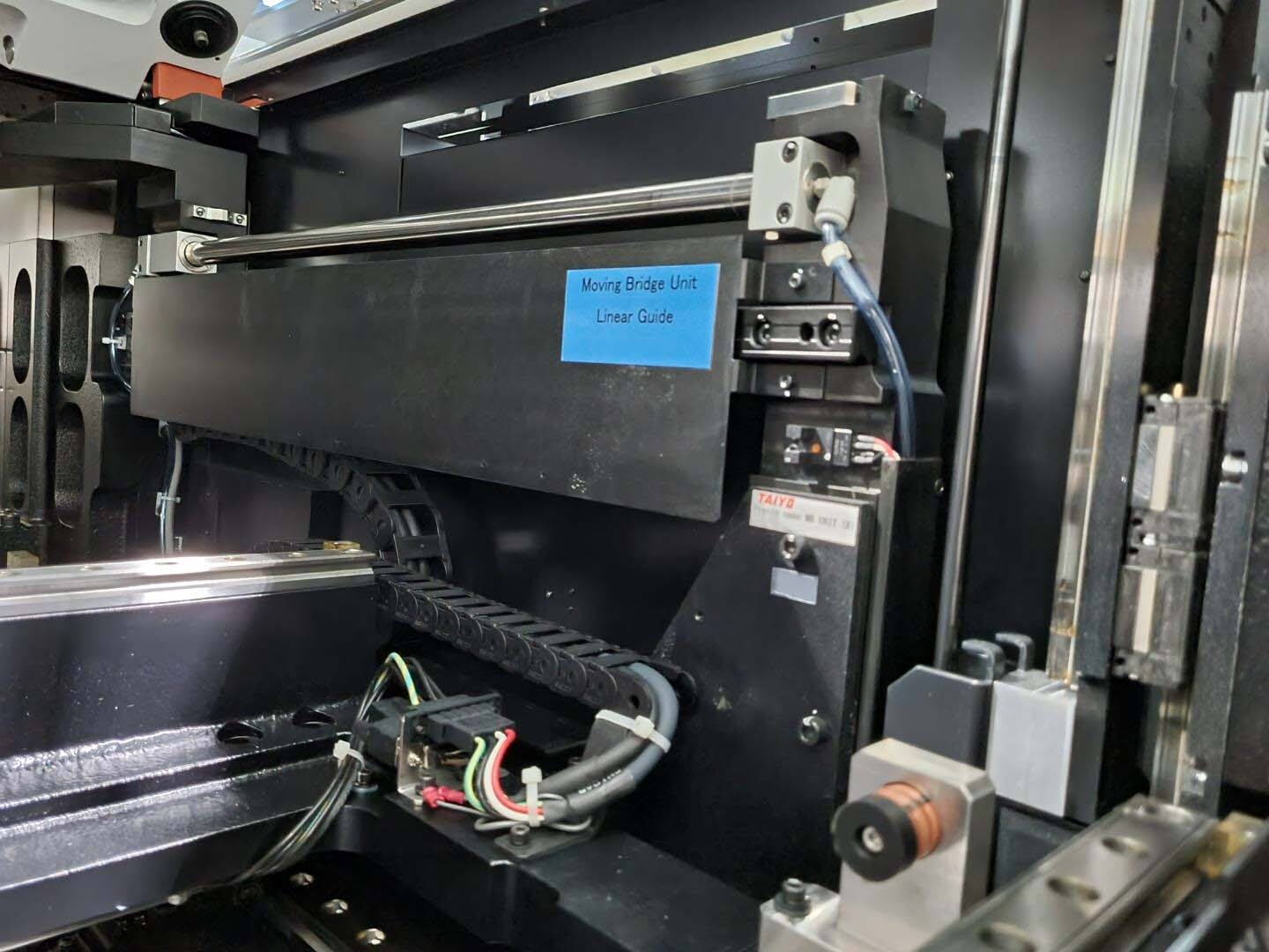
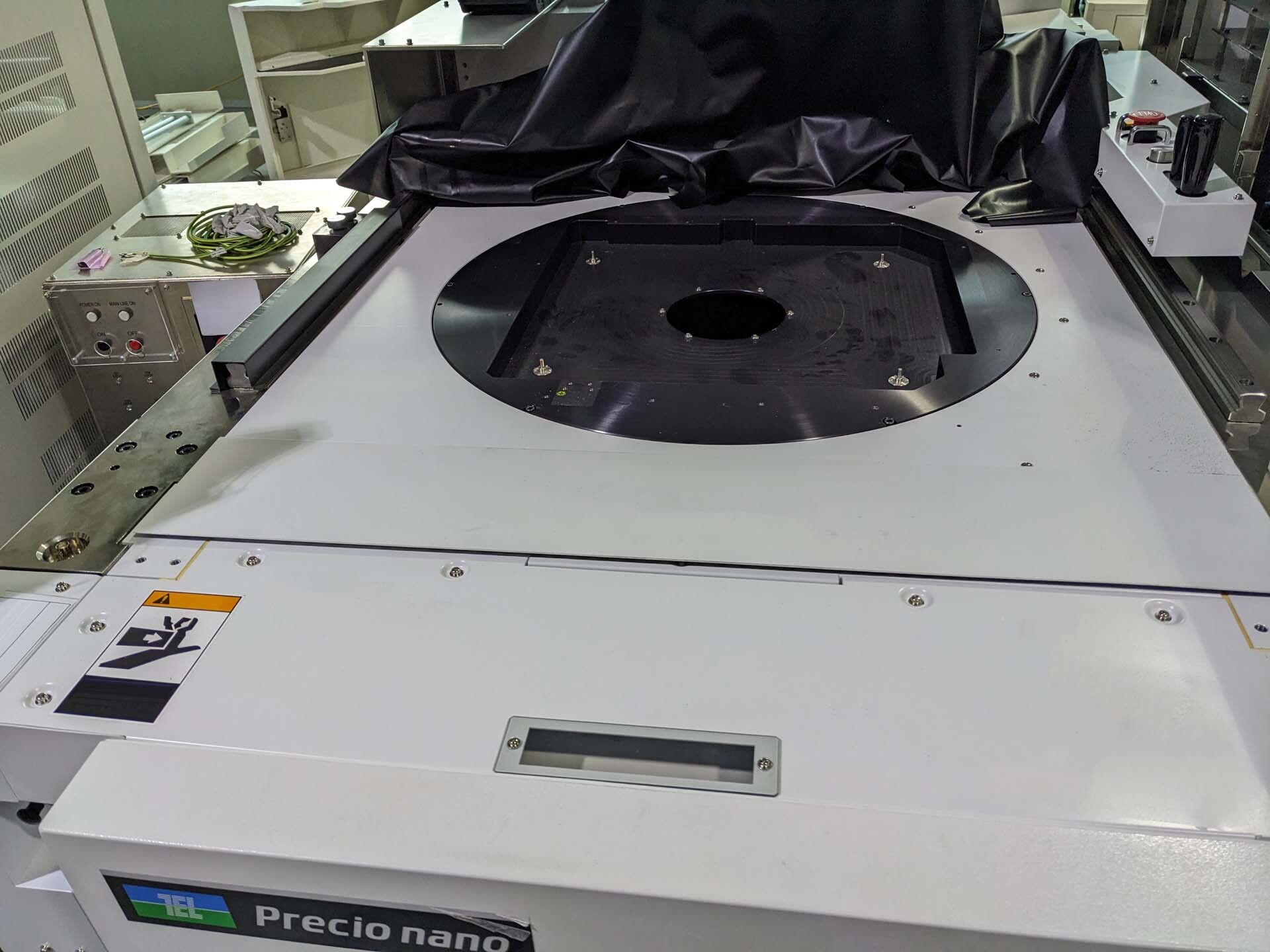
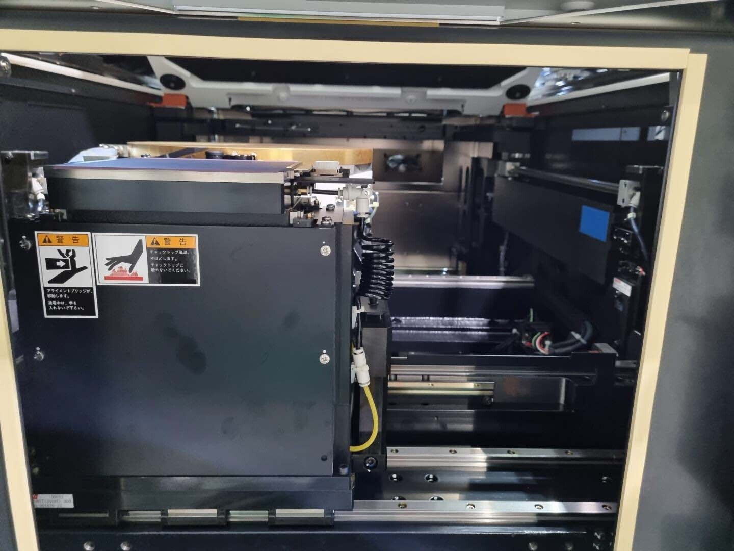
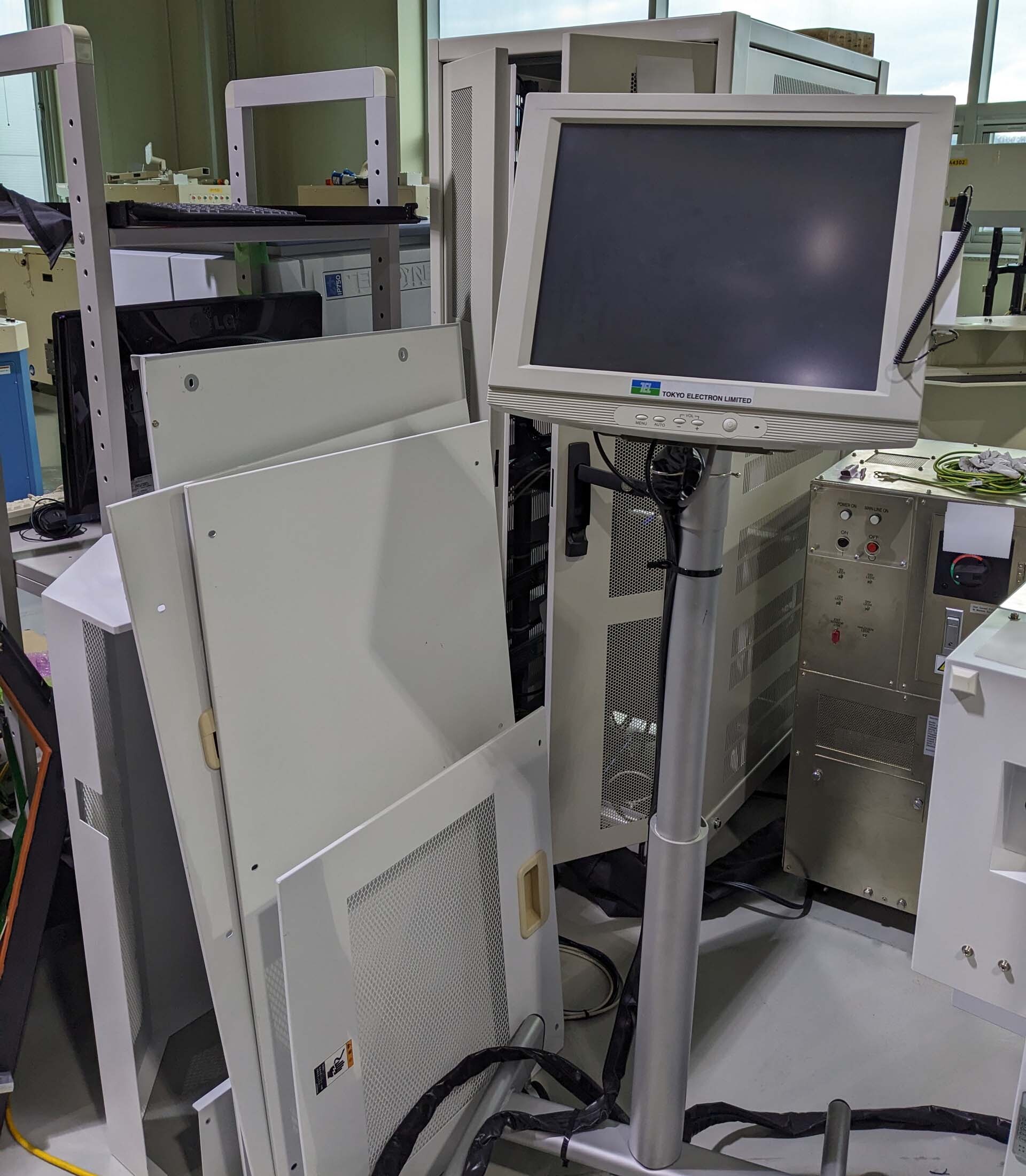
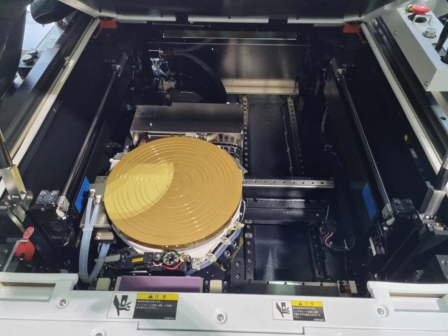
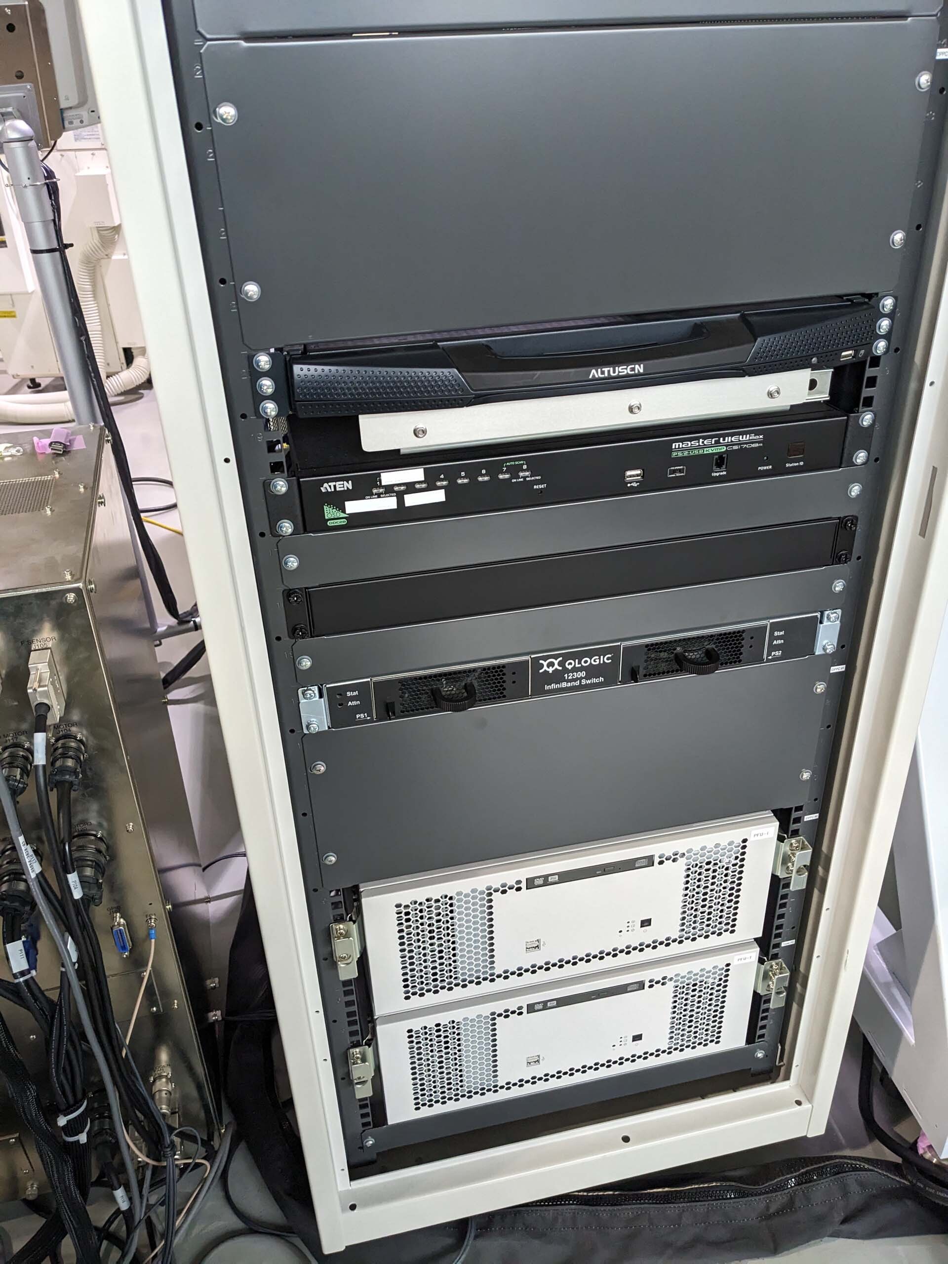
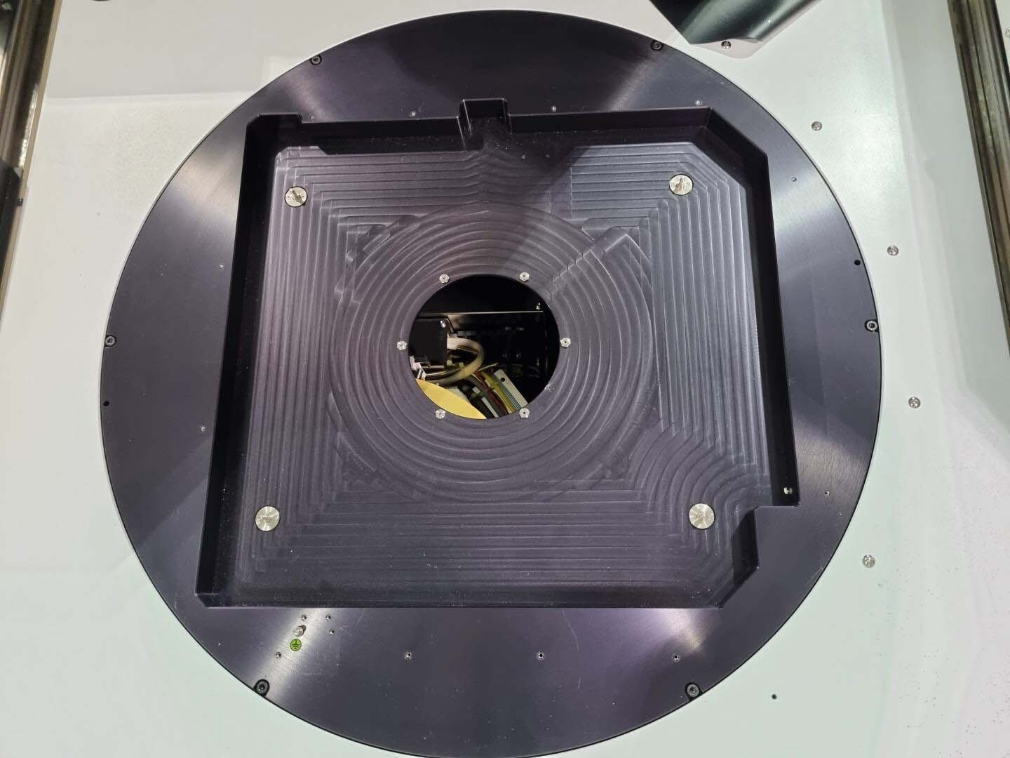
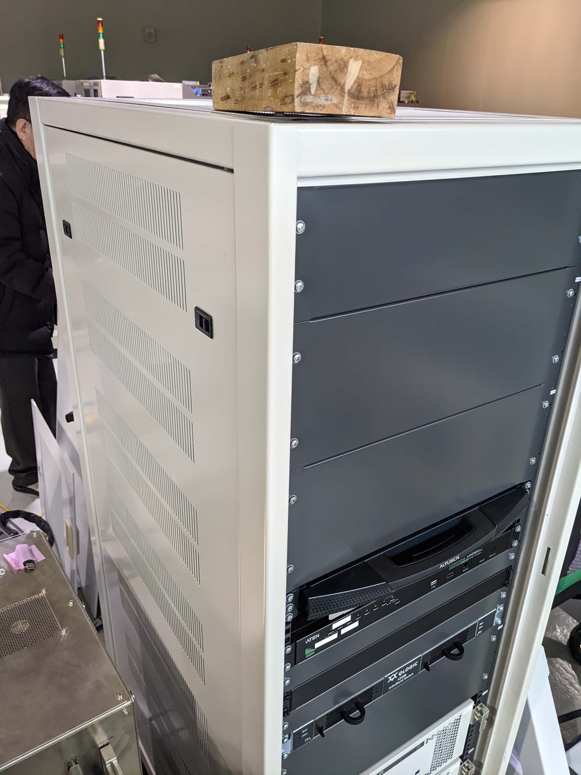
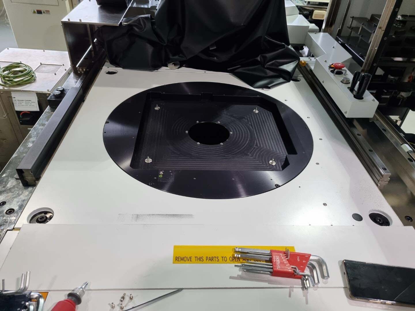
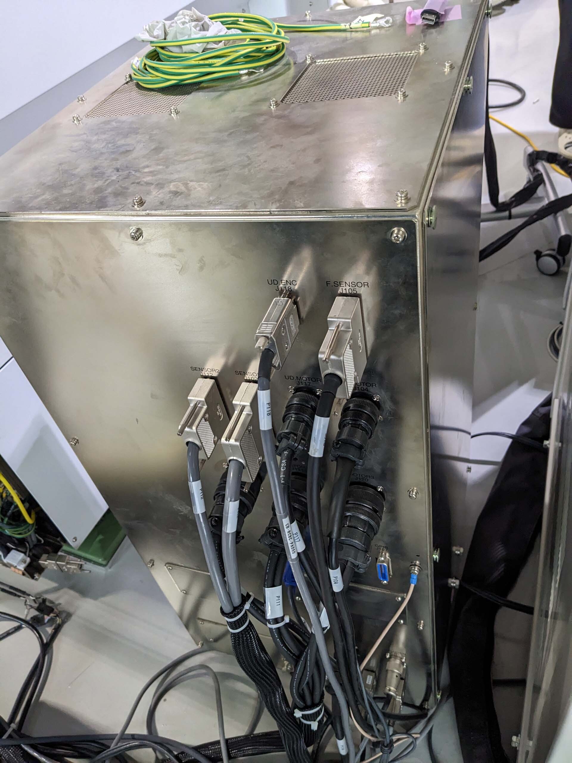
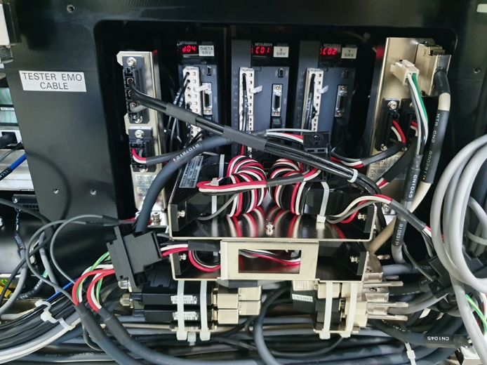
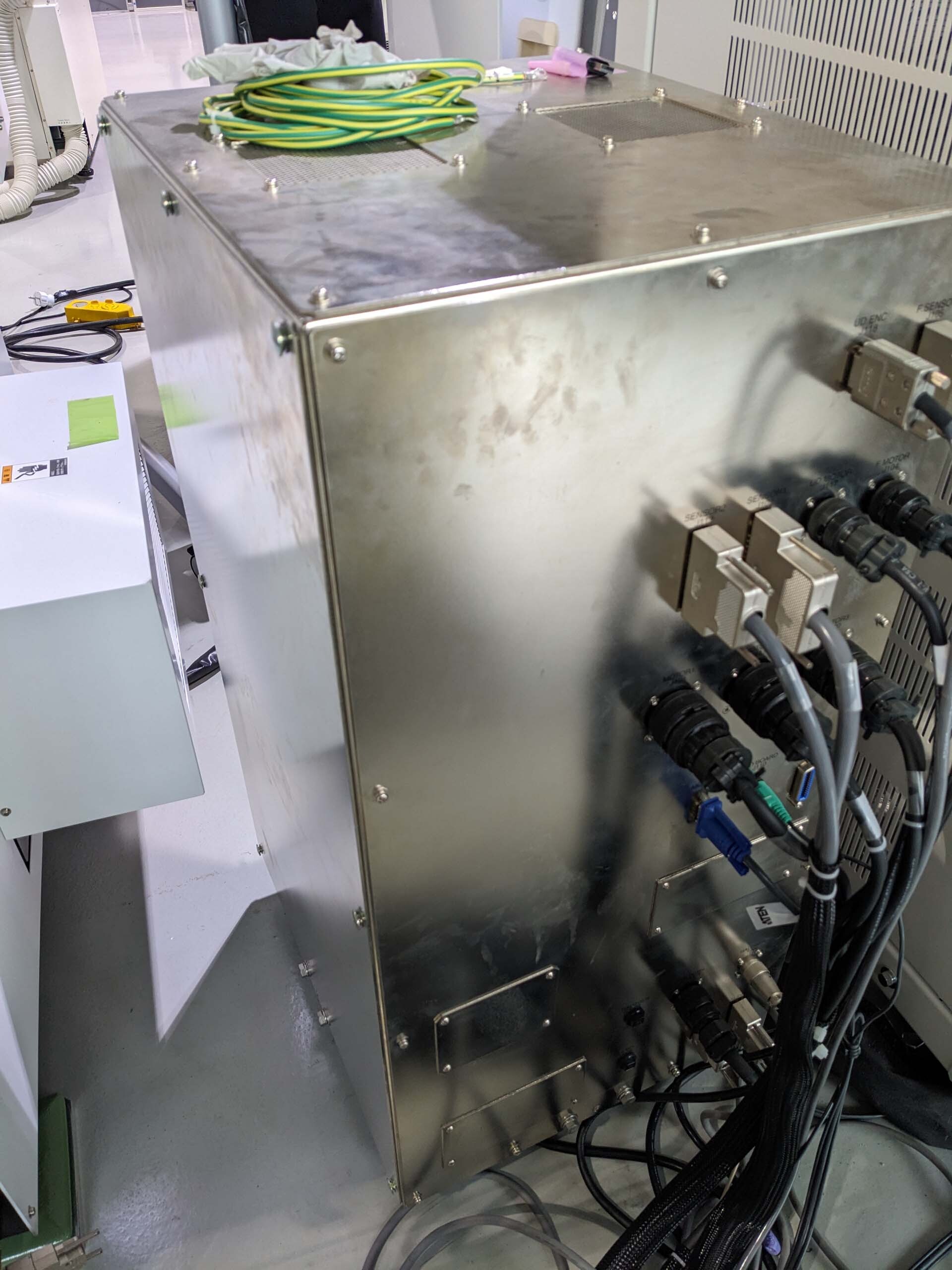
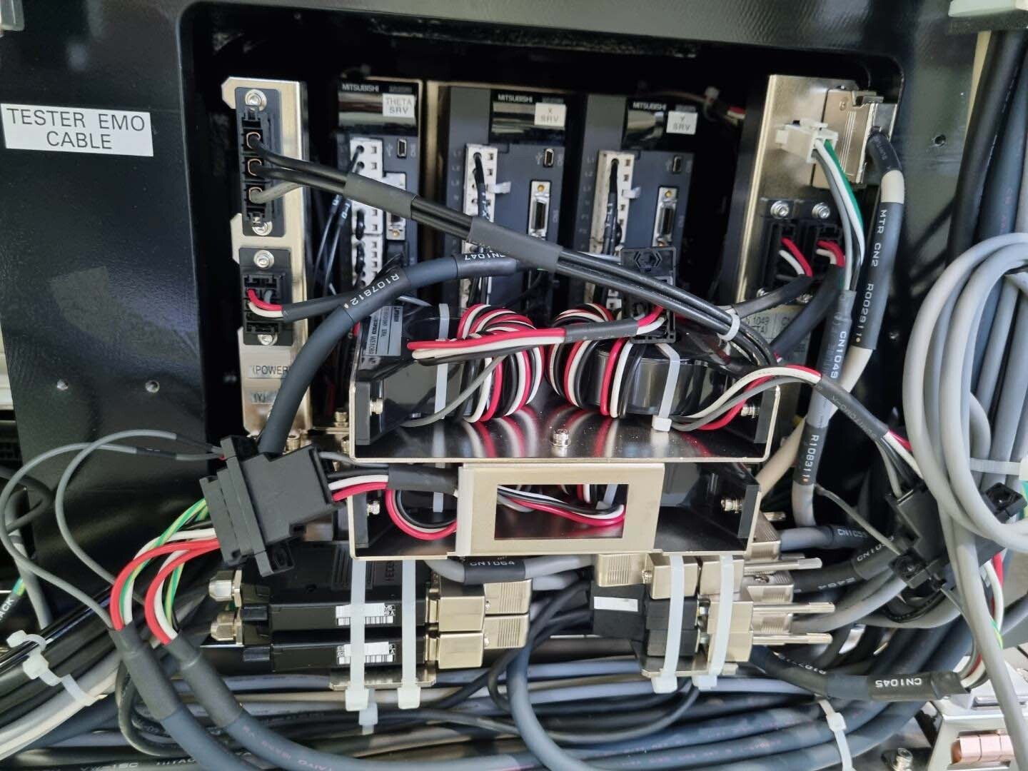
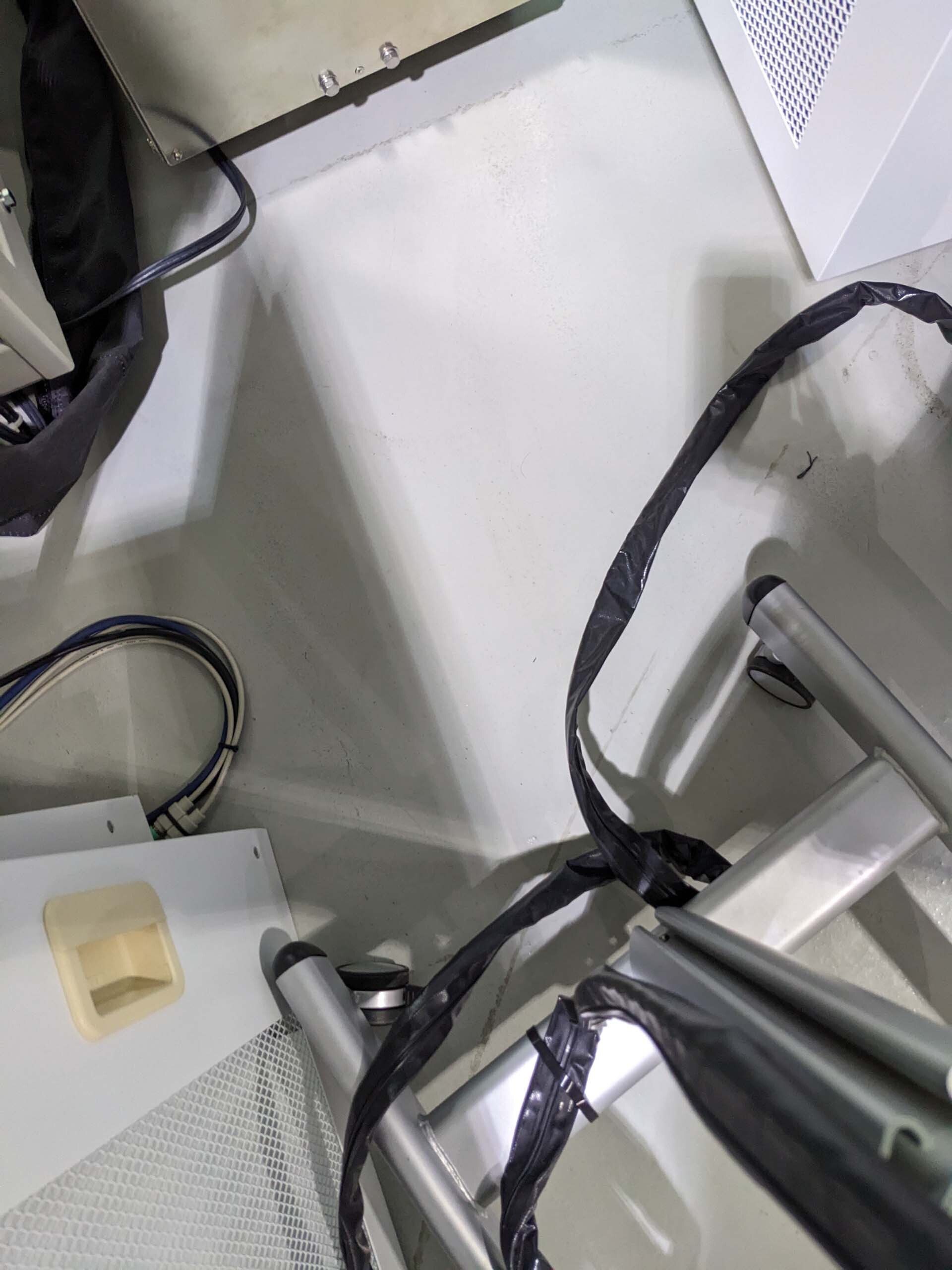
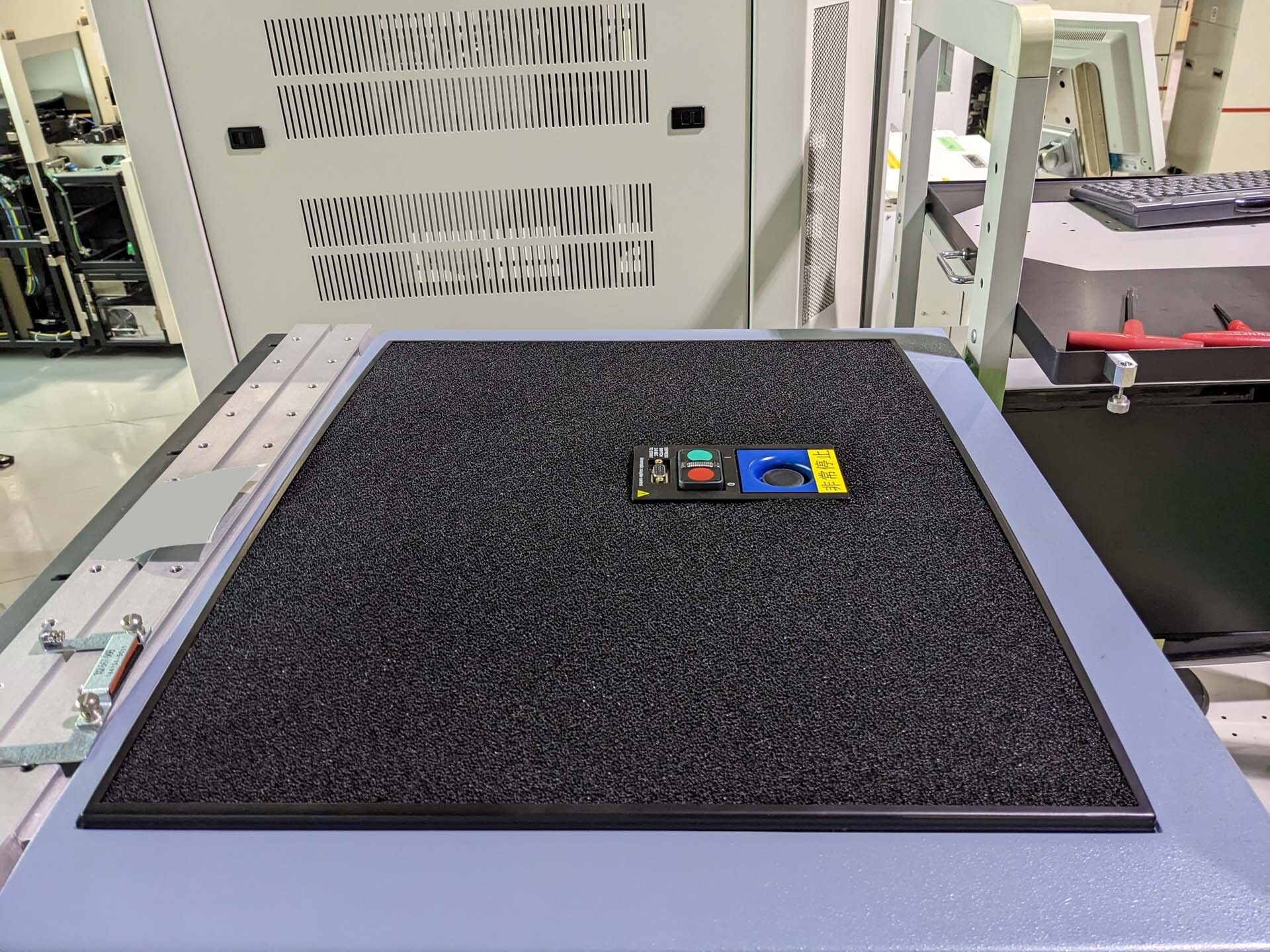
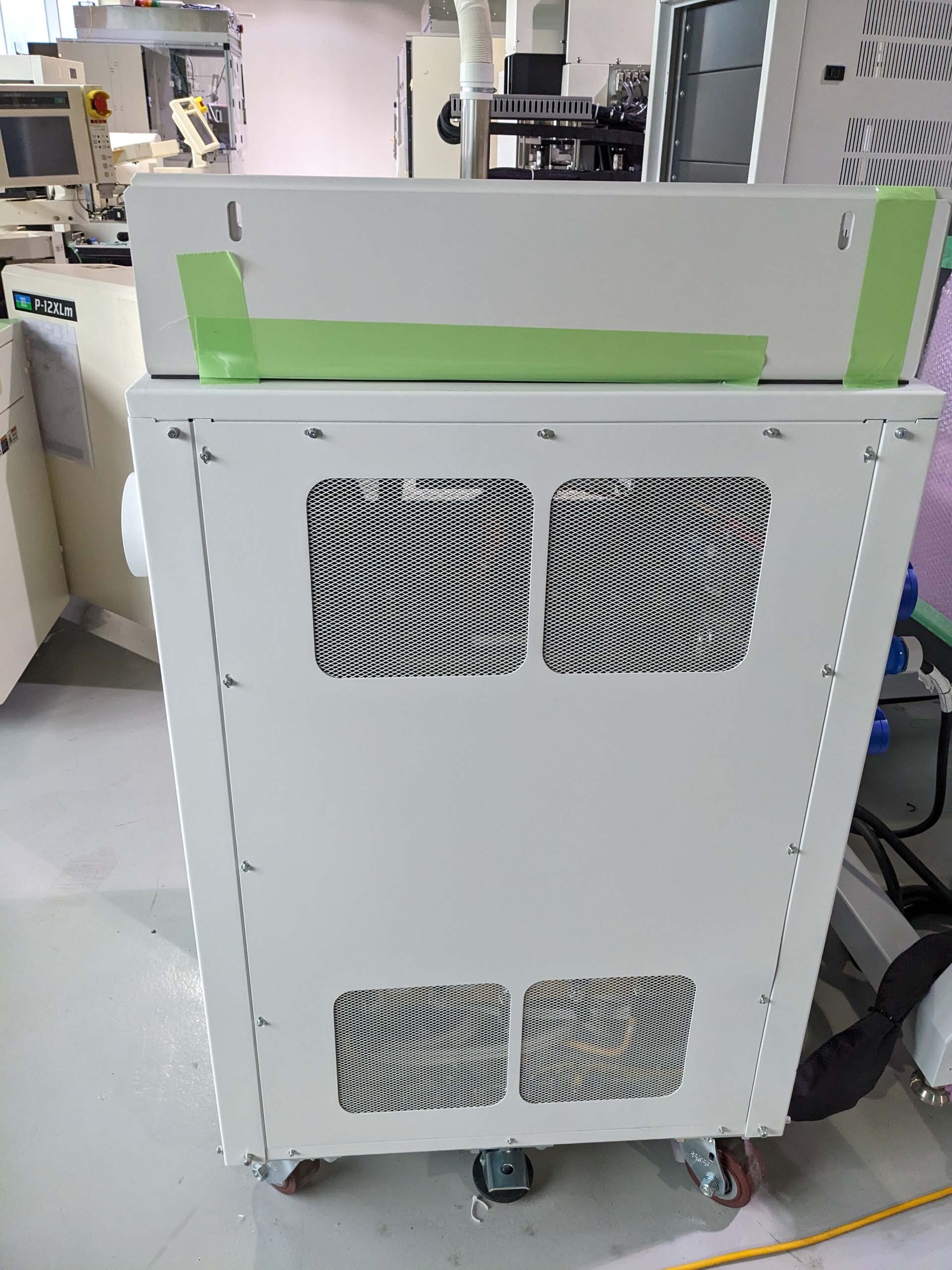
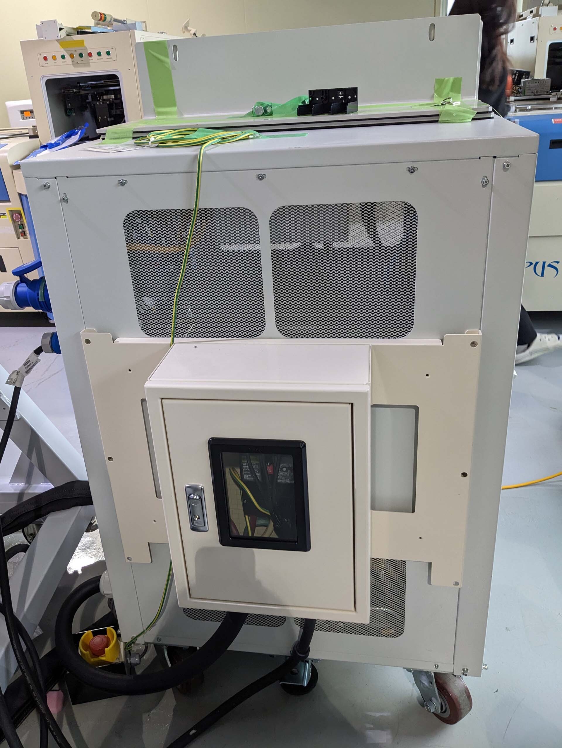
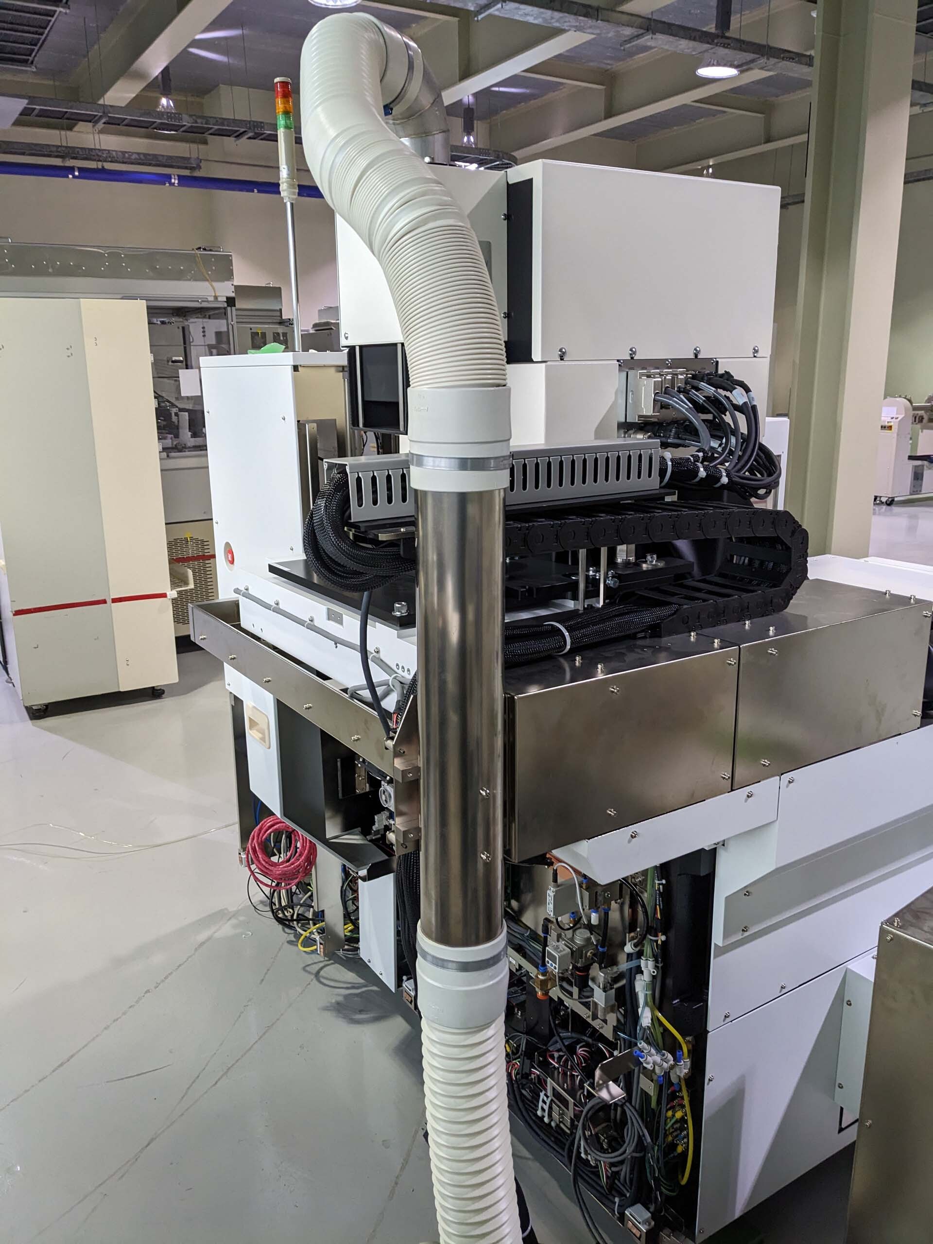
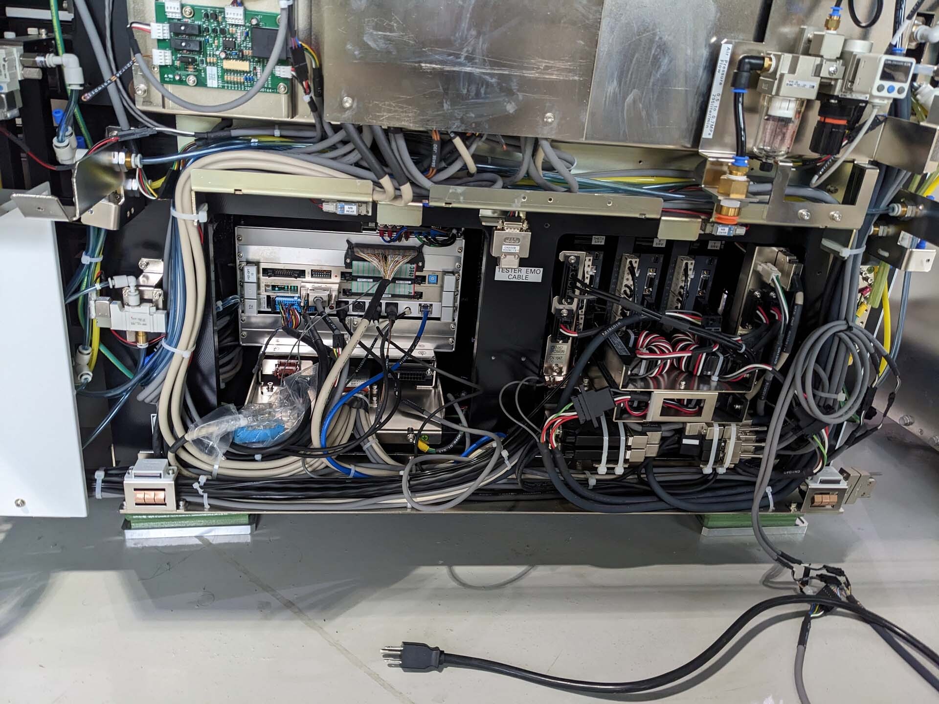
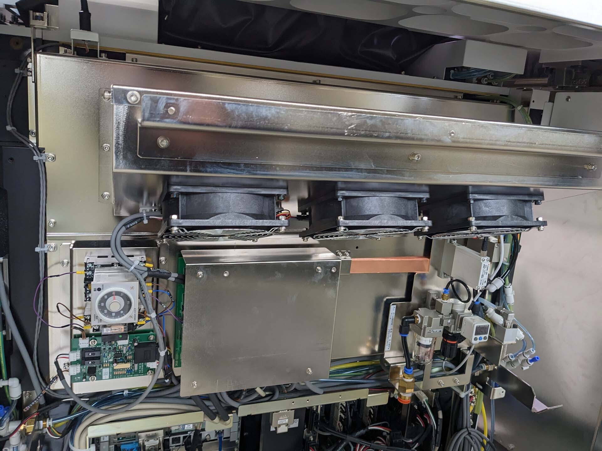
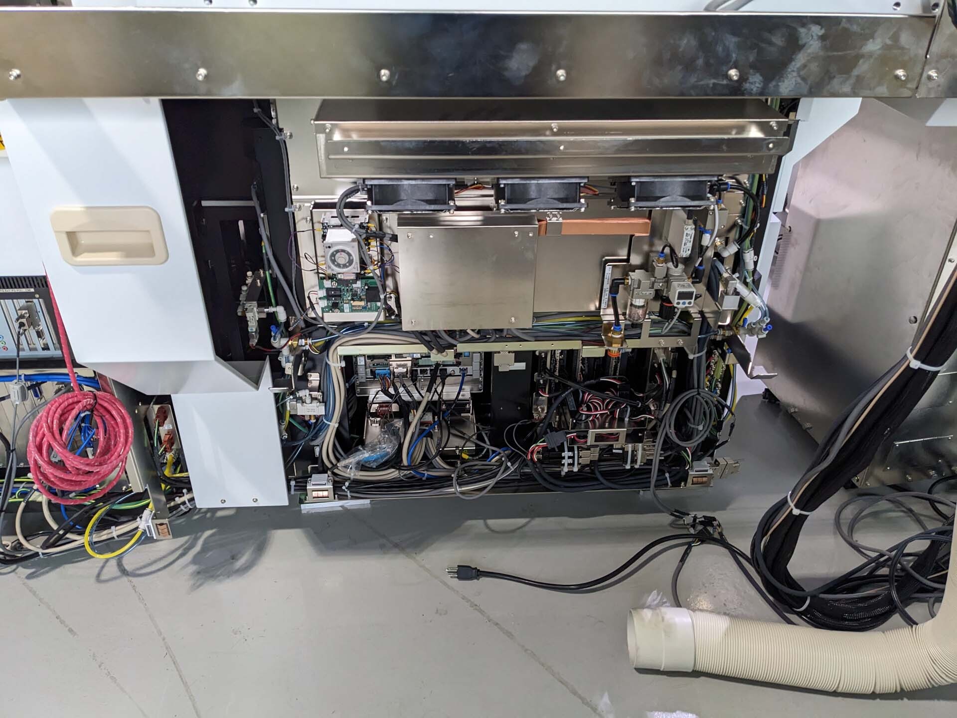
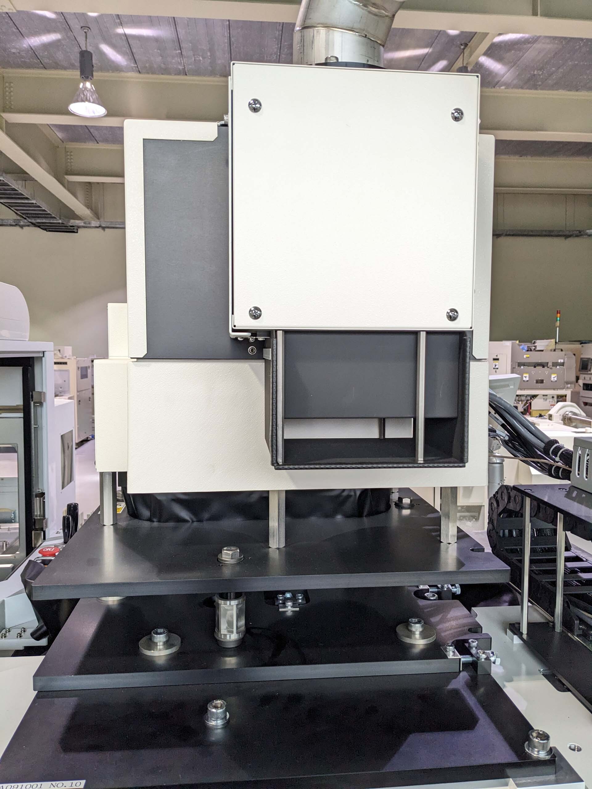
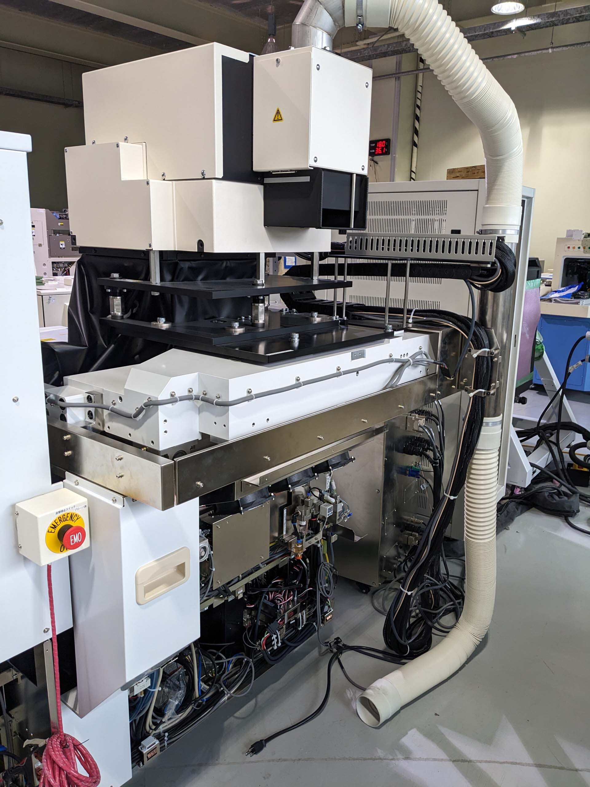
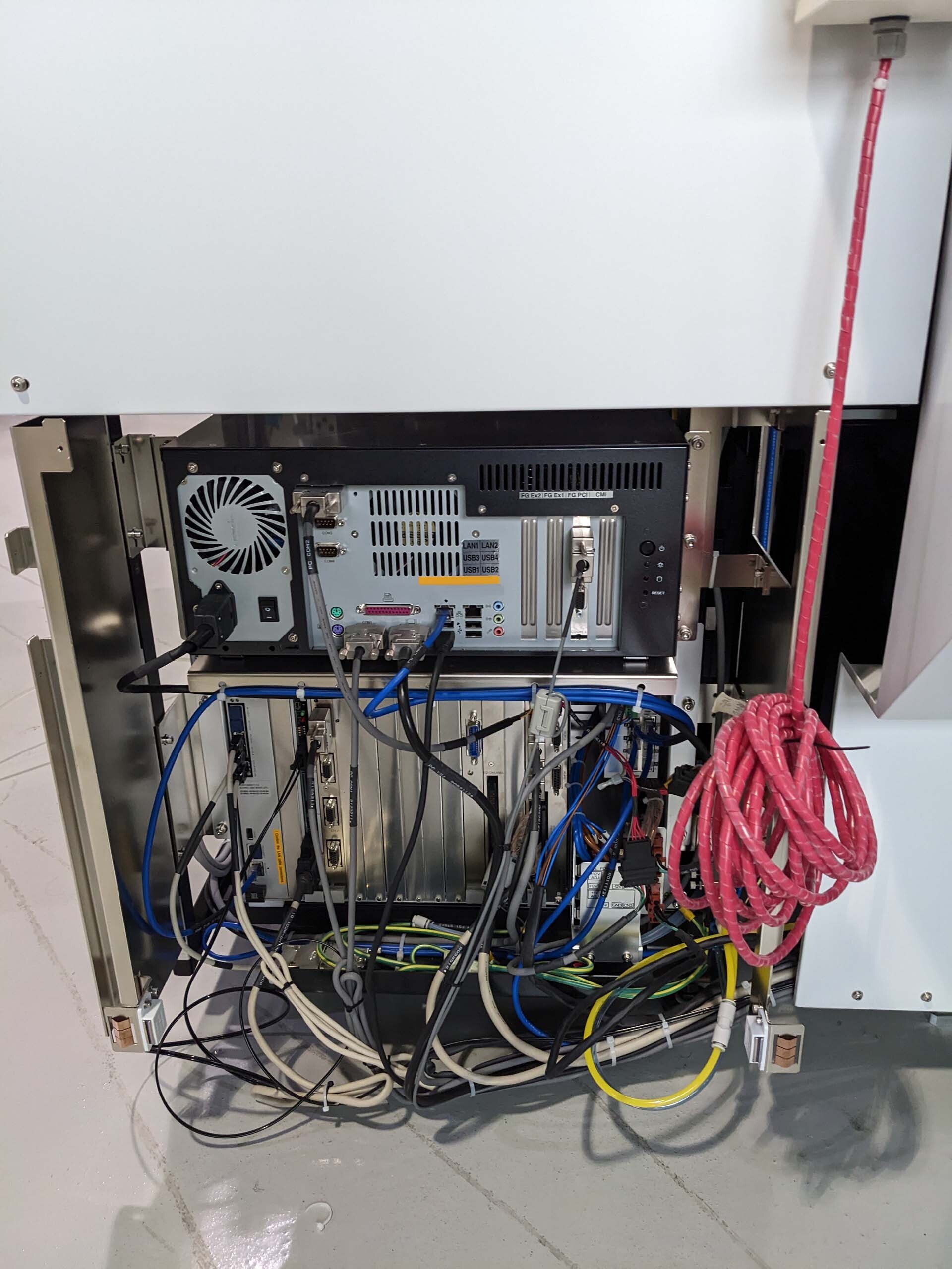
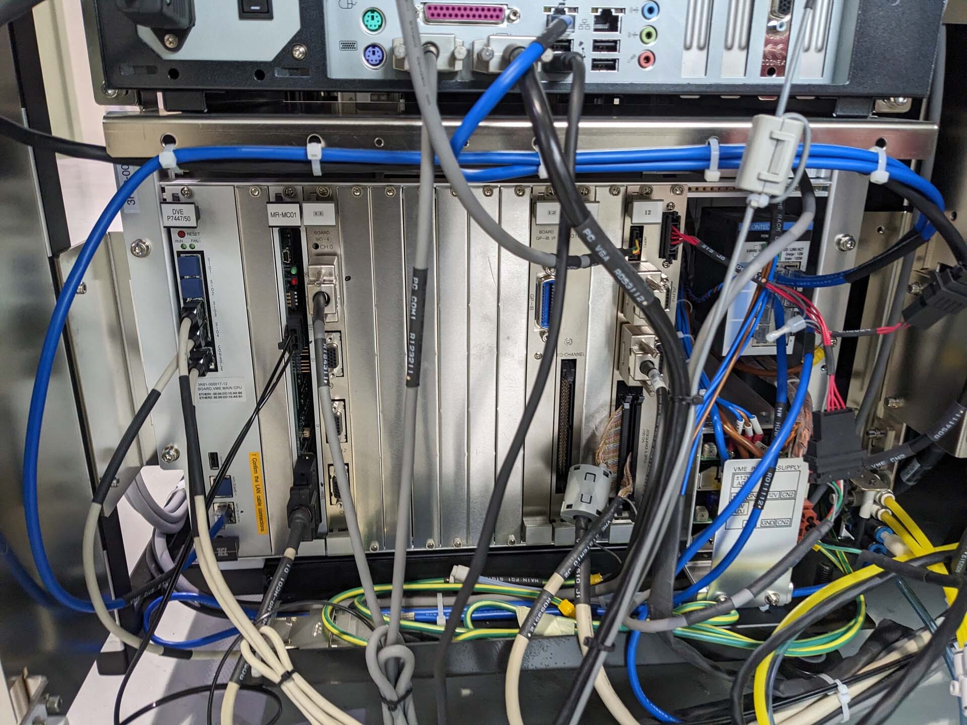
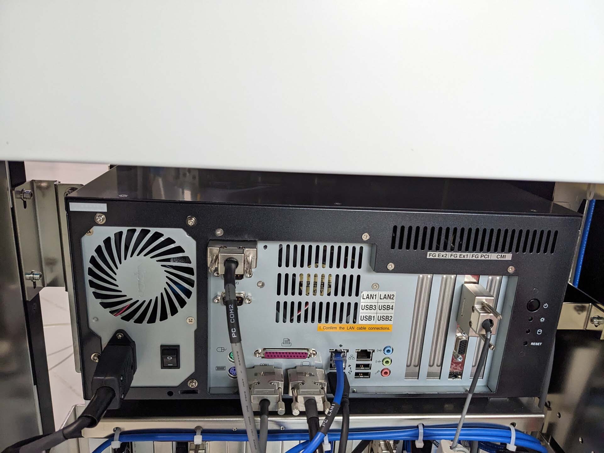
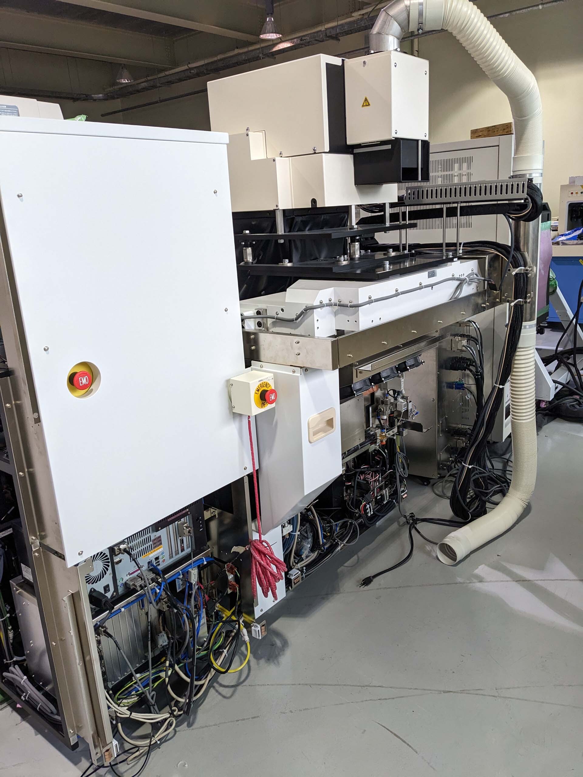
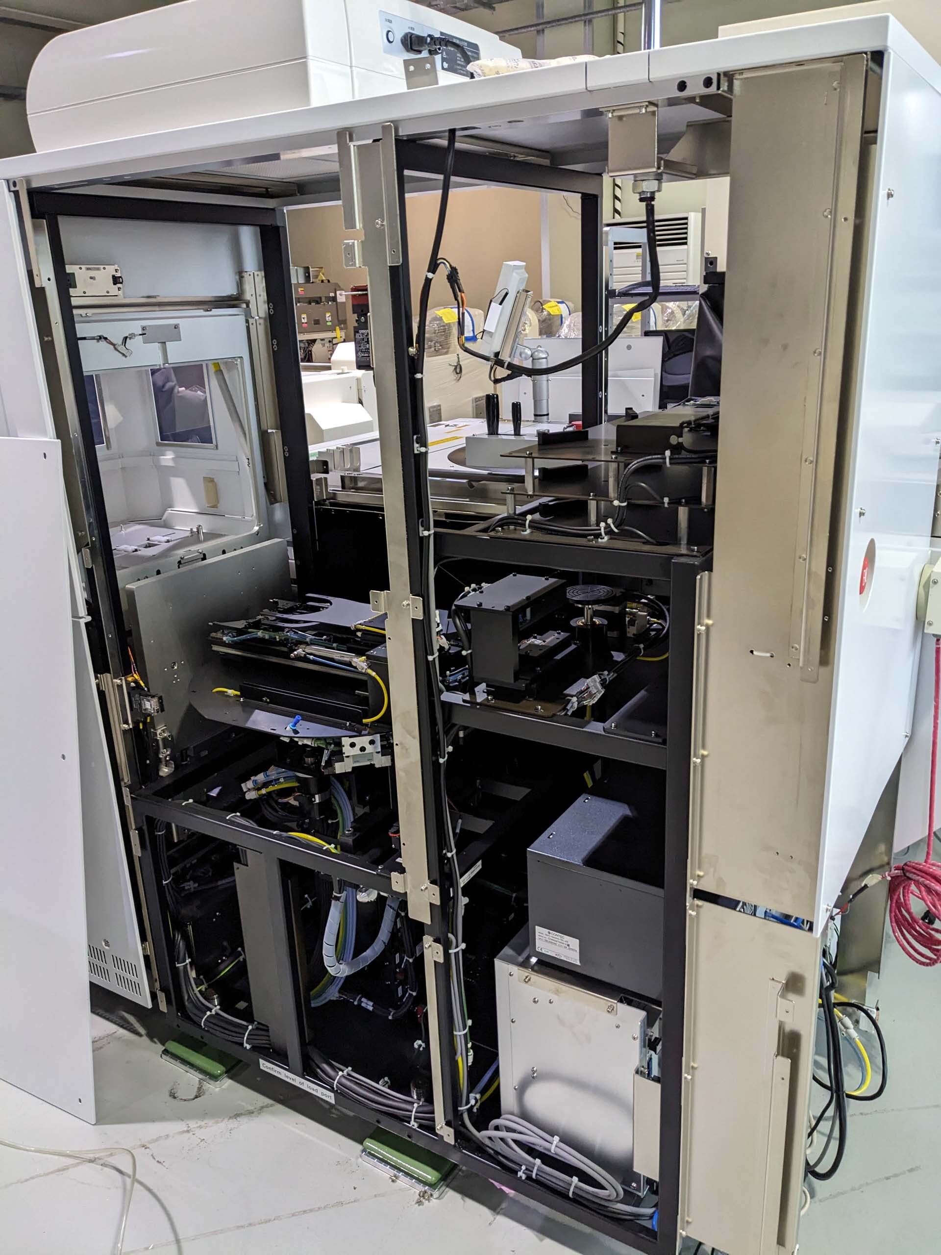
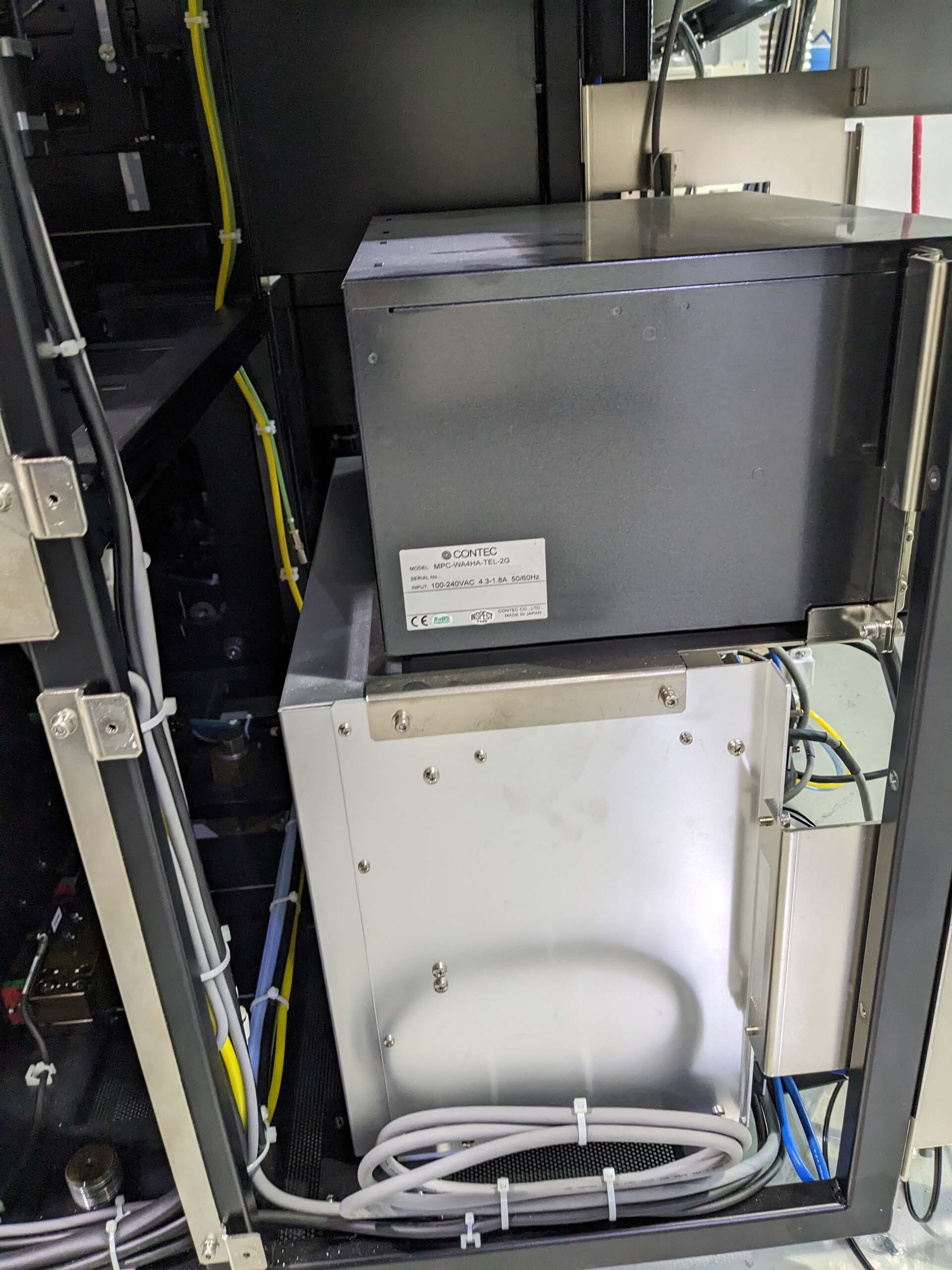
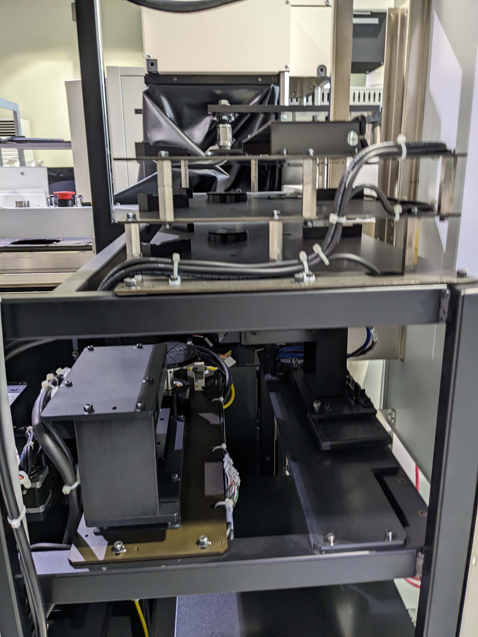
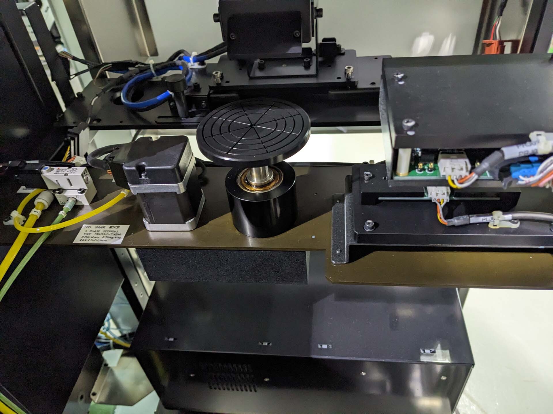
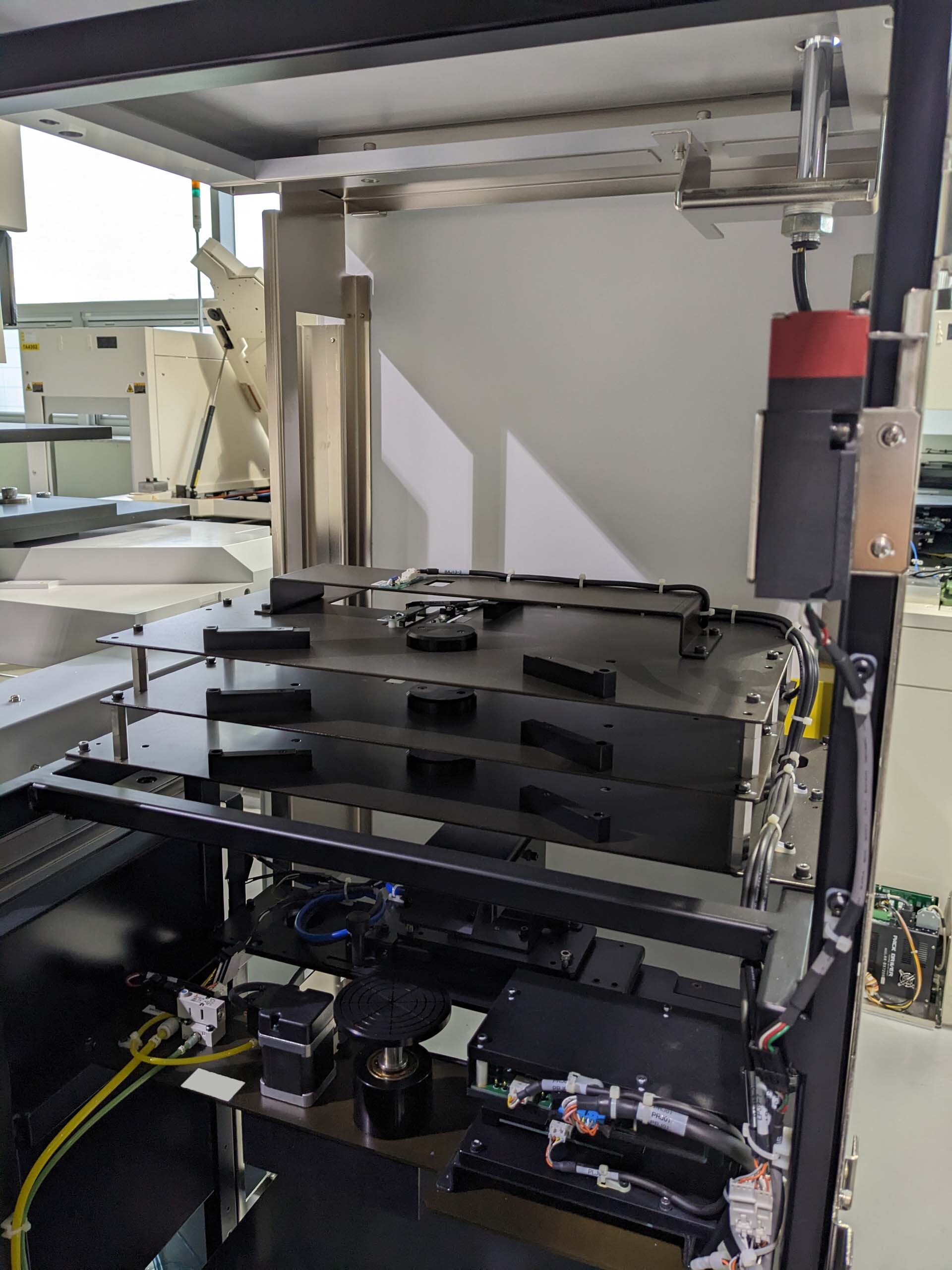
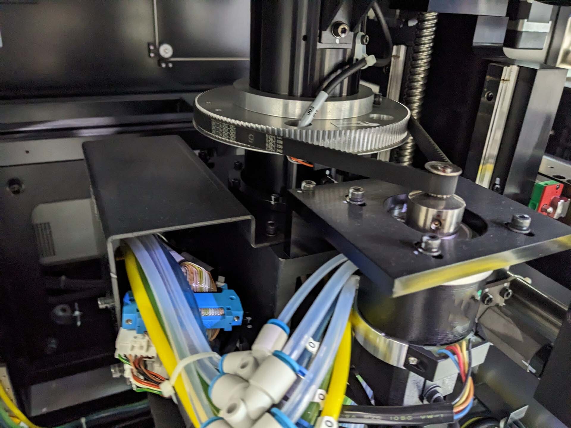
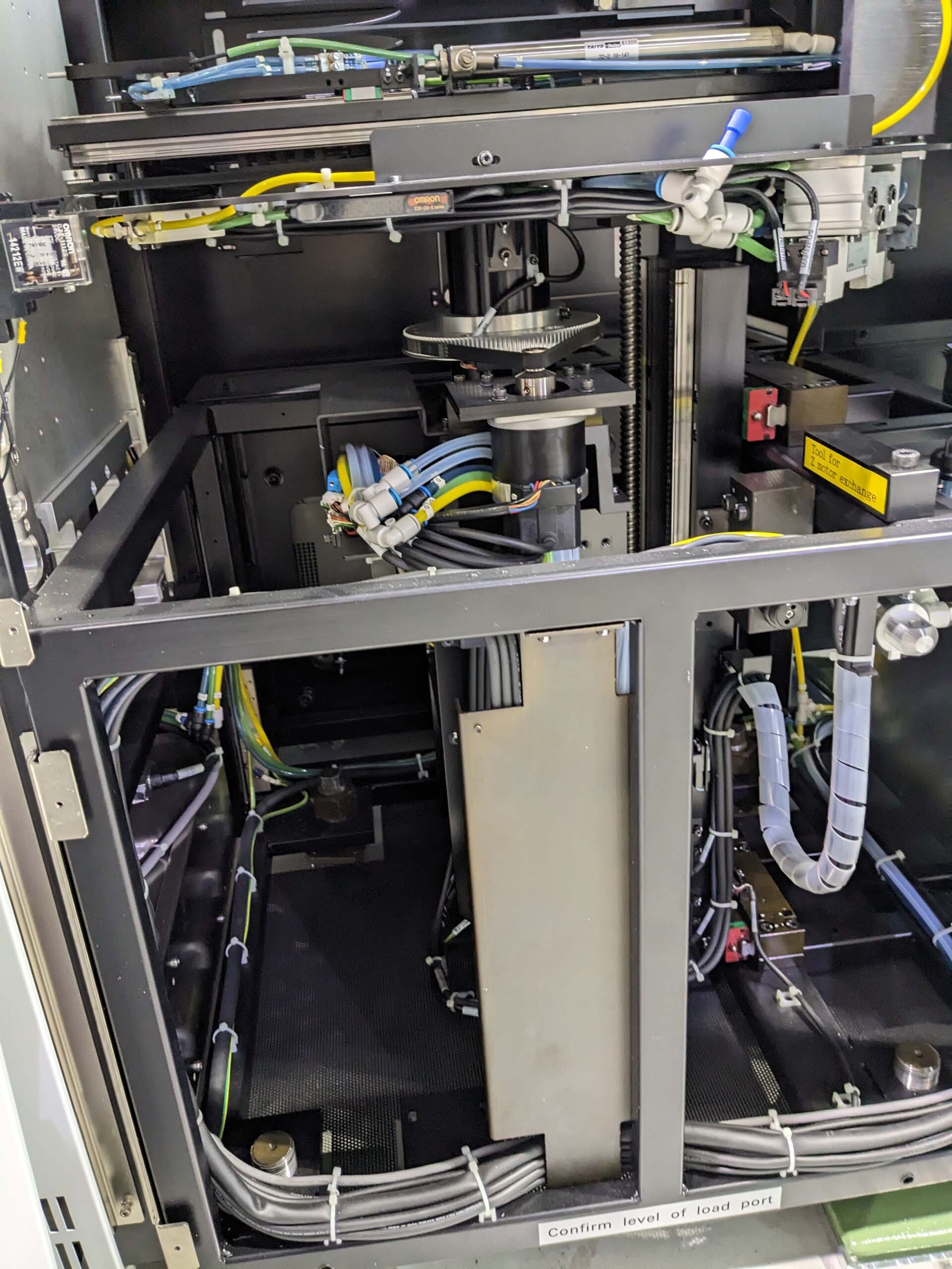
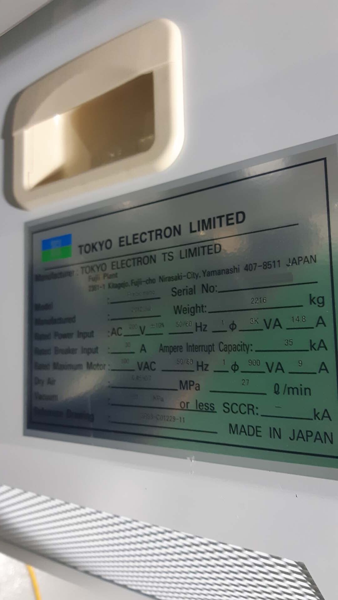
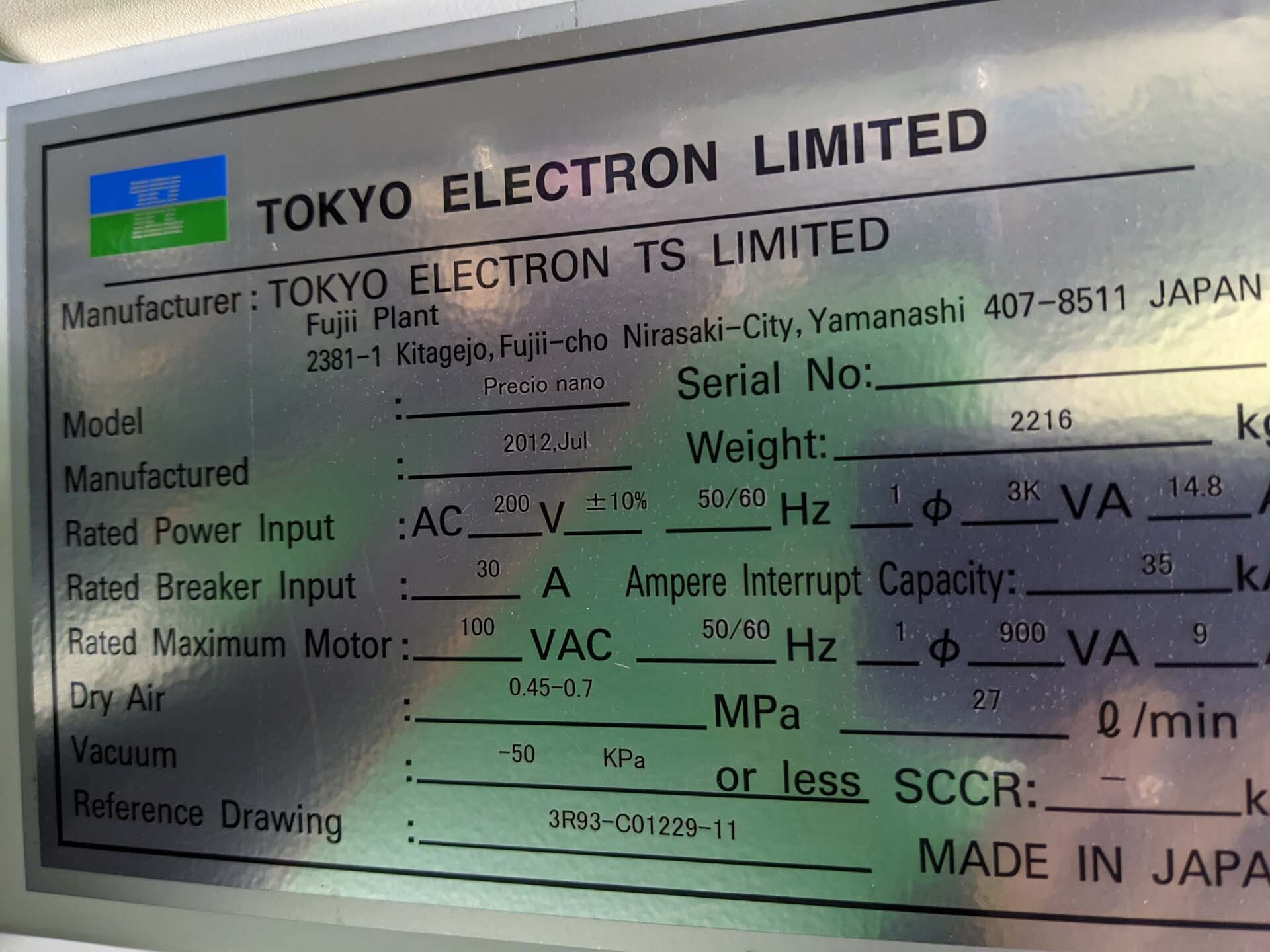
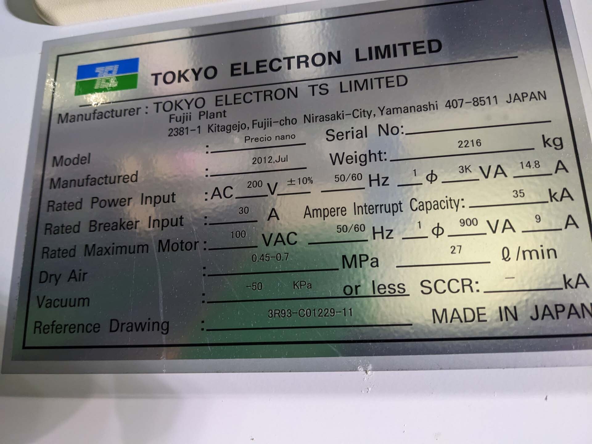
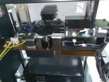
ID: 293663555
Wafer Size: 12"
Vintage: 2012
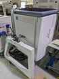
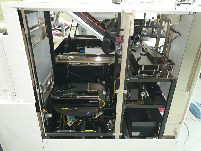
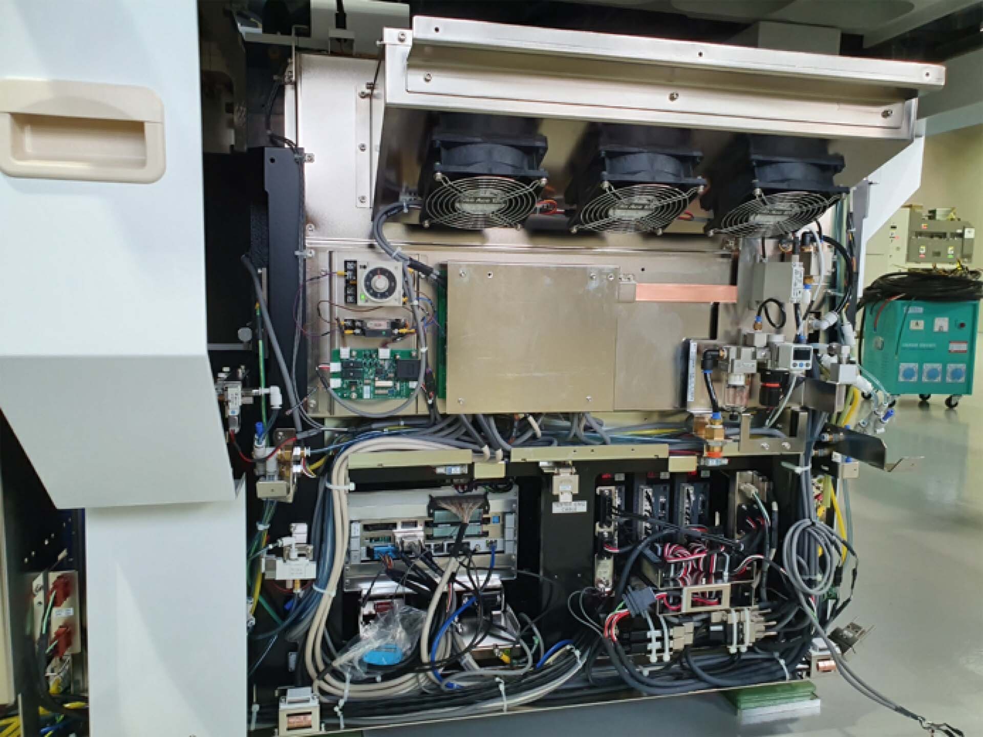
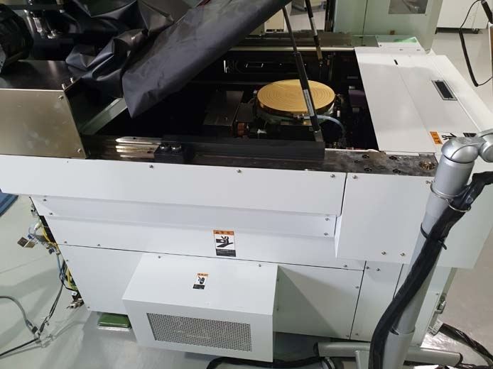
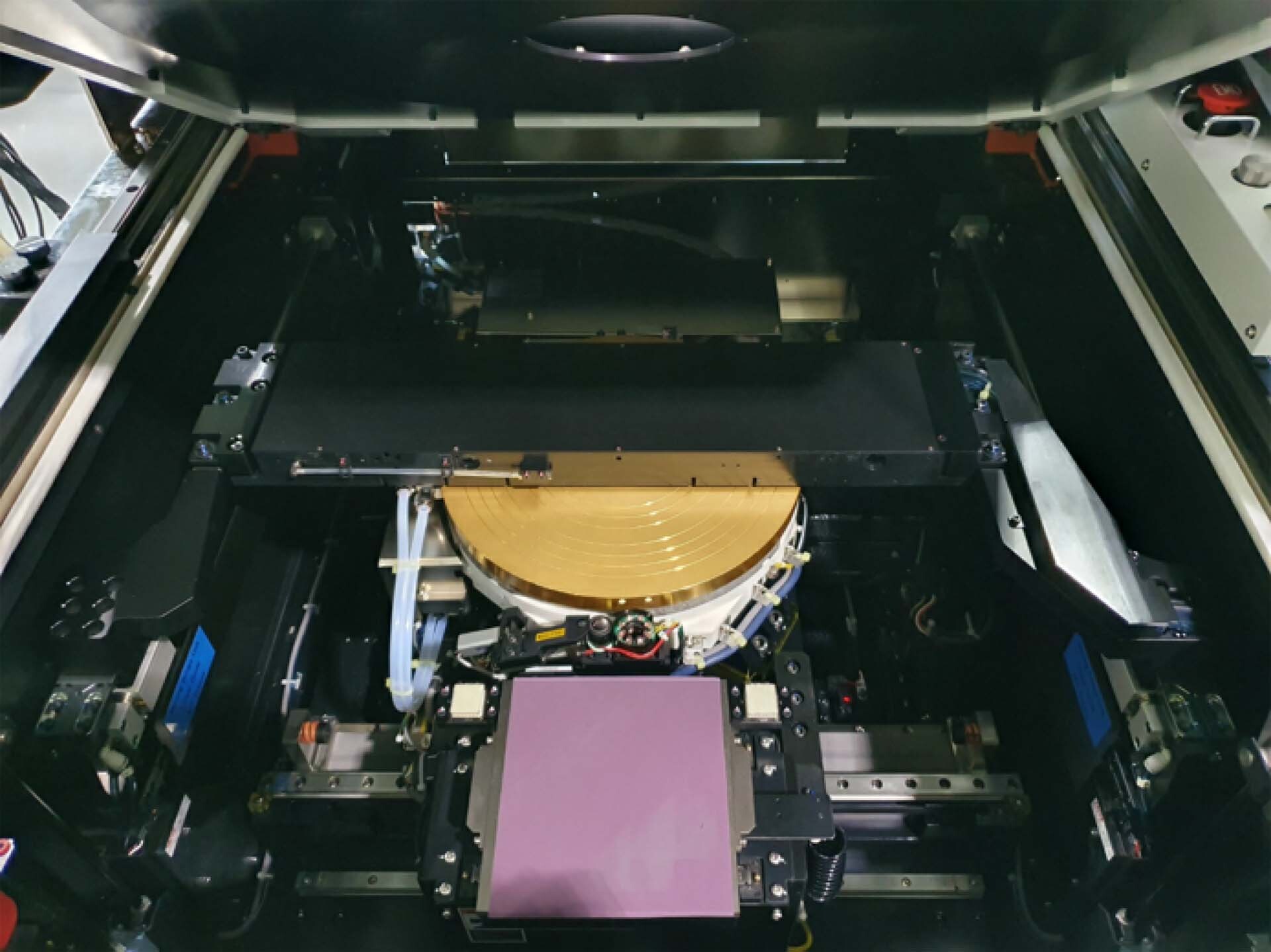
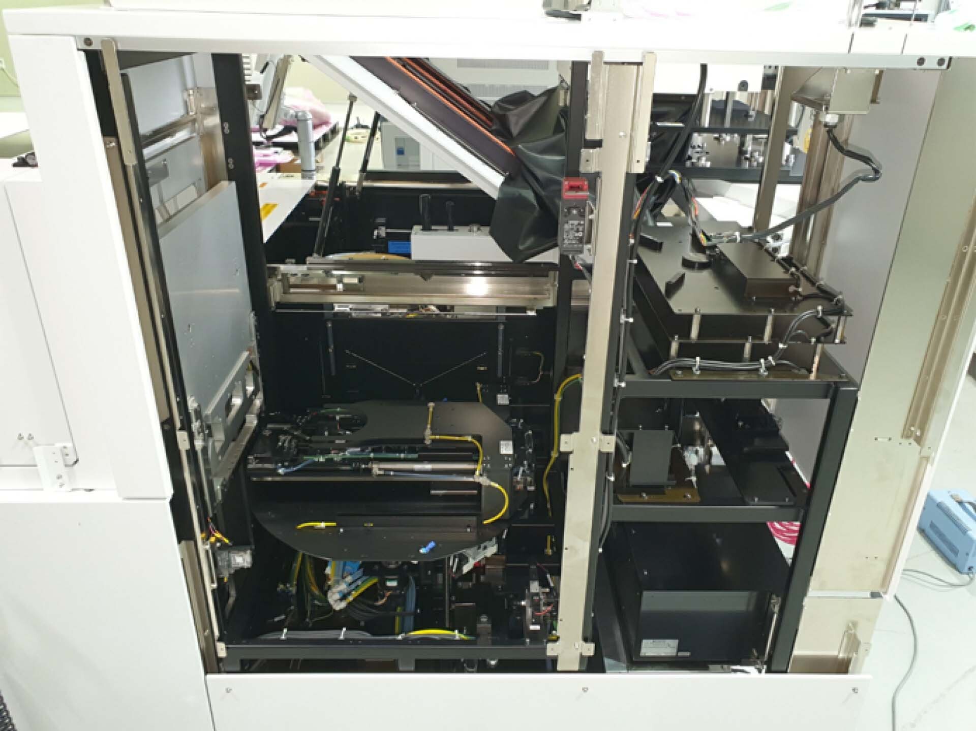
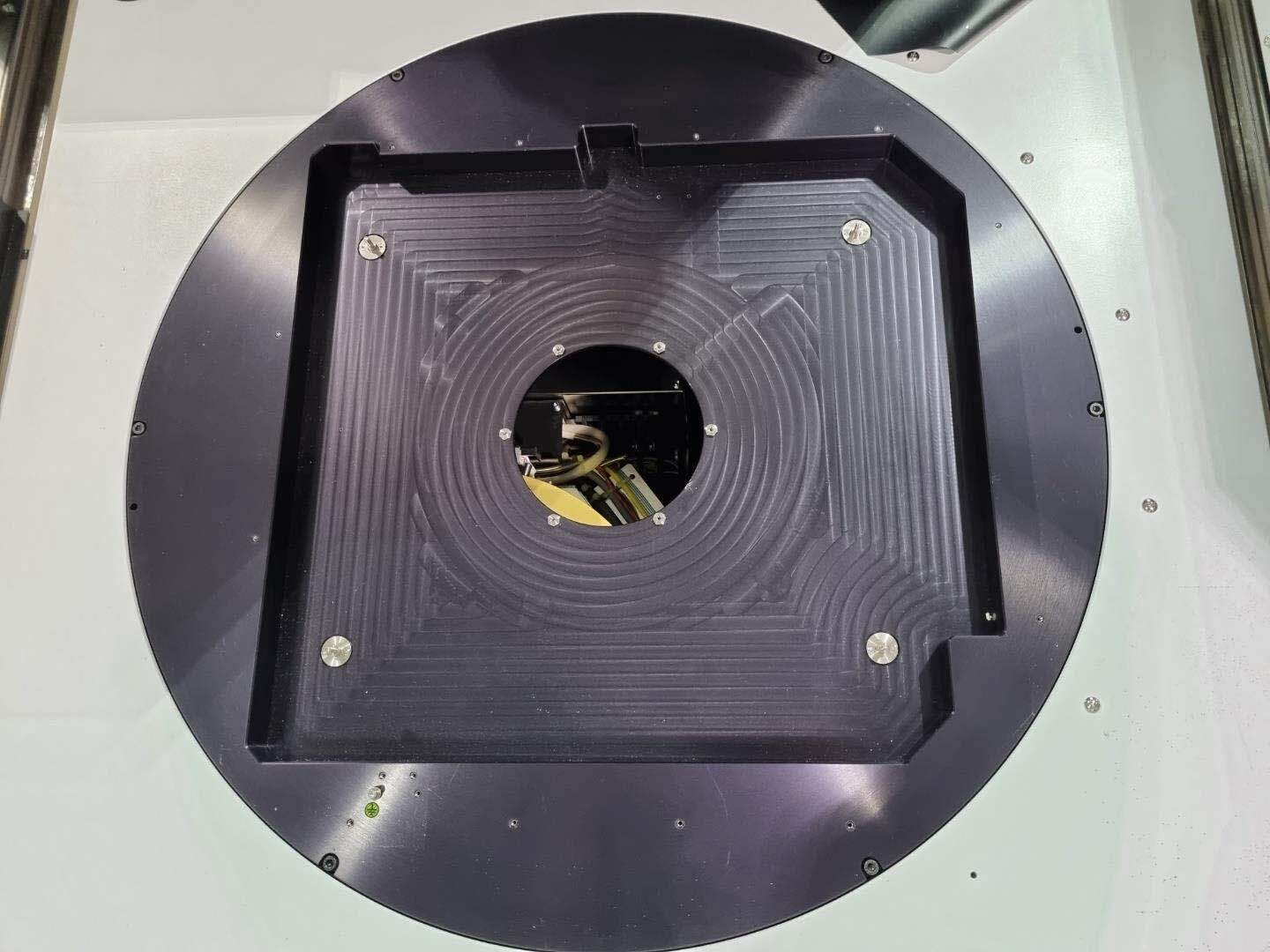
Wafer prober, 12"
Test temperature: Hot
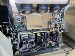
IP750EX Docked tester
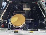
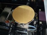
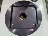
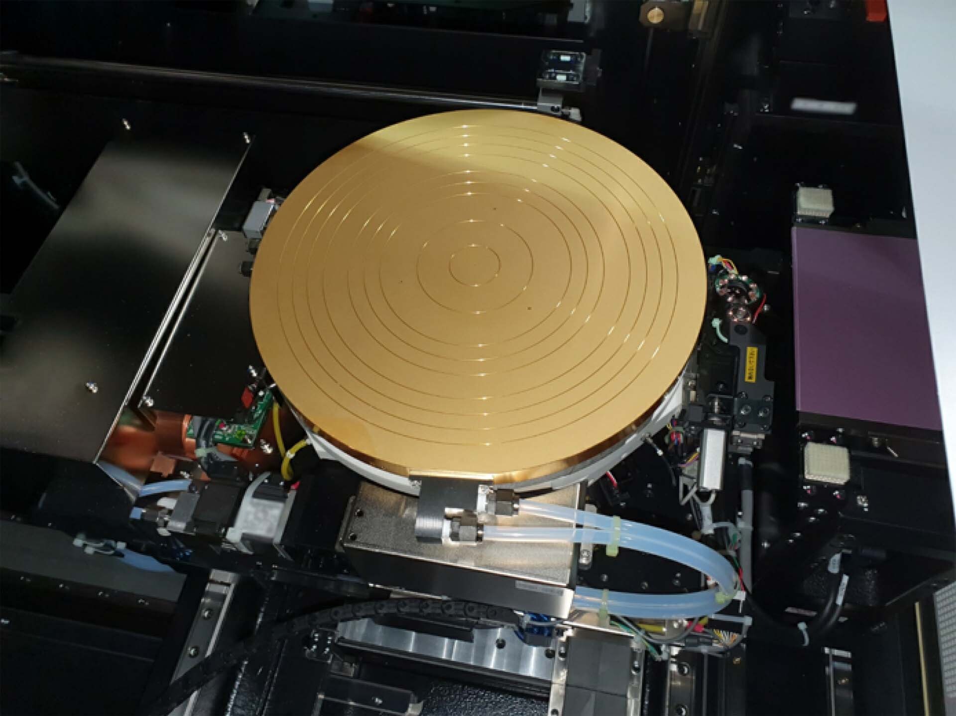
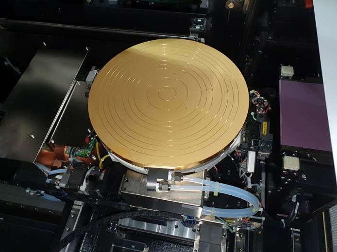
Chuck surface: Gold
Chuck type: Air-cool
Chuck temperature: 25°C to 150°C
CPU: DVE P7447/50
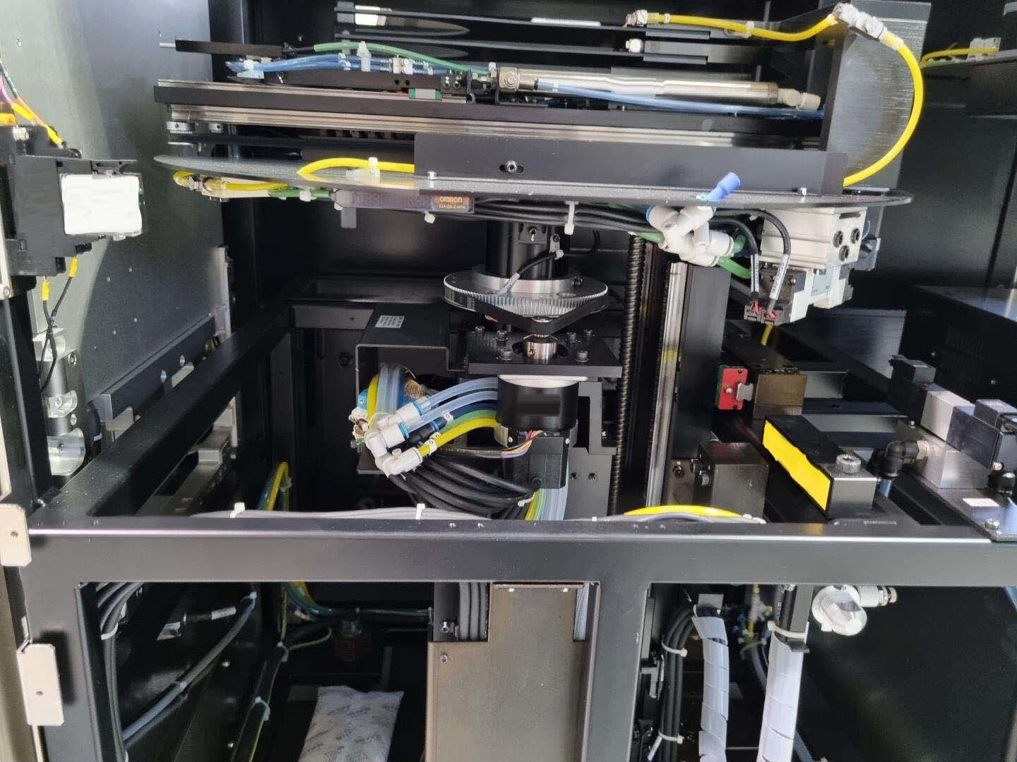
Right loader type: FOUP
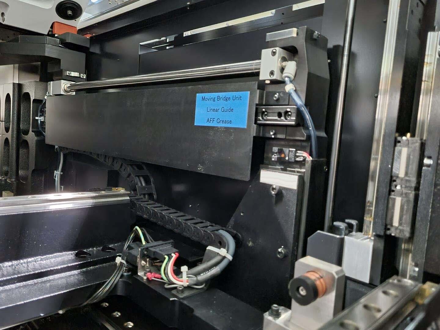
Bridge
GP-IB Cable
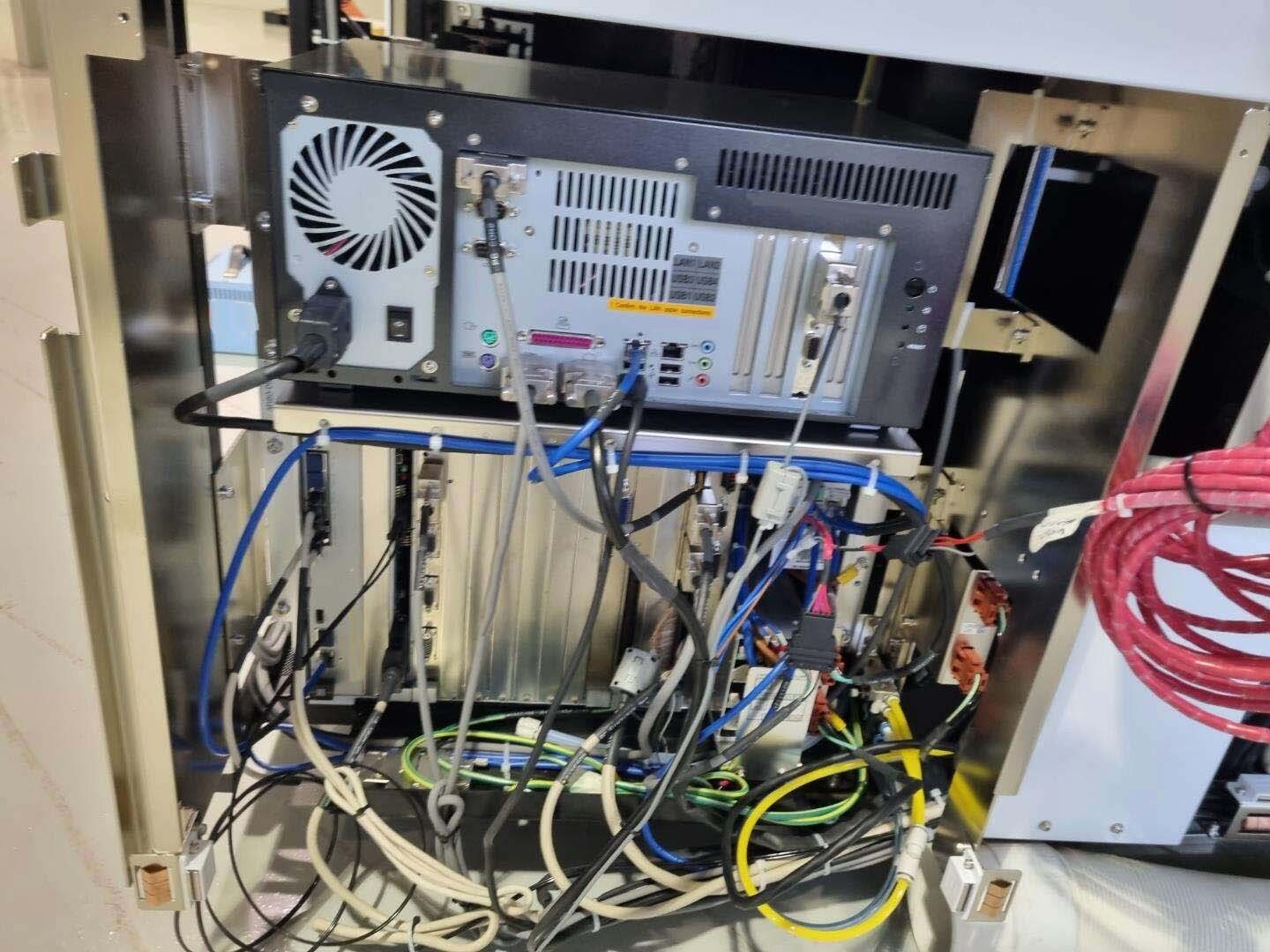
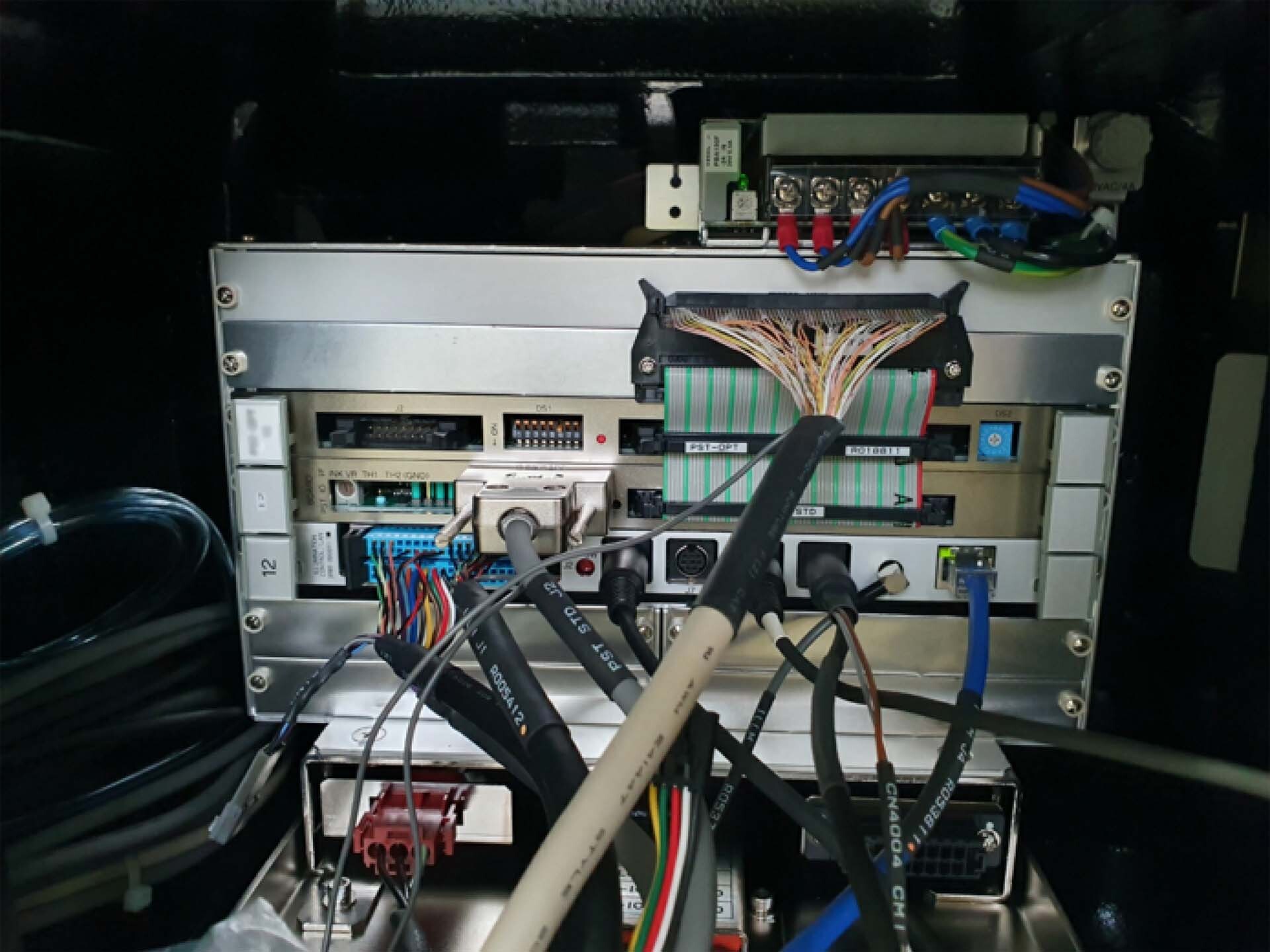
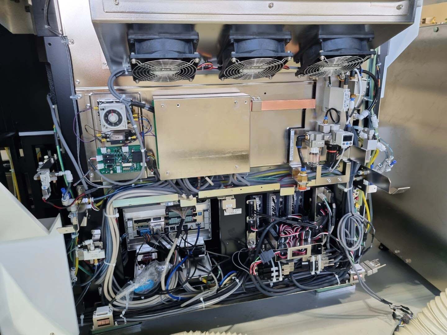
Controller
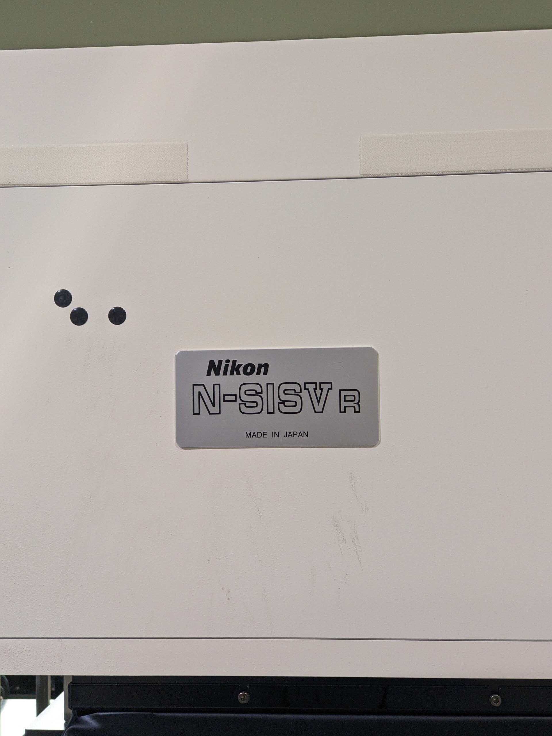
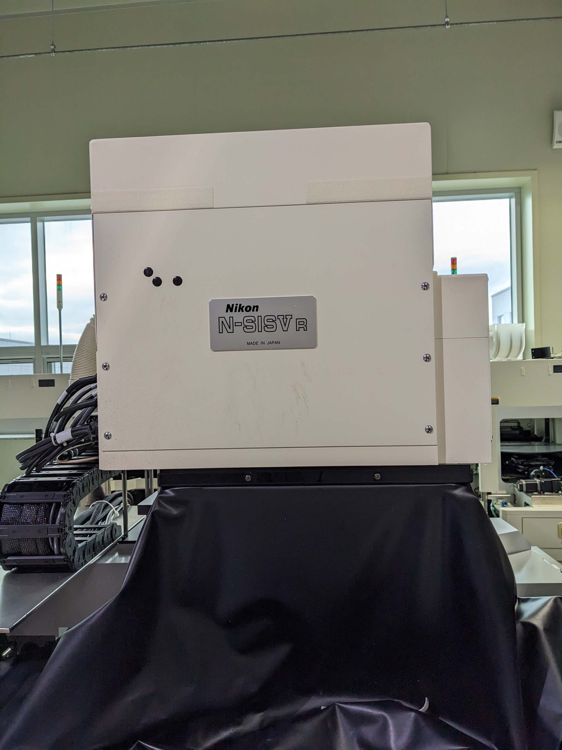
NIKON Illumination system
NIKON N-SISVR
No SACC
No hinge
No chiller
No printer
Options: OCR, FFU, WAPP
Power supply: 200 V
2012 vintage.
TEL / TOKYO ELECTRON Precio Nano is a leading supplier of semiconductor processing equipment and solutions, specializing in advanced technology for nanoscale semiconductor manufacturing. With a strong focus on innovation and cutting-edge research, TEL Precio Nano aims to provide customers with state-of-the-art tools for fabricating the most advanced semiconductor devices. The company's product portfolio includes a wide range of equipment and solutions for wafer processing, lithography, etching, deposition, cleaning, and metrology. These tools are designed to meet the demanding requirements of the semiconductor industry, including high precision, repeatability, and reliability. One of TOKYO ELECTRON Precio Nano's key offerings is its lithography equipment, which is essential for patterning the intricate features of semiconductor devices. The company's lithography tools utilize advanced technologies such as immersion lithography, multi-patterning, and extreme ultraviolet lithography (EUV) to achieve sub-10nm resolution and high throughput. In addition to lithography, Precio Nano also provides industry-leading etching equipment for shaping and defining the patterns created during the lithography process. The company's etching tools are capable of etching a wide range of materials with high selectivity and uniformity, ensuring the precise transfer of patterns onto the semiconductor wafer. Deposition is another critical process in semiconductor manufacturing, and TEL / TOKYO ELECTRON Precio Nano offers a comprehensive suite of deposition equipment for depositing thin films of materials onto the wafer surface. The company's deposition tools enable the formation of various film types, including dielectric films, metal films, and semiconductor films, with exceptional uniformity and conformality. Maintaining the cleanliness of semiconductor wafers is vital to ensure the quality and reliability of the final devices. TEL Precio Nano addresses this need with its advanced cleaning equipment, designed to remove contaminants and particles from the wafer surface without causing damage or defects. Metrology plays a crucial role in semiconductor manufacturing by providing accurate measurements of critical dimensions and parameters. TOKYO ELECTRON Precio Nano offers a range of metrology tools for inspecting and characterizing wafer features, enabling process control and optimization to achieve the desired device performance. Overall, Precio Nano stands out as a leading provider of semiconductor processing equipment and solutions, delivering advanced technologies and innovations to meet the evolving demands of the semiconductor industry. With a commitment to excellence and customer satisfaction, the company continues to drive technological advancement and push the boundaries of nanoscale semiconductor manufacturing.
There are no reviews yet