Used TEL / TOKYO ELECTRON Precio #293806769 for sale
URL successfully copied!
Tap to zoom
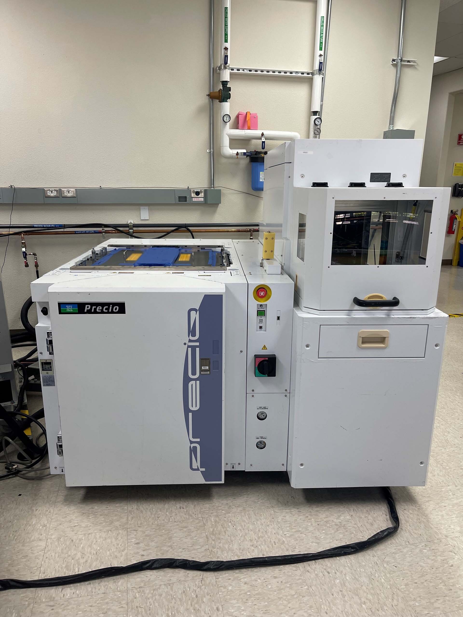

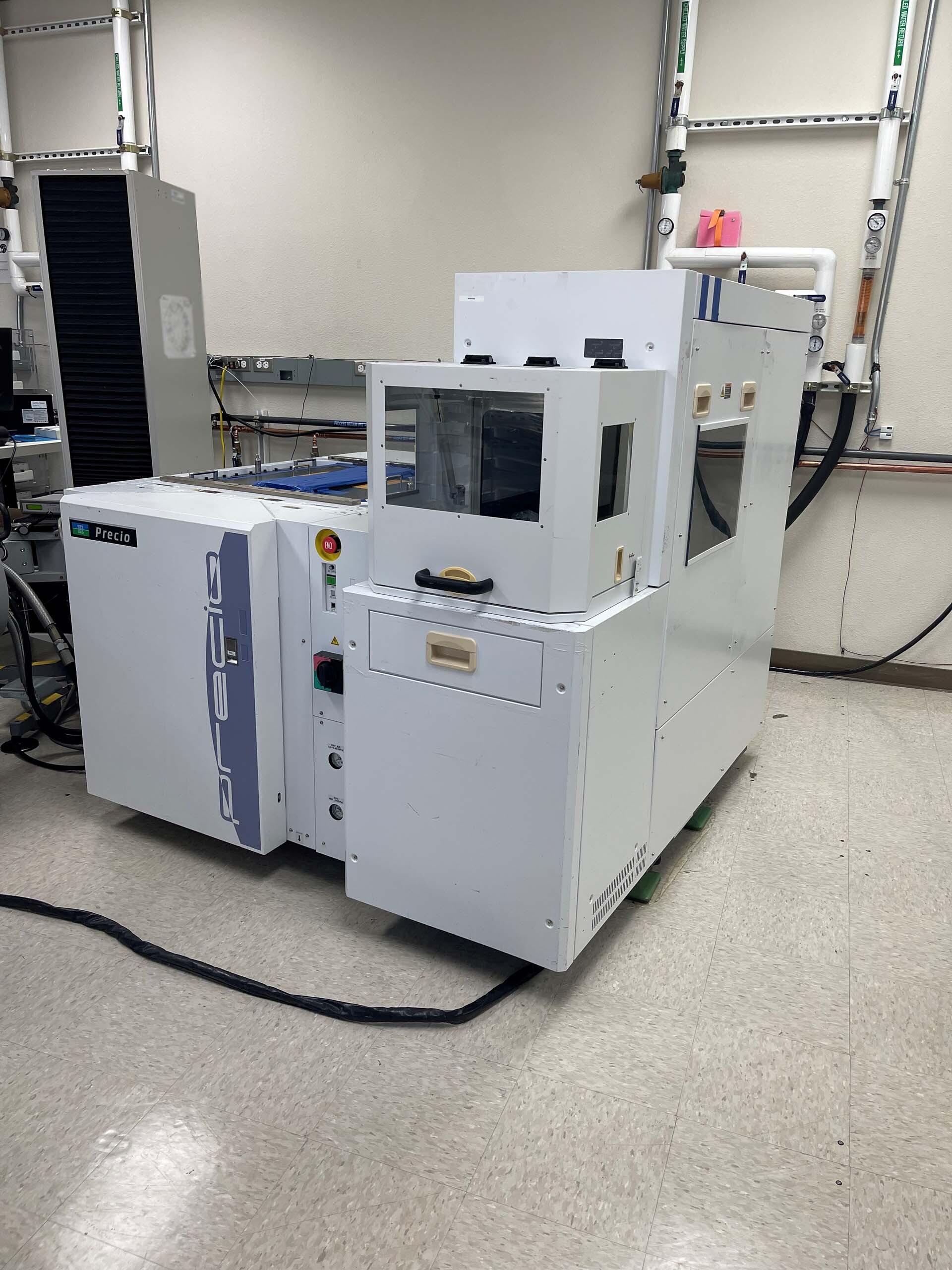
ID: 293806769
Wafer prober
Nickel plated chuck
Ambient temperature
480SQ Head plate
WAPP
Remote touch screen
Interface: GPIB
FOUP Loader, 12"
Cassette, 8".
TEL is a prober designed for wafer probing applications. It is a semi-automated probe station that facilitates accurate testing of wafers and other semiconductor components. The prober is designed with an XY movement stage, a high-precision Z-axis movement, and a high-speed scanning equipment to accommodate a multitude of wafer probing tasks. Additionally, the prober includes a low-vibration, three-axle-motor control system to ensure maximum accuracy during probing operations. The unit also offers a variety of features to support automated wafer probing and testing operations. It was designed with a combination of digital circuits and analog interface circuits to provide precise wafer probing and accurate wafer panel handling. This makes it able to operate with a wide variety of wafers, including standard, CNA (Corner Notch Alignments), non-standard sizes, as well as various non-flat substrates. The machine also allows for high-frequency operation up to four megabytes. This ensures that wafer testing and probing is conducted with the precision required to ensure the accuracy of the test results. The tool's user-friendly design enables users to setup a wide range of probe sequences for wafer probing. It also incorporates safety and monitoring functions to help prevent wafer damage. Furthermore, the prober comes with four replicating stages for sample staging. This provides users with flexible placement options for various wafer sizes and orientations. In addition, the asset includes an auto-match capabilities that enables users to quickly locate and identify a chip location in the wafer. This helps to ensure that the most accurate test result is obtained. The prober also features a flexible process environment with various options for data acquisition such as wafer alignment, misalignment compensation, signal integrity measurement, thermal data collection, etc. Additionally, this prober is certified to be compliant with EIA-JESD-228 testing requirements. This is a standard for testing products for electromagnetic compatibility. Overall, TOKYO ELECTRON prober is designed for wafer probing applications with an emphasis on accuracy and precision. It offers a variety of features to provide precise wafer probing and accurate wafer panel handling. The model also features a flexible process environment to accommodate various applications such as wafer alignment, misalignment compensation, signal integrity measurement, thermal data collection, etc. Furthermore, it is also certified to be compliant with EIA-JESD-228 testing requirements.
There are no reviews yet