Used TOKYO SEIMITSU A-PM-90A-N #293742994 for sale
URL successfully copied!
Tap to zoom
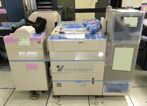

TOKYO SEIMITSU A-PM-90A-N is an advanced wafer prober system designed for high-precision semiconductor testing applications. This prober combines state-of-the-art technology with a user-friendly interface to deliver reliable and precise wafer probing performance. A-PM-90A-N is equipped with a range of features that make it suitable for both research and mass production environments. One of the key features of TOKYO SEIMITSU A-PM-90A-N prober is its high-speed and high-accuracy probing mechanism. The prober is equipped with advanced motion control systems that allow for precise positioning of the probe needles on the wafer surface. This ensures that the prober can accurately measure the electrical characteristics of the devices on the wafer with high repeatability. A-PM-90A-N prober is capable of probing wafers of various sizes, ranging from small semiconductor wafers to large glass substrates. The prober is equipped with motorized chuck tables that can accommodate different wafer sizes and shapes, making it versatile for a wide range of applications. The chuck tables are designed to securely hold the wafers in place during the probing process to prevent any misalignment or movement that could affect the accuracy of the measurements. In addition to its probing capabilities, TOKYO SEIMITSU A-PM-90A-N prober is also equipped with advanced alignment systems that ensure precise alignment between the probe needles and the devices on the wafer. The prober uses vision systems and alignment algorithms to automatically align the probes with the test pads on the wafer, reducing the need for manual alignment and increasing the overall throughput of the testing process. A-PM-90A-N prober also features a comprehensive software interface that allows users to easily set up test sequences, define probing parameters, and monitor the testing process in real-time. The software interface is intuitive and user-friendly, making it easy for both experienced and novice users to operate the prober efficiently. The prober is also compatible with industry-standard test automation software, allowing for seamless integration into existing testing workflows. Another key feature of TOKYO SEIMITSU A-PM-90A-N prober is its robust construction and high reliability. The prober is built with high-quality materials and components that are designed to withstand the rigors of semiconductor testing environments. The prober's components are carefully selected and tested for durability and longevity, ensuring that the prober can deliver consistent performance over an extended period of use. Overall, A-PM-90A-N prober is a versatile and reliable wafer probing system that offers high-precision testing capabilities for a wide range of semiconductor applications. Its advanced features, user-friendly interface, and robust construction make it an ideal choice for semiconductor manufacturers, research laboratories, and testing facilities looking to achieve accurate and reliable wafer probing results.
There are no reviews yet