Used KLA / TENCOR 2367 #9012614 for sale
It looks like this item has already been sold. Check similar products below or contact us and our experienced team will find it for you.
Tap to zoom


Sold
ID: 9012614
Wafer Size: 12"
Vintage: 2006
Brightfield inspection system, 12"
Install type: stand-alone
Cassette interface:
(2) Asyst 300mm FIMS LPs
(2) AdvanTag SW CID, G4
E84 for OHT with PIO for G4
E40/E94 HW support
Pre-aligner
Main unit:
Brooks robot
BB visible pixels (um): 0.62, 0.39, 0.25
BB/I-Line/G-Line UV pixels (um): 0.20, 0.16, 0.12
Edge contrast
Array and random modes
High mag review optics
High resolution review CCD
Anti-blooming TDI
IS station:
Status lamp (R, Y, G, B, Audible)
1600 MPSS image computer
Operating system: Windows 2000
Application SW ver: 10.4.507.0.5
GEM/SECS and HSMS
Power line conditioner
Remote power EPO
Facility requirements:
CDA
Vacuum (house)
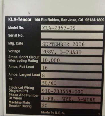
Power (main): 208 VAC, 16 A, 3 phase, 5 Wire (WYE), 50/60 Hz
Damaged / missing parts:
Assy, CC W backplane, CRTAESCAPE – COBRA, Part No. 0080512-000
Assy, PS2, 36/56VDC 91XX, 93XX, 2367 (exchange), Part No. 0281722-000
FRU, 2366, FPA-base (exchange), Part No. 0111806-000
Assy, FPA arm without A&C apertures, Part No. 0112397-001
Robot (exchange)
Robot controller (exchange)
Can be inspected
2006 vintage.
KLA / TENCOR 2367 Mask & Wafer Inspection equipment is a high-precision, automated wafer and photomask metrology and inspection system specifically designed for semiconductor manufacturing applications. The unit provides a fast, reliable solution for inspecting photomask and bare silicon wafer surfaces on production lines. KLA 2367 machine utilizes advanced inkjet technology to deposit an array of Ultraviolet (UV) fluorescent inspects on a photomask or wafer. These markers are then illuminated by a hyperspectral light source which generates a fringe pattern that is imaged by a complementary charge-coupled device (CCD) array camera.The fringe pattern is used to estimate the surface profile of the photomask or wafer and is compared against a user-defined specification. The tool then uses software algorithms to process and analyze the data to detect any surface anomalies or features. TENCOR 2367 Mask & Wafer Inspection asset has several benefits that help to improve the accuracy and productivity of semiconductor production. The model consists of multiple CCD cameras that are arranged to provide an optimal field of view coverage and depth of focus for mask pattern recognition. This ensures a higher accuracy of measurement. For wafer inspection, the equipment uses UV spectroscopy to detect wafer flatness, warp, pinspotting, and step height. The system is programmed to detect common flaws such as line breaks, gate bridging, and oxide nodules. Additionally, the optional automation option allows the unit to automatically match the positions of the wafers or masks relative to the light source for accurate inspection. 2367 Mask & Wafer Inspection machine is an advanced, productivity-enhancing solution that allows semiconductor manufacturers to reduce their overall inspection costs while ensuring quality control of their products. The tool's powerful software algorithms provide true 3D analysis of wafers and photomasks to provide highly accurate results. Additionally, it can be configured with an optional automation module to improve workflow and increase production throughput.
There are no reviews yet