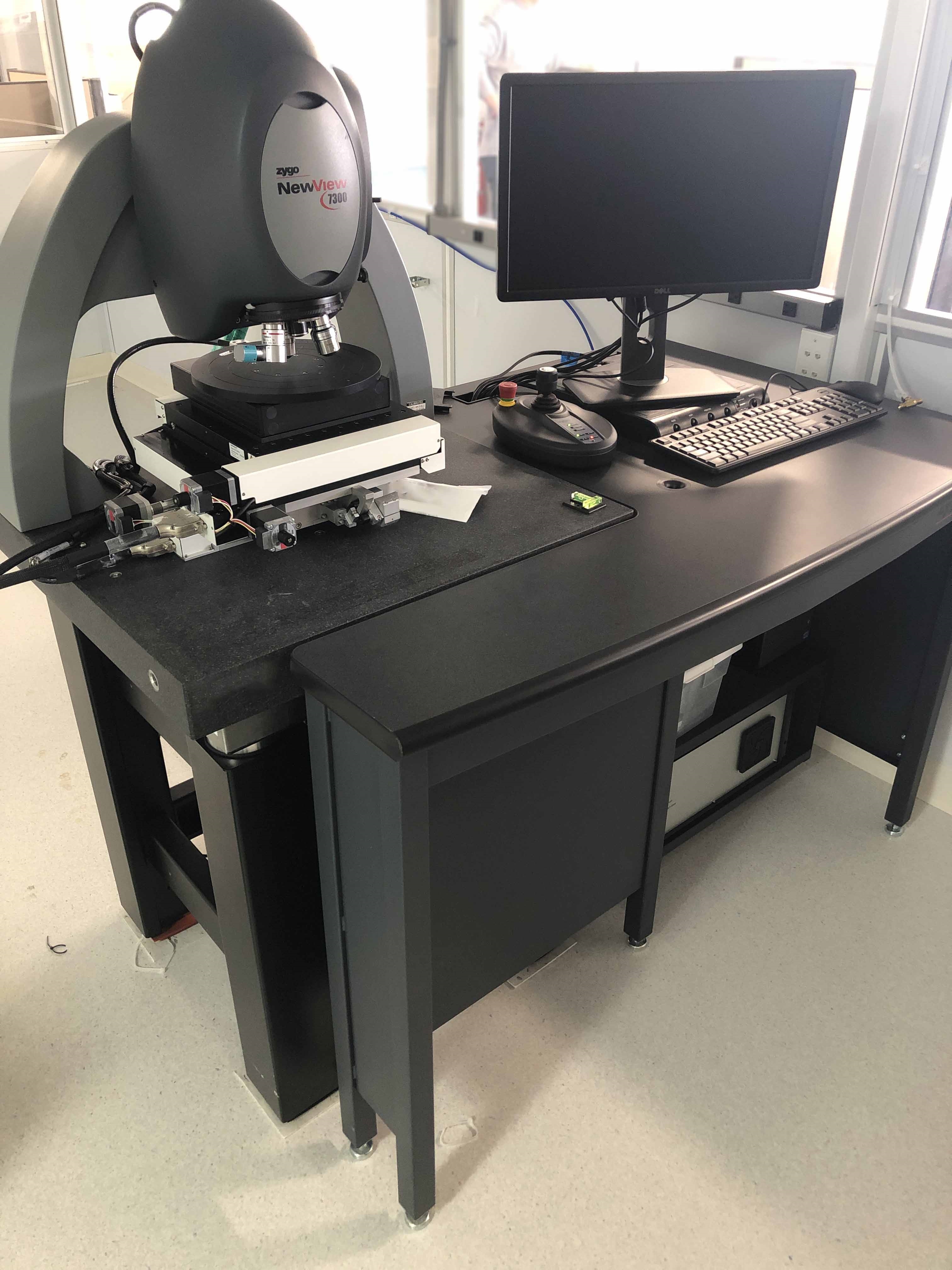
Used ZYGO NewView 7300 #9276460 for sale
It looks like this item has already been sold. Check similar products below or contact us and our experienced team will find it for you.
Tap to zoom


Sold
ID: 9276460
3D Optical profiling system
Stage, 8"
Mega pixel camera:
Automated 3-position multiple system
With 1.0x Zoom lens
Low noise
Large field
Digital closed loop piezo scanning
Transducer
Capacitive: 150 Micron scan
Illuminator with LED
Accommodates objectives: 1x - 100x
Extended scan, 20 mm
Vertical res: < 0.1 nm
RMS Repeatability: < 0.01 nm
Accessory:
6-Axis Base stage
Motorized Tip / tilt: X / Y / Z and theta included
Travel:
X / Y, 8"
Z, 4"
Rotation: +/- 90 Degree
PR travel: +/- 4 Degree
Options / Accessories:
Part number / Description
6300-0459-01 / Electronics, Power Kit 110/120 VAC (US) Included base system
6300-0650-02 / Manual encoded turret (4-Pos) (NV 600 / 700 / 6000 / 7000)
6300-0526-02 / Accessory: 2.0x Field zoom lens
6300-0522-02 / Accessory: 0.5x Field zoom lens
6300-0593-01 / Objective: 5x Michelson objective
6300-0595-01 / Objective: 20x AF Objective
6300-0597-01 / Objective: 50x Objective, thermally compensated
1840-700-105 / Vibration isolation table, 24 x 24 x 30 (LWH)
6300-2080-01 / Workstation table
6300-3434-01 / Workstation table, 1840-700-105 (NV 5000, 6000 and 7000 Series) / 1840-700-015 (GPI, MESA)
1776-666-012 / Accessory, SiC precision reference flat (30 mm Diameter)
1670-000-020 / Accessory, standard lateral calibration
1776-666-010 / Accessory, standard step height standard 1.75 um.
ZYGO NewView 7300 is a high-end mask and wafer inspection equipment developed to provide robust, dependable, and cost-effective solutions for mask makers and semiconductor manufacturers. It is a complete wafer and mask inspection system comprised of several state-of-the-art components. The unit features an advanced and precise optical subsystem for high-speed imaging of masks, silicon wafers, and flat panels. The optical configuration uses four bright, pulsed, one-millimeter-wavelength LEDs for expanded sensitivity and wide field of view. Additionally, the machine uses a specialized optical engine exclusive to ZYGO for maximum wafer coverage. ZYGO NEW VIEW 7300 also offers a 32-bit dual core processor with 512 MB RAM, enabling sub-micron resolution and speed for high-throughput screening and analysis of large die geometries. The tool utilizes a unique Real Image Capture with hybrid Chromatic Aberration Reduction (C.A.R.) technology for improved accuracy and resolution. Large, multi-vendor operation is supported by the included library of device and material parameter settings for optimal performance in production yields. The asset comes with a variety of analytical tools, including several imaging analysis, statistical analysis, multi-dimensional image dicing, and spectral yield analysis functions. The intuitive user interface provides powerful automation capabilities, allowing for detailed and rapid review of critical defects. It also supports large die-by-die inspections of defects, failure analysis, and process defect diagnostics and repair. NewView 7300 also offers several advanced capabilities for handling large wafers, and supports multiple chamber setup. The multi-layer mask inspection model can inspect up to 10 layers in a single pass, while the full-wafer inspection equipment can handle up to 25 layers in a single pass. The system utilizes a patented array of X, Y, Z prism stacks for homing and tracking, and for dimensional metrology of geometries. NEW VIEW 7300 is also compatible with several wafer handling subsystems, including automated wafer transfer and transport, multi-bay load ports, and sample prep systems. It can be integrated with a variety of third-party automation systems, allowing for the transfer and tracking of wafers without manual intervention. Finally, the unit is designed for easy maintenance, with a compact design and minimal spares requirements. In conclusion, ZYGO NewView 7300 is a powerful mask and wafer inspection machine designed to provide the fastest and most efficient way to monitor mask performance, wafer geometry, and feature dimensions. It offers advanced features, incredible accuracy, and flexibility for high-throughput screening and yield analysis.
There are no reviews yet