Used LAM RESEARCH / NOVELLUS PECVD System #293804484 for sale
URL successfully copied!
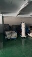
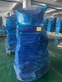

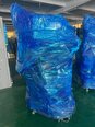
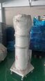
Tap to zoom
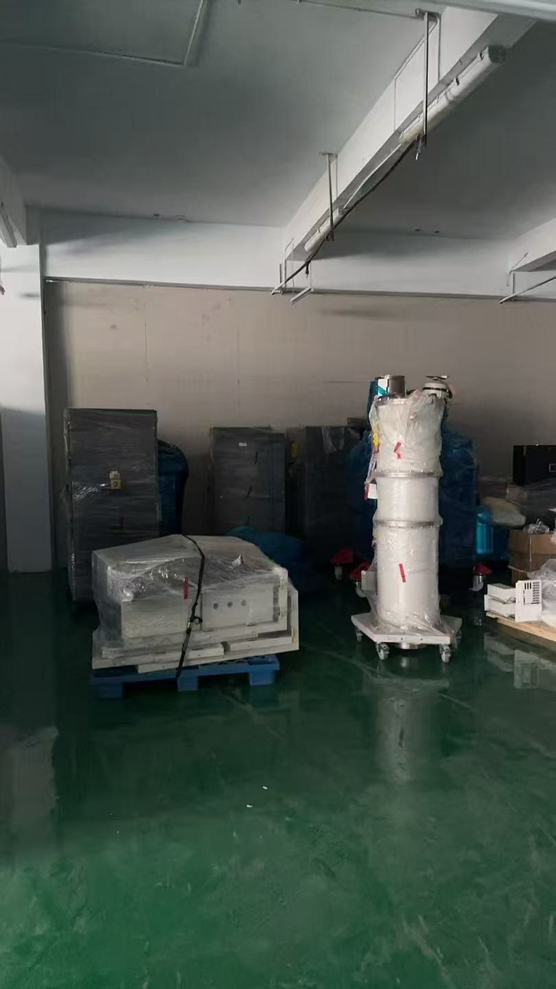

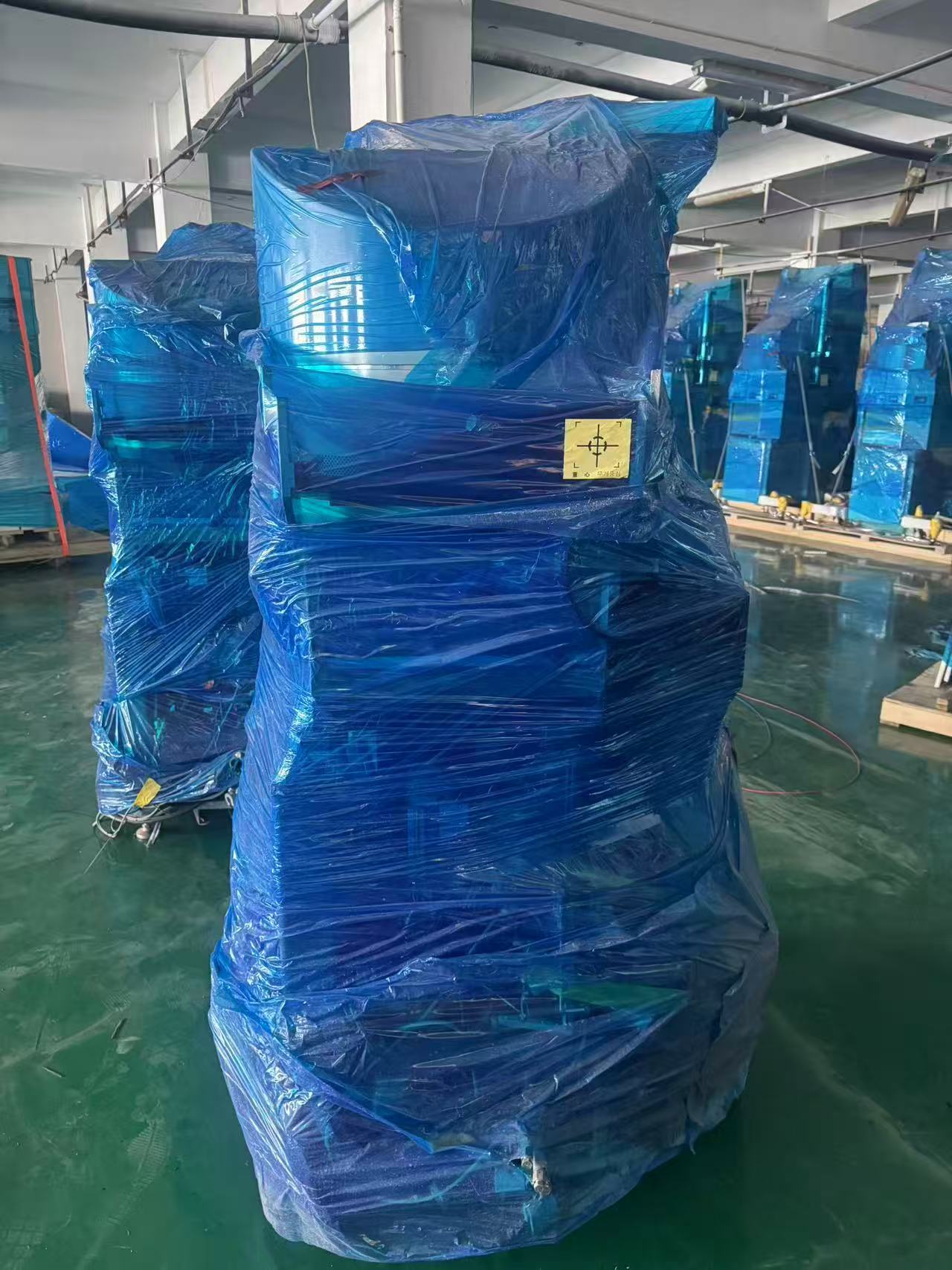
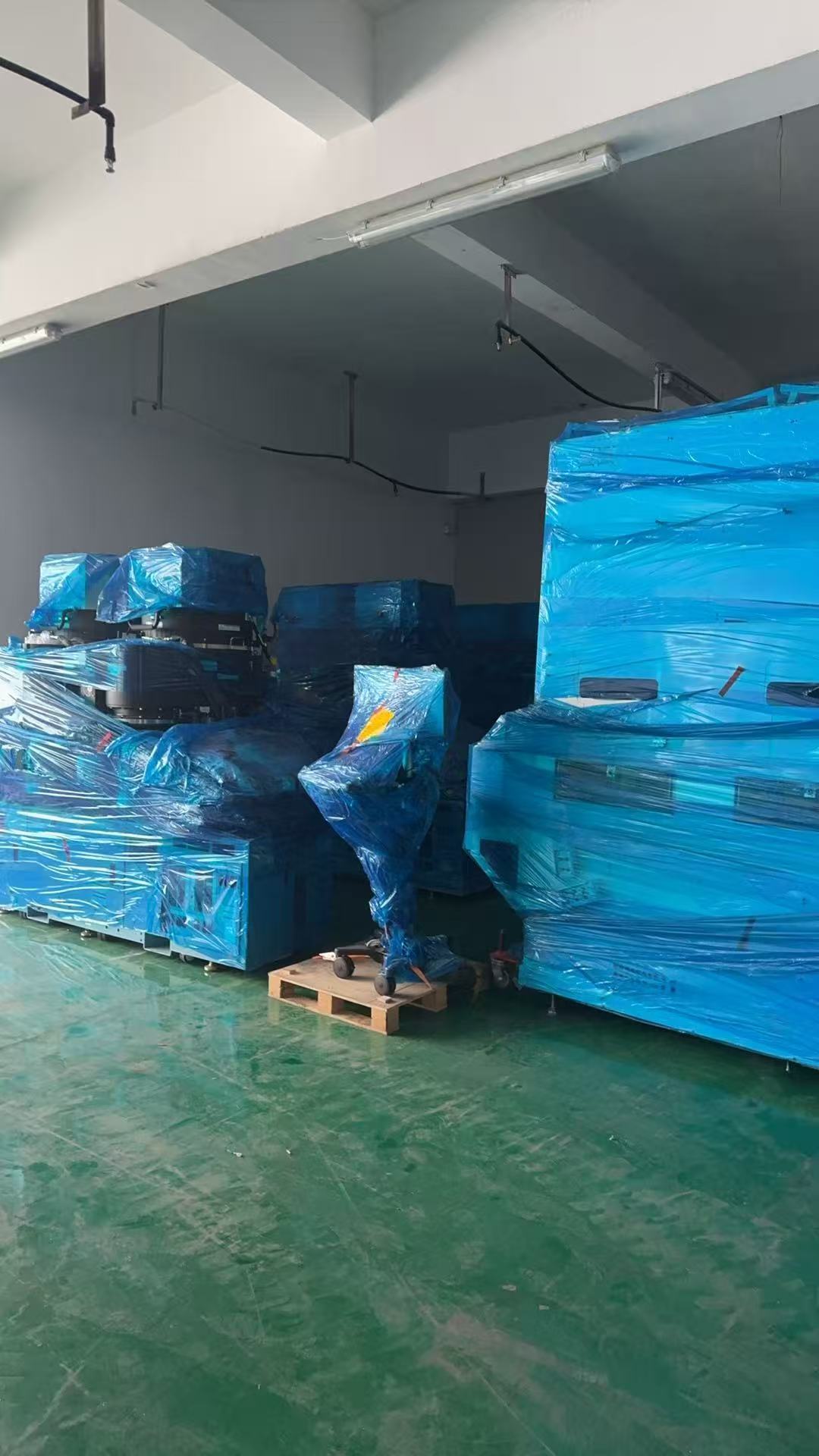
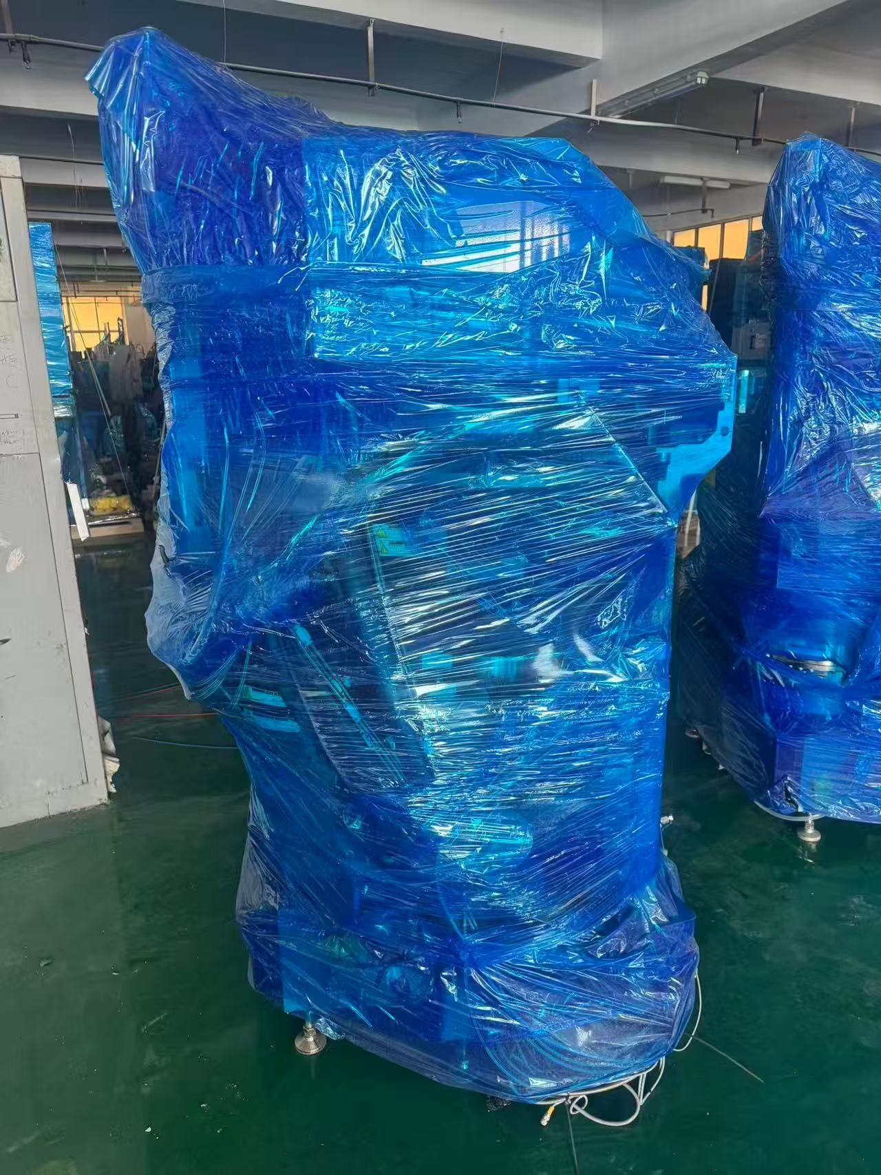
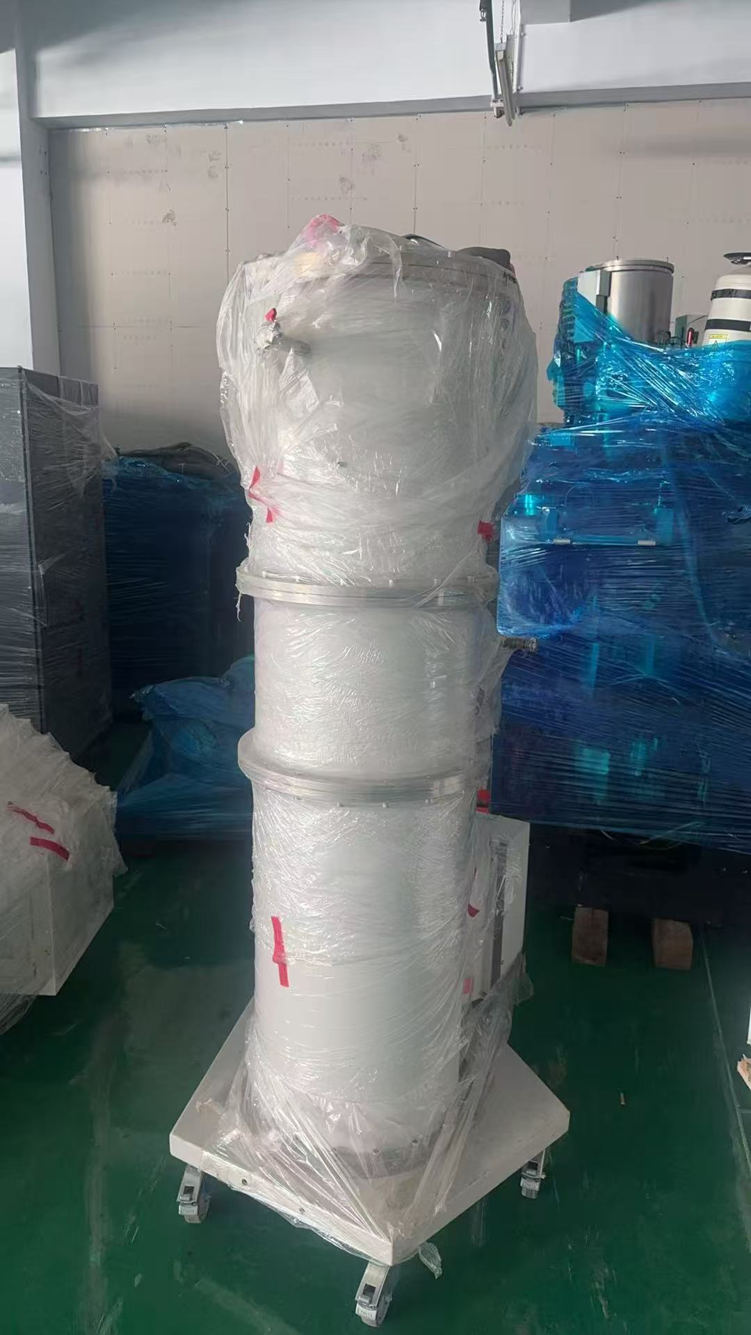
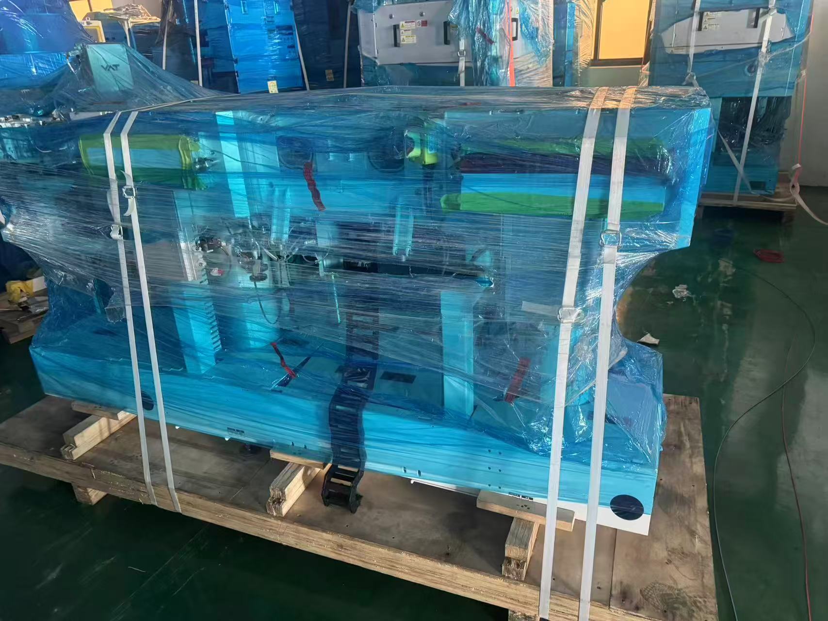
ID: 293804484
LAM RESEARCH / NOVELLUS PECVD Equipment Review NOVELLUS PECVD System is a state-of-the-art etcher/asher that offers advanced plasma-enhanced chemical vapor deposition (PECVD) capabilities for semiconductor manufacturing processes. Designed by the industry-leading semiconductor equipment manufacturer NOVELLUS in conjunction with LAM RESEARCH Systems, this unit provides a comprehensive solution for depositing thin film materials on silicon wafers with exceptional precision and uniformity. Key Features and Components LAM RESEARCH PECVD Machine is equipped with a range of cutting-edge features and components that enable high-performance PECVD processing. One of the key components of this tool is the plasma chamber, which houses the process gases and the plasma generation asset. The plasma chamber is designed to create a highly controlled plasma environment that facilitates the deposition of thin films on the wafer surface. The model also includes a gas delivery equipment that precisely controls the flow rates of the process gases into the plasma chamber, allowing for the accurate deposition of various thin film materials. Additionally, PECVD System features a temperature control unit that maintains the wafer at the desired temperature during the deposition process, ensuring optimal film quality and uniformity. Process Control and Monitoring LAM RESEARCH / NOVELLUS PECVD Machine is equipped with advanced process control and monitoring capabilities that enable real-time optimization of the deposition process. The tool features a comprehensive software interface that allows operators to program and control all aspects of the deposition process, including gas flow rates, temperature profiles, and deposition parameters. Moreover, the asset includes in-situ monitoring tools that provide real-time feedback on the film thickness, uniformity, and quality during deposition. This allows operators to make immediate adjustments to the process parameters, ensuring consistent film properties across the entire wafer surface. Wafer Handling and Automation NOVELLUS PECVD Model is designed for high-throughput semiconductor manufacturing applications and features advanced wafer handling and automation capabilities. The equipment includes a robotic wafer handling system that can automatically load and unload wafers from the process chamber, minimizing operator intervention and reducing the risk of wafer contamination. Furthermore, the unit is equipped with a wafer mapping machine that identifies the location of each individual wafer on the process chuck, allowing for precise control over the deposition process on a wafer-by-wafer basis. This ensures consistent film properties and quality across a batch of wafers, maximizing yield and productivity in semiconductor production. Applications and Benefits LAM RESEARCH PECVD Tool is widely used in the semiconductor industry for a variety of applications, including the deposition of dielectric films, passivation layers, and anti-reflective coatings on silicon wafers. The asset offers several key benefits, including high deposition rates, excellent film uniformity, and superior film quality, making it an ideal solution for advanced semiconductor fabrication processes. Overall, PECVD Model is a cutting-edge etcher/asher that provides semiconductor manufacturers with a reliable and efficient solution for depositing thin film materials on silicon wafers. With its advanced features, process control capabilities, and automation functionality, this equipment is well-suited for a wide range of semiconductor manufacturing applications, driving innovation and productivity in the industry.
There are no reviews yet