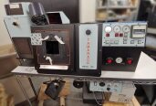
Used Mask Generation & Production for sale
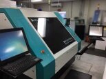
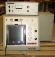
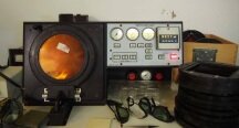
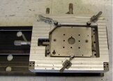
Mask generation production is a crucial process in semiconductor manufacturing that involves the creation of photomasks used for lithography. Photomasks are high-precision optical plates that contain the patterns of integrated circuits (ICs). These patterns are then transferred onto silicon wafers during the lithography process. The first step in mask generation production is designing the IC layout using computer-aided design (CAD) software. The design includes the circuit components, interconnects, and other elements specific to the IC's function. Once the layout is finalized, it is converted into a series of binary data points representing the patterns. Next, the binary data is used to generate the photomask patterns. This involves a series of highly advanced processes, including electron beam lithography or optical projection. Electron beam lithography uses a focused electron beam to directly write the patterns onto the mask, while optical projection utilizes a complex system of lenses to transfer the patterns onto the mask using light. After the mask patterns are generated, they undergo rigorous quality control checks. This includes inspecting for defects, verifying pattern alignment, and ensuring accurate dimensions. Any imperfections or errors are corrected before moving on to the next step. Finally, the finished photomask is ready for use in the semiconductor manufacturing process. It is then used during lithography to transfer the patterns onto the silicon wafer, forming the intricate circuitry of the IC. In summary, mask generation production is a highly technical and precise process involving the design, creation, and quality control of photomasks used in semiconductor manufacturing. It is a critical step in the production of integrated circuits and plays a vital role in ensuring the functionality and performance of electronic devices.
Filters
-
(3)
-
(2)
-
(2)
-
(4)
-
(1)
-
(1)
-
(2)
-
(3)
-
(4)
-
(8)
-
(3)
-
(3)
-
(3)
-
(1)
-
(2)
-
(1)
-
(1)
-
(1)
-
(1)
-
(1)
-
(17)


