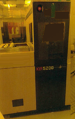
Used KLA / TENCOR 5200XP #9118489 for sale
It looks like this item has already been sold. Check similar products below or contact us and our experienced team will find it for you.
Tap to zoom


Sold
ID: 9118489
Wafer Size: 8"
Vintage: 1997
Overlay measurement system, 8"
Hardware:
Chuck 8"
Autoloader
(2) 8" open cassette load ports
Main VME card cage
Motor VME card cage
Flotation module
LINNIK and KLAASP
Power module
Hardware configuration:
Main console
Handler: dual open cassette
(2) Load ports: 8" open cassette
Signal tower
GEM/SECS
Network
Standard wafers: DSW75.1
Main VME card cage:
CPU board
Memory board
Video (frame grabber) board
I/O board
PZT controller board
Motor VME card cage:
Motor CPU board
Stepper driver board 1-4
Encoder interface board
Stage:
XYT stage
Z Motor
Host chuck
Z PZT
X PZT
Y PZT
PM target
Floatation module:
(4) Isolators
(3) Proximity sensors
PID board
LINNIK and KLAASP:
Arc lamp housing
Dual aperture
LLG
LINNIK camera
PIN diode array
P PZT
Shutter
KLAASP camera
Power module:
Power transformer
AC compartment
Main DC power supply
Arc lamp power supply
Vacuum and pressure air inlet
(3) Vacuums
CDA
Software:
Windows NT 4.0
Software 14.60.02
GEM/SECS
KLASS 4.1.1.1
Computer configurations:
Pentium II 400 MHz CPU
128M Ram
(2) 9G hard drive disk
Floppy drive
CD ROM
Tape driver
Monitor
Thermal printer
Keyboard/track ball
Options: UPS
Facilities:
225VAC, 50/60 Hz input power
25"Hg input vacuum
97-110 PSI input CDA
Manual
1997 vintage.
KLA / TENCOR 5200XP is a state-of-the-art wafer testing and metrology equipment designed for increased performance and reliability. It is essential to the development and production of semiconductor devices and a wide range of materials and substrates, such as silicon, gallium arsenide and thin films. KLA 5200XP has a unique patented design architecture that includes a multi-slice macroscopic imaging system, a powerful image acquisition and image processing unit, an advanced interferometry machine, and a fully customizable metrology software. This tool has high-resolution imaging support and measurement capabilities, which include automatic sample topography plotting and overlay mapping. It utilizes a two-dimensional defect detection algorithm with high pixel resolution and a 16-bit signal-to-noise ratio and a 4-megapixel CCD camera. Wavefront aberration and Zernike decomposition are also included, to measure factors such as surface roughness, flatness, power, radius of curvature, defocus, astigmatism, and tilt. All parameters are easily set via a user-friendly touchscreen interface. TENCOR 5200 XP is designed with an expandable internal memory, and it can store up to 30,000 images. The device supports both data streaming to an external computer and stand-alone operation. It also features an autofocus asset with advanced auto-zoom, pan, and tilt modes, to optimize sample viewing with minimum effort, and the unit is capable of measuring sample sizes up to 10 inches in diameter. Installation, cleaning and maintenance are easy, due to the variable-sized robotic sample tray, and the model includes up to mid-level dry pumping for high-contamination environments. In addition, 5200XP wafer testing and metrology equipment has standard IEEE communications, as well as a range of other options, such as wireless connectivity, data link security and remote, online diagnostics. KLA / TENCOR 5200 XP is the ideal choice for a wide range of wafer testing and metrology applications including mobile device IC characterisation, failure analysis, process troubleshooting, and yield analysis. It provides faster than ever performance and highly accurate results, with an unparalleled level of reliability, helping to reduce costs and increase device yields.
There are no reviews yet