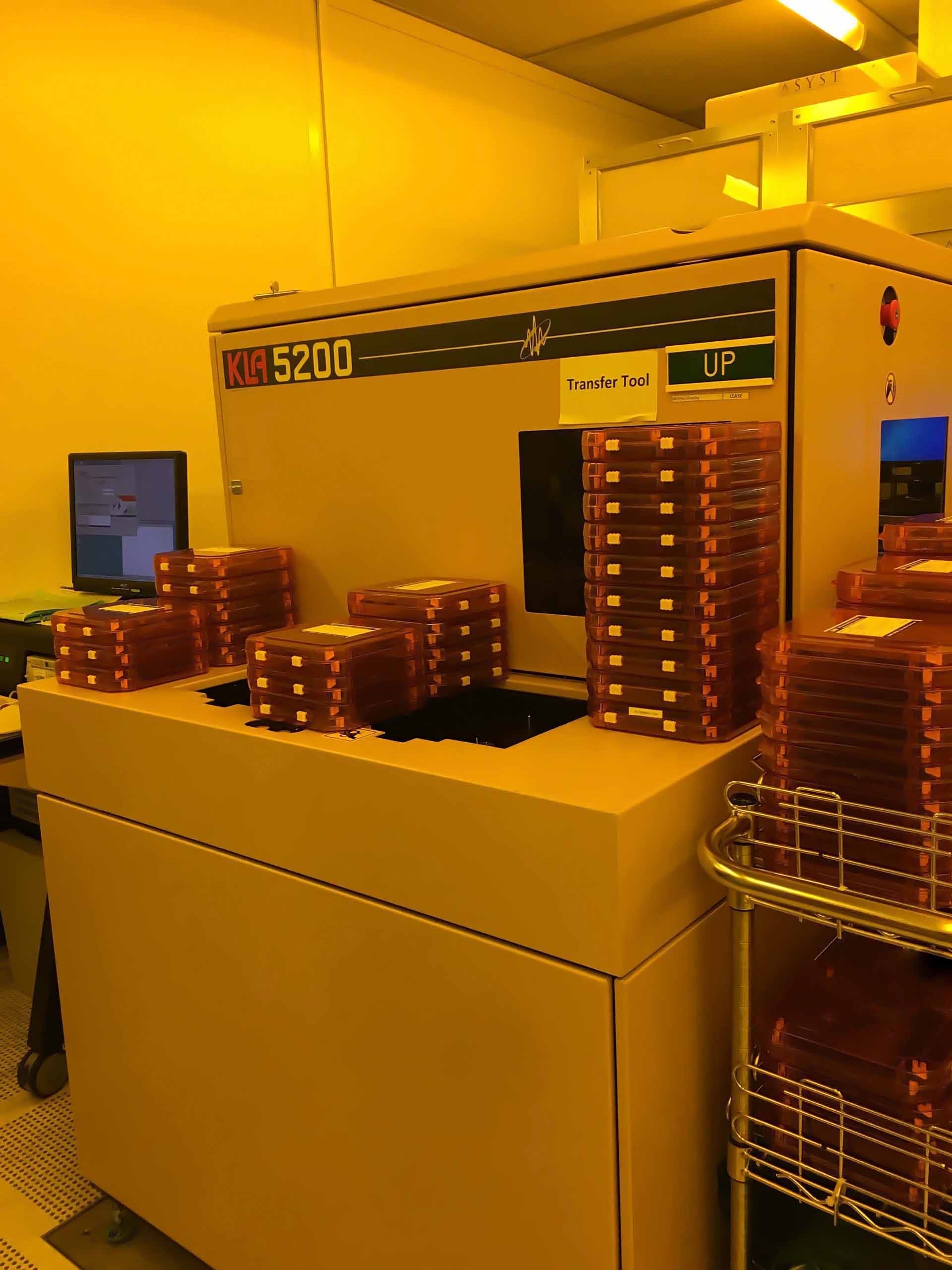
Used KLA / TENCOR 5200XP #9214648 for sale
It looks like this item has already been sold. Check similar products below or contact us and our experienced team will find it for you.
Tap to zoom


Sold
KLA / TENCOR 5200XP is a wafer testing and metrology equipment designed for both metrology and inspection applications in semiconductor production. Capable of both high-accuracy and high-throughput solutions, KLA 5200XP system can be used to increase yield and reliability. This unit utilizes advanced imaging technology, such as time-of-flight secondary electrons and backscattered electrons, which allows it to provide superior resolution imaging and high-sensitivity defect detection. Additionally, deconvolution algorithms provide the ability to identify smaller features and defects. Automated alignment and imaging features such as step and scan and image stitching allow the machine to reduce the total area it needs to image, while requiring fewer user interactions. TENCOR 5200 XP also includes various features that enhance image analysis, such as automated defect classification algorithms and a library of reference designs to allow users to accurately compare results to known standards. Furthermore, through its interfacing with other systems such as optical inspection systems and first-level defect analysis systems, KLA 5200 XP provides a more integrated and efficient workflow for defect analysis. The tool can additionally provide metrology solutions for a variety of applications, including measurements for critical dimension, CD uniformity, overlay accuracy, and line flatness. It also integrates laser interferometry, which can be used to measure the dramatic changes in feature critical dimension and layer height caused by process variations. KLA / TENCOR 5200 XP also has multiple stage automation, enabling the asset to move from wafer to wafer with high precision and accuracy. 5200XP has become the go-to metrology and inspection model for a variety of applications, thanks to its combination of superior resolution imaging, advanced defect detection algorithms, and automation capabilities. Its ability to interface with other systems ensures an efficient, integrated workflow that improves the overall yield and reliability of wafers.
There are no reviews yet