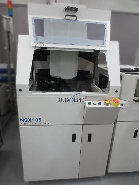
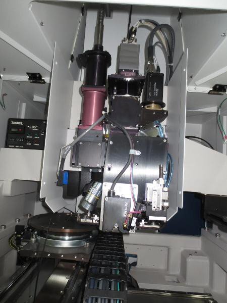
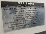
Used RUDOLPH / AUGUST NSX 105C #9273802 for sale
URL successfully copied!
Tap to zoom


ID: 9273802
Wafer Size: 8"
Vintage: 2007
Inspection system, 8"
BROOKS (Robot and aligner)
Type C
(2) Load ports
2007 vintage.
RUDOLPH / AUGUST NSX 105C is an advanced mask and wafer inspection equipment for semiconductor manufacturing environments. It combines optical and x-ray imaging, automated critical dimension measurement, defect detection, and yield analysis with higher throughput and improved accuracy. The system is designed to quickly analyze critical defect characteristics on masks, wafers and substrates. It utilizes a powerful optical imaging unit which utilizes both charged coupled device (CCD) imaging and advanced bright-field illumination. This allows the machine to detect very small defect sizes down to 1μm. Additionally, the tool incorporates both optical and x-ray imaging technologies to examine both surface and embedded defects on both masks and wafers. The wafer inspection hardware includes sub-micron resolution automated critical dimension (CD) measurement, image-based defect detection, and yield analysis. This combination of hardware allows for real-time, accurate defect inspection and analysis of a wide variety of chip sizes and levels of complexity. The asset includes a vacuum-level loading chamber to ensure cleanliness for repeatable and accurate measurements. The software interface and customizable data analysis makes AUGUST NSX-105C an ideal model for a variety of production and research purposes. This software provides the user with visibility into metrology, defect inspection and characterization results in real-time. Additionally, the user can customize the equipment data to fit specific production needs. Furthermore, the system offers simple and fast navigation and control from a touch-screen interface. Overall, RUDOLPH NSX 105 C mask and wafer inspection unit combines the latest optical and x-ray technologies to provide powerful, comprehensive analysis for a variety of semiconductor manufacturing applications. Its high-resolution optical imaging capability, automated critical dimension measurement, defect detection and yield analysis offer a sophisticated, yet user-friendly solution for semiconductor device makers.
There are no reviews yet


