Used AMAT / APPLIED MATERIALS / SEMITOOL Raider ECD 310 #293777881 for sale
URL successfully copied!
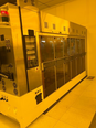


Tap to zoom
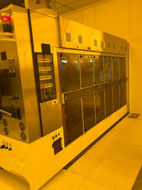

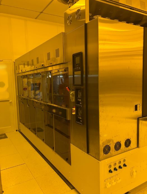
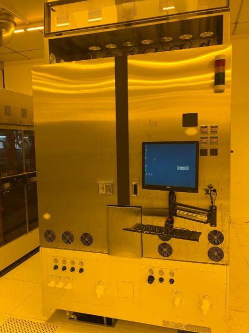
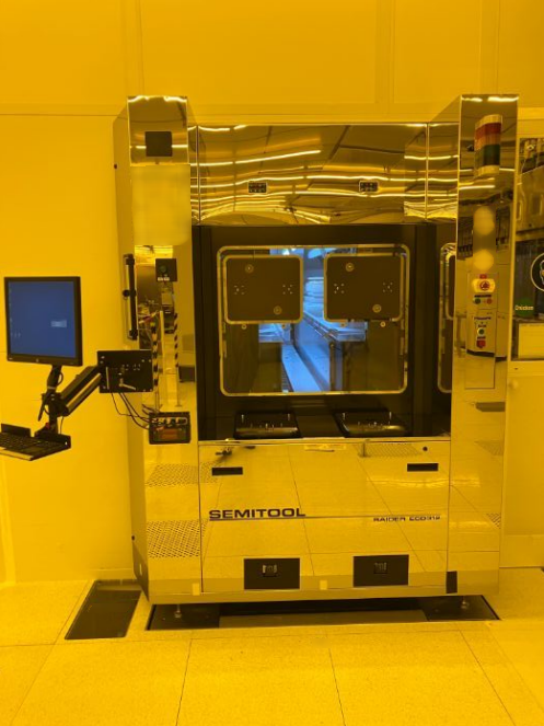
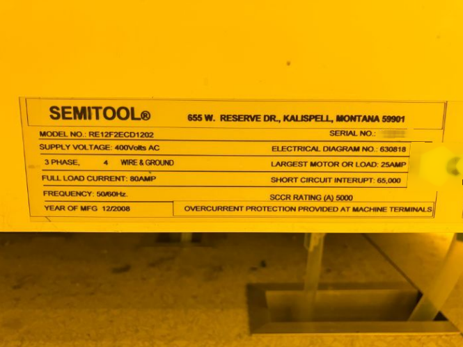
ID: 293777881
Wafer Size: 12"
Vintage: 2008
Wet station, 12"
Mainframe raider
Robot
(2) Front Opening Unified Pods (FOUP)
2008 vintage.
AMAT / APPLIED MATERIALS / SEMITOOL Raider ECD 310, also known as AMAT Raider ECD 310, is a cutting-edge photoresist equipment utilized in semiconductor manufacturing for depositing and patterning thin films onto substrates with high precision and control. This system is specifically designed for electrochemical deposition (ECD) processes, offering advanced capabilities for creating intricate patterns and structures essential for modern integrated circuits and microelectronic devices. One of the key features of SEMITOOL Raider ECD 310 is its high throughput and efficiency, allowing semiconductor manufacturers to achieve fast and cost-effective production of photoresist layers with superior uniformity and quality. This unit is equipped with state-of-the-art automation and control mechanisms to ensure consistent and repeatable patterning results, thereby enhancing the overall yield and performance of semiconductor devices. Raider ECD 310 incorporates a sophisticated deposition chamber with precise temperature and pressure control, enabling the deposition of photoresist materials onto substrates with exceptional uniformity and thickness control. The machine utilizes advanced electrochemical processes to facilitate the selective deposition of photoresist layers on specific regions of the substrate, in accordance with the desired design layout and pattern requirements. Furthermore, APPLIED MATERIALS Raider ECD 310 features a versatile and customizable processing capabilities, allowing semiconductor manufacturers to tailor the deposition parameters and conditions to meet the specific needs of their fabrication processes. This flexibility enables the tool to accommodate a wide range of substrates, including silicon wafers, glass, and flexible substrates, making it suitable for diverse applications in the semiconductor industry. The advanced monitoring and control asset of AMAT / APPLIED MATERIALS / SEMITOOL Raider ECD 310 ensures real-time process optimization and monitoring, enabling operators to track and adjust the deposition parameters to maintain consistent and uniform film properties across the substrate. This level of control is essential for achieving high-quality and reliable photoresist layers required for the fabrication of advanced semiconductor devices with complex geometries and precise dimensions. In addition to its deposition capabilities, AMAT Raider ECD 310 is equipped with advanced patterning and etching features that enable the creation of intricate and high-resolution patterns on the substrate surface. The model incorporates advanced lithography techniques to define the desired pattern layout and transfer it onto the photoresist layer with sub-micron accuracy and precision. Overall, SEMITOOL Raider ECD 310 is a cutting-edge photoresist equipment that offers semiconductor manufacturers a highly advanced and reliable solution for depositing and patterning thin films with exceptional precision and control. With its high throughput, versatility, and advanced process monitoring capabilities, this system is an indispensable tool for the production of next-generation semiconductor devices with ever-increasing complexity and performance requirements.
There are no reviews yet