Used AMAT / APPLIED MATERIALS / SEMITOOL Raider ECD #293809013 for sale
URL successfully copied!


Tap to zoom
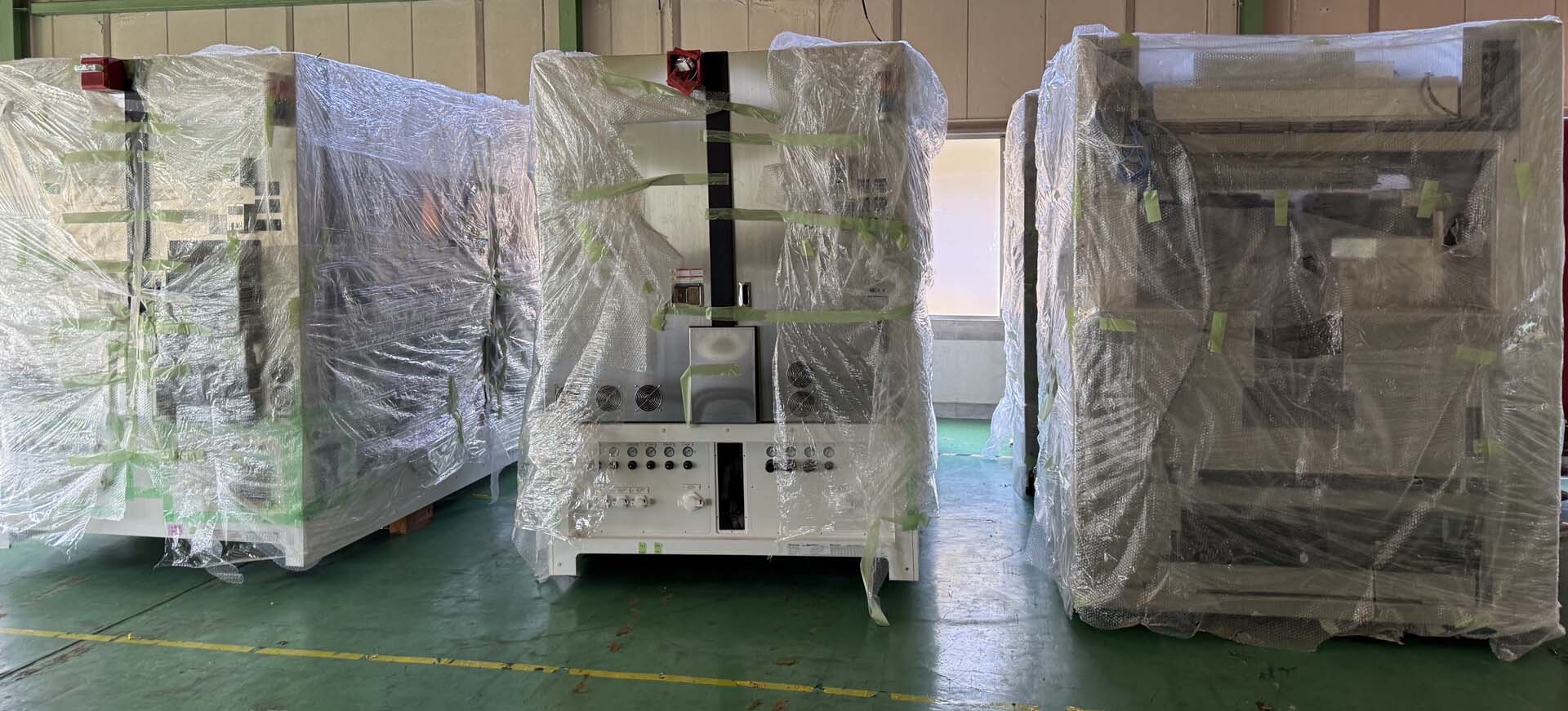

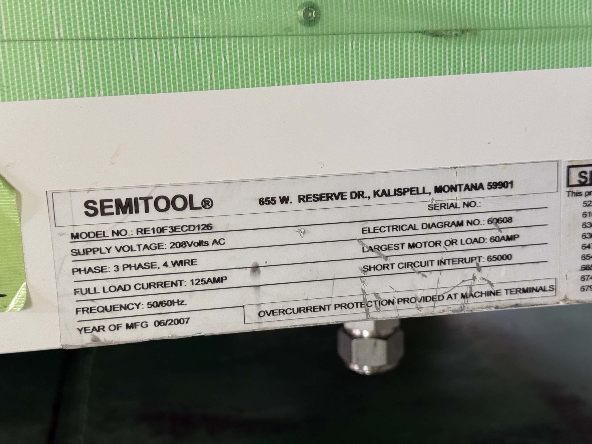
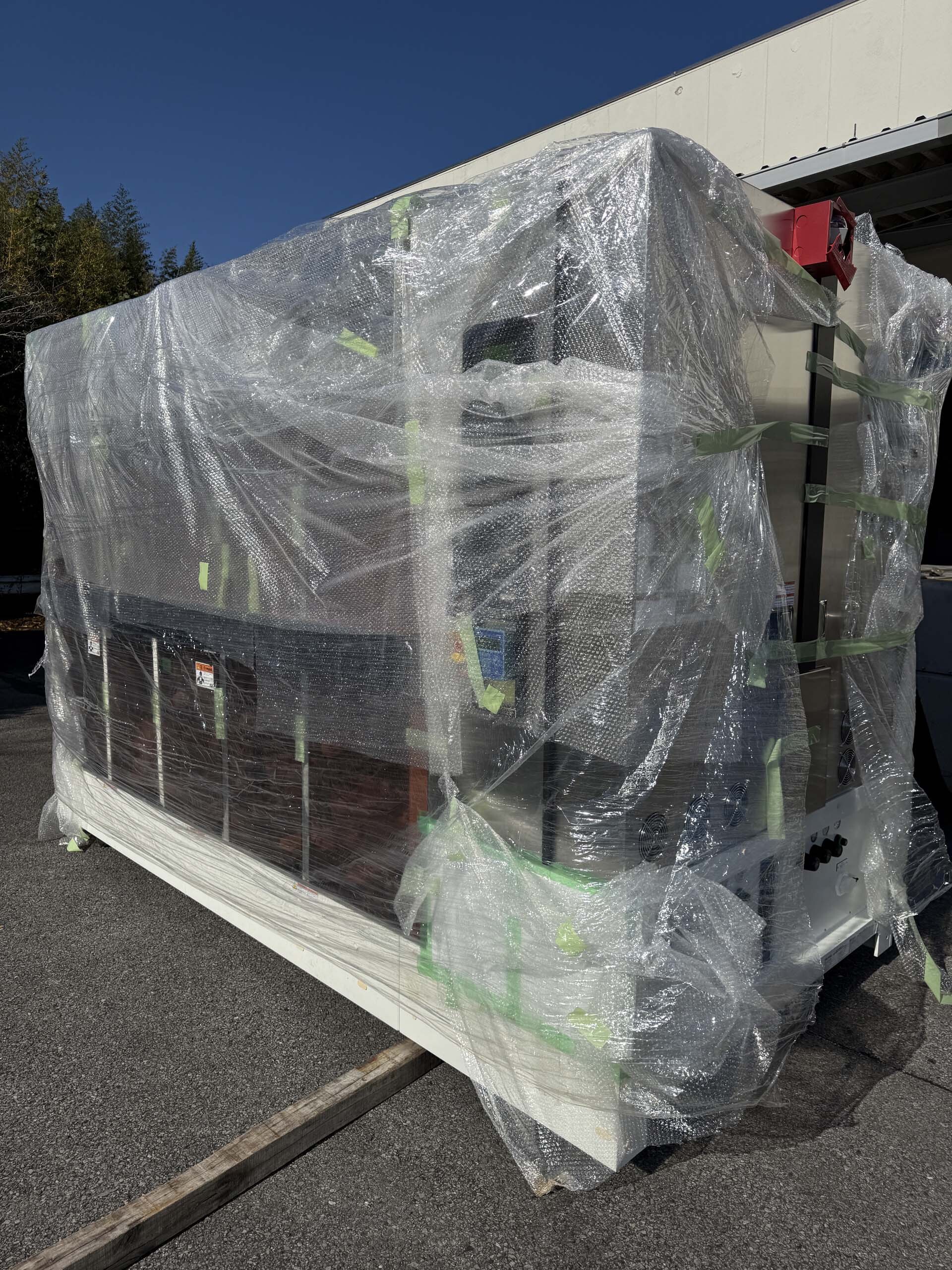
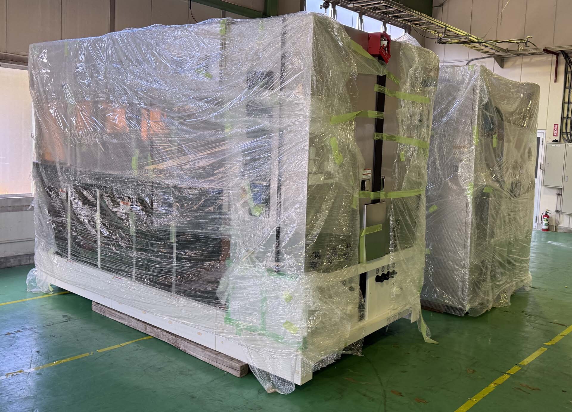
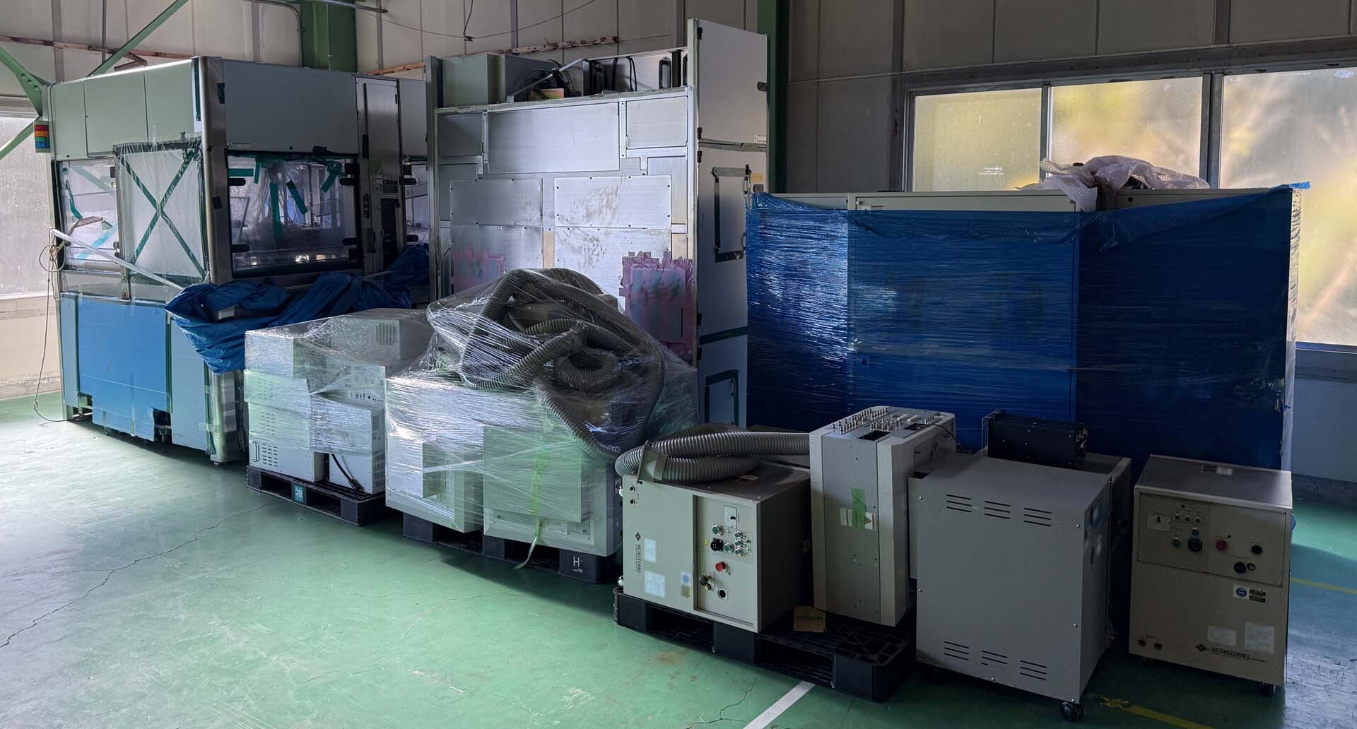
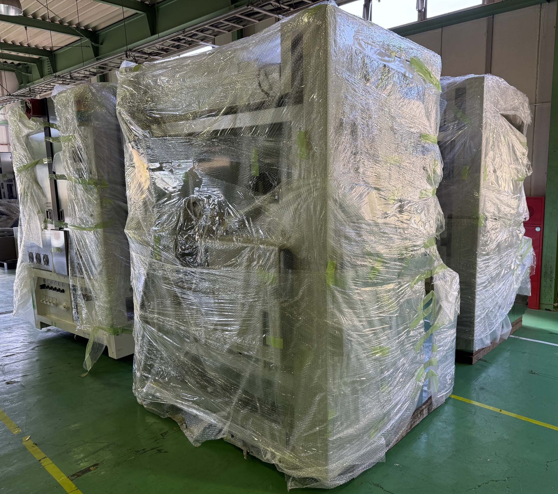
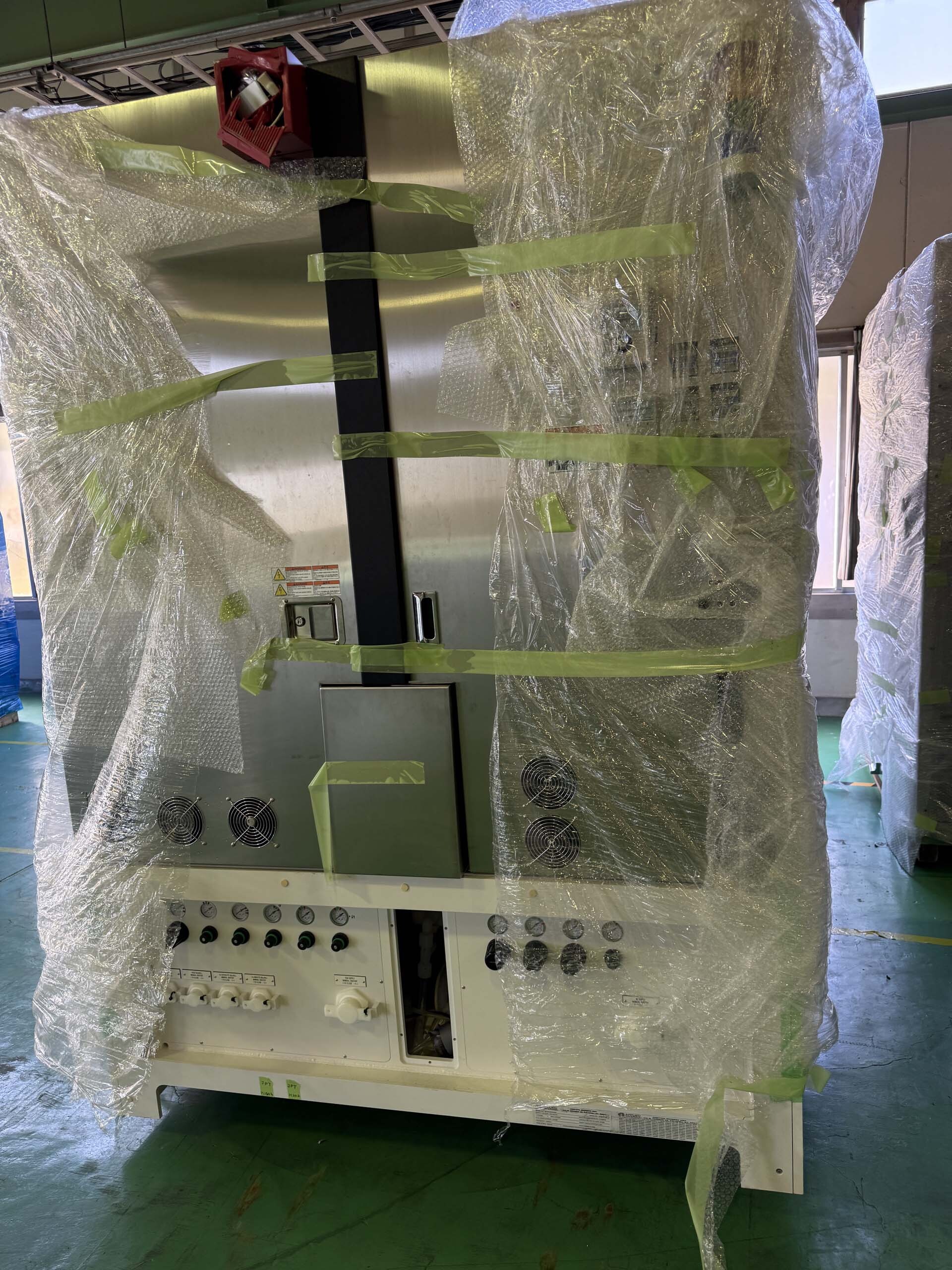
AMAT / APPLIED MATERIALS / SEMITOOL Raider ECD, also known as a photoresist equipment, is a sophisticated tool used in the semiconductor industry for the precise deposition of materials on semiconductor substrates. This system utilizes a process called electrochemical deposition (ECD) to create uniform and controlled layers of photoresist material on wafers, enabling the fabrication of complex semiconductor devices. AMAT Raider ECD unit offers a high level of automation, accuracy, and repeatability, making it an essential component in the production of advanced semiconductor devices. The main function of SEMITOOL Raider ECD machine is to deposit a thin layer of photoresist material onto a semiconductor wafer. Photoresist is a light-sensitive material that is used to transfer patterns onto the semiconductor substrate during the photolithography process. APPLIED MATERIALS Raider ECD tool is capable of depositing photoresist material with high precision and uniformity, ensuring that the resulting patterns are accurate and consistent across the wafer. This is crucial for the successful fabrication of semiconductor devices with intricate designs and features. The key components of Raider ECD asset include a deposition chamber, an electrochemical deposition module, a control model, and software for process control and monitoring. The deposition chamber is a controlled environment where the wafer is placed for the deposition process. The electrochemical deposition module consists of electrodes, electrolyte solution, and a power supply that facilitate the deposition of photoresist material onto the wafer. The control equipment oversees the operation of the system, while the software enables users to set process parameters, monitor performance, and analyze data. AMAT / APPLIED MATERIALS / SEMITOOL Raider ECD unit operates based on the principles of electrochemical deposition, where an electric current is used to drive the deposition of material onto the wafer surface. During the deposition process, the wafer is immersed in an electrolyte solution containing the photoresist material. When a voltage is applied between the electrodes, ions from the electrolyte are attracted to the wafer surface, where they react to form a thin layer of photoresist material. By controlling the deposition parameters such as voltage, current, and time, users can tailor the thickness and uniformity of the deposited layer to meet specific requirements. One of the key advantages of AMAT Raider ECD machine is its ability to deposit photoresist material with high aspect ratios and feature sizes down to the nanoscale. This is essential for the fabrication of advanced semiconductor devices with increasingly smaller dimensions and complex structures. The tool's automation capabilities also contribute to its efficiency and productivity, allowing for high throughput and reduced cycle times in semiconductor manufacturing. In conclusion, SEMITOOL Raider ECD asset is a powerful tool for the deposition of photoresist material in semiconductor manufacturing. Its advanced capabilities in electrochemical deposition, automation, and process control make it an indispensable asset for the production of cutting-edge semiconductor devices. By enabling precise and uniform deposition of photoresist material, APPLIED MATERIALS Raider ECD model plays a critical role in the successful realization of complex semiconductor designs and technologies.
There are no reviews yet