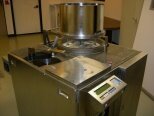
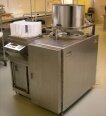
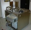
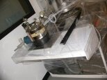
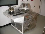
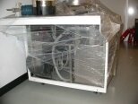
Used APT 3025 #49738 for sale
URL successfully copied!
Tap to zoom





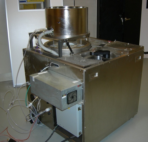

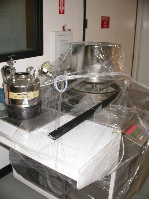

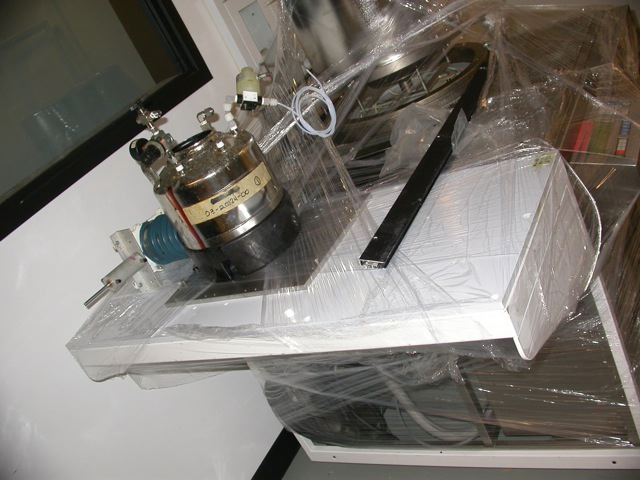

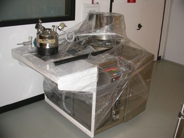

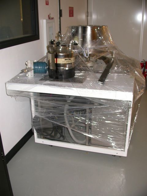

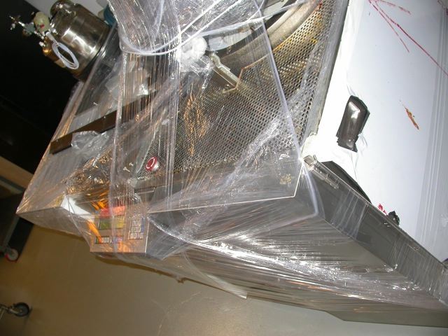

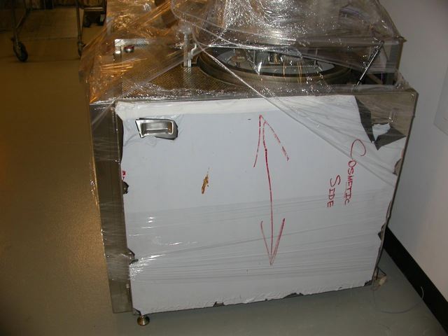

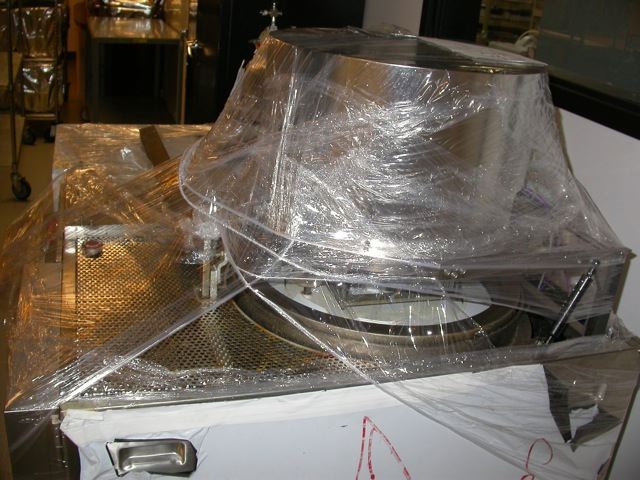


ID: 49738
Wafer Size: 12"
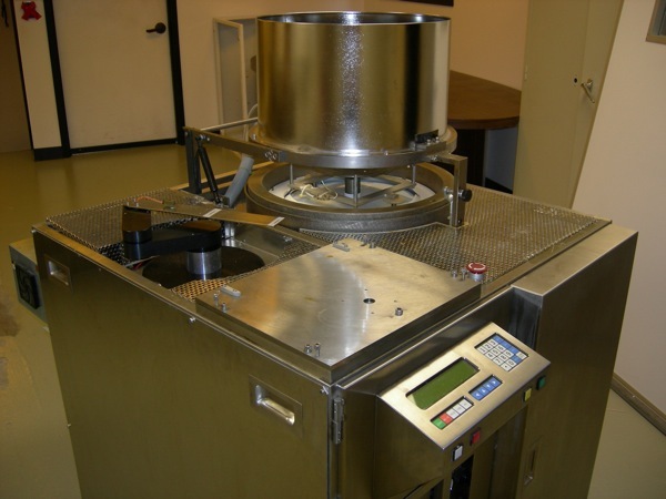
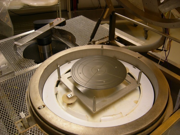
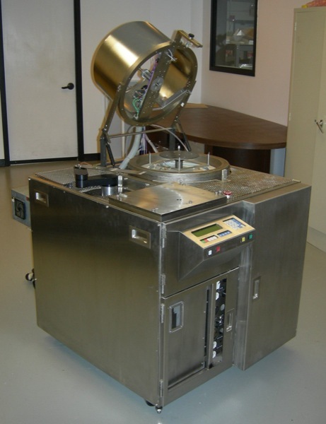
Auotmated Single wafer spin coater, 12"
Used for photoresist and polyimide
Unit has programmable cycles
Unit has a robot to load wafers from a cassette
Automatic coating of up to 12" round substrates (wafer)
Footprint is approximately 3'x5'
Stainless steel frame and stainless steel skins
Robotic handling system for pick-and-place substrate handling
Direct drive brushless servo motor with spin speed control of 50-3500 RPM
1% (max. speed dependent on substrate mass)
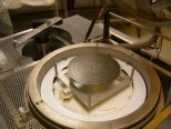
Metal process chamber with removable polypropylene process insert
Selection of up to 3 different dispense systems
Programmable dispense arm for static dispensing
Removable polypropylene process cup
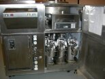
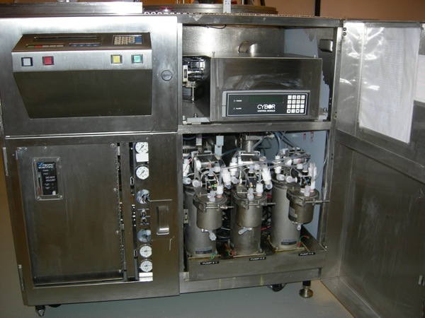
Fluid and pneumatic control panel for flow control, pressure control and valves
Microprocessor controller based on STD bus system for 99 programmable recipes
Alphanumeric LCD display unit with 4 lines x 40 characters
Menu driven software including diagnostics
Photo resist Dispense System consisting of:
Cyborpump resist dispense
Filter
Pump Controller
Chuck Cleaning System consisting of:
Programmable chuck cleaning system
Solvent nozzle
Valve
Solvent Canister Kit, including:
Pressurized 2 gallon solvent canister
regulator
Filter
Valve
Maximum pressure for N2 = 60 PSI
As-is.
APT 3025 is a high-performance photoresist equipment that is designed to be used for the fabrication of integrated circuit (IC) components in the semiconductor industry. It is an advanced etching system which utilizes a photoresist coating as a protective layer between the metal layer and the substrate layer. This photoresist layer is designed to be capable of absorbing and holding onto photons which travel through the device, thus providing a barrier between the substrate layer and the metal layer. 3025 photoresist unit is comprised of three distinct components: a photoresist coating, a substrate transfer machine, and a UV-light source. The photoresist coating is a specialized material that is capable of absorbing visible light so that a pattern of lines or shapes can be formed with precision. This layer is then transferred to the substrate in an uniform manner with the help of a substrate transfer tool. The UV-light source is used to expose the photoresist layer with ultraviolet radiation which causes the lines and shapes to be etch into the substrate layer. APT 3025 asset utilizes a variety of components to ensure that the photoresist layer is of the highest-quality and highest-integrity. For example, the substrate transfer model is designed to treat the photoresist layer with a special chemical treatment in order to ensure that the photoresist layer is homogeneous and free of any imperfections. Furthermore, the UV-light source is specially designed to provide the optimal amount of radiation emission for the desired task. In the semiconductor industry, accuracy and precision are crucial factors for producing high quality IC components. 3025 photoresist equipment is designed to meet these needs, as it allows for the extremely accurate placement and etching of the photoresist layer. This state-of-the-art system is able to create intricate patterns with very thin lines and an extremely high feature definition which provides a very high level of accuracy in the fabrication process. APT 3025 also incorporates several other advanced features that allow it to perform more tasks than just etching. For example, it is also equipped with a resist stripping unit which is used to remove any excess photoresist that is left over after the etching process. Additionally, it is also capable of pattern optimization so that it may be adapted to any given application. Furthermore, features such as variable scan head speed and variable exposure times, enable the process to be tailored to suit the specific needs of each project. Overall, 3025 photoresist machine is a powerful and highly effective tool for fabricating IC components with accuracy, precision, and efficiency. Its advanced features, such as the resist stripping tool, variable scan head speed and variable exposure times, make it an extremely flexible asset which can be optimized for performing various tasks with ease. With its capabilities, this model is a valuable asset for the semiconductor industry and is sure to be an important part of the manufacturing landscape for years to come.
There are no reviews yet
