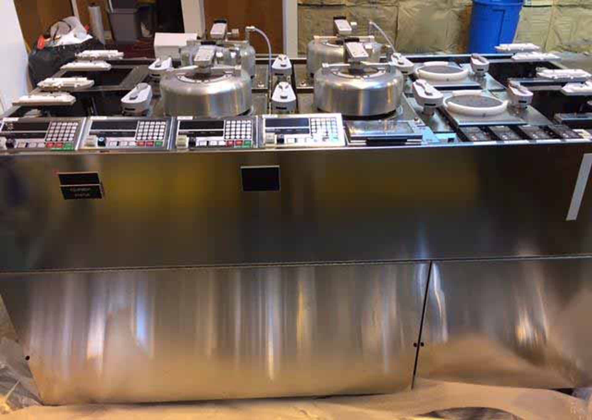
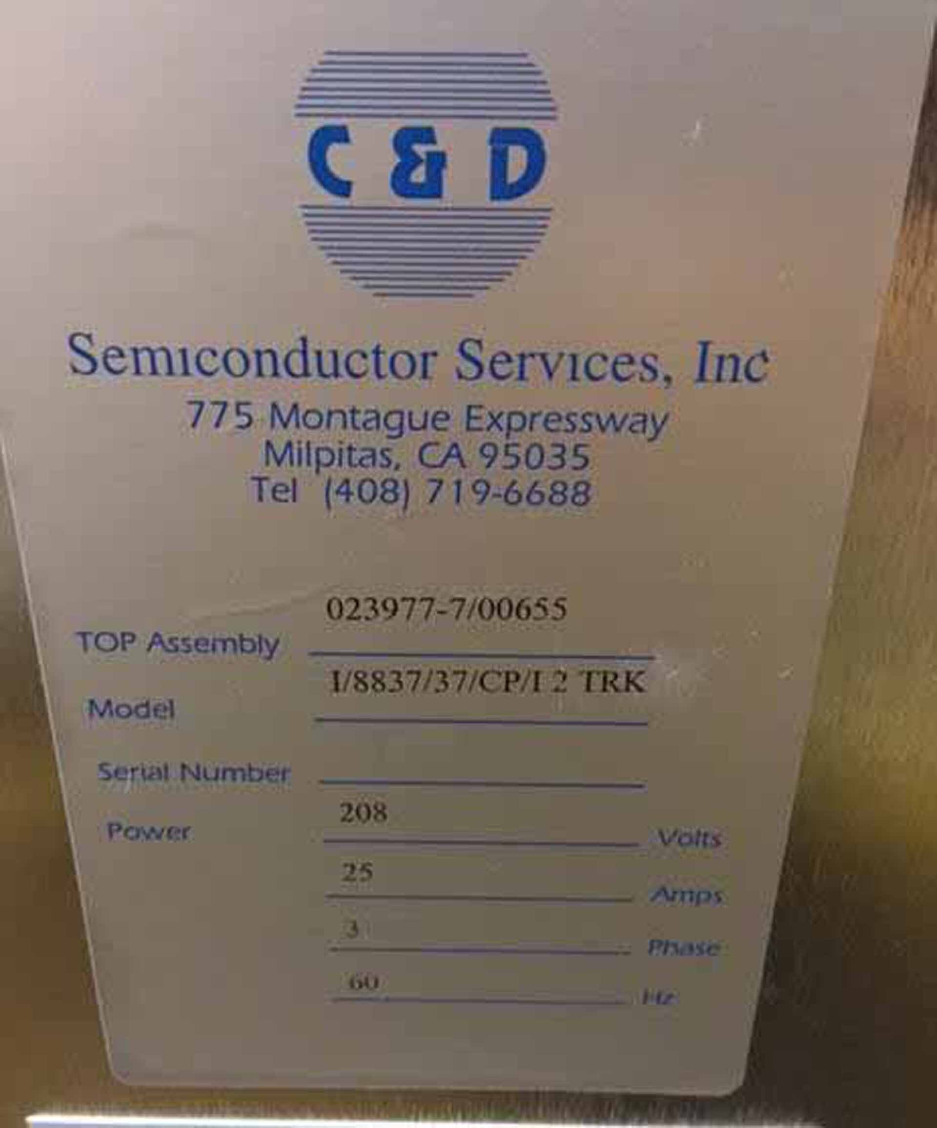
Used C&D SEMI I/8837/37/CP/I 2 TRK #9205718 for sale
URL successfully copied!
Tap to zoom


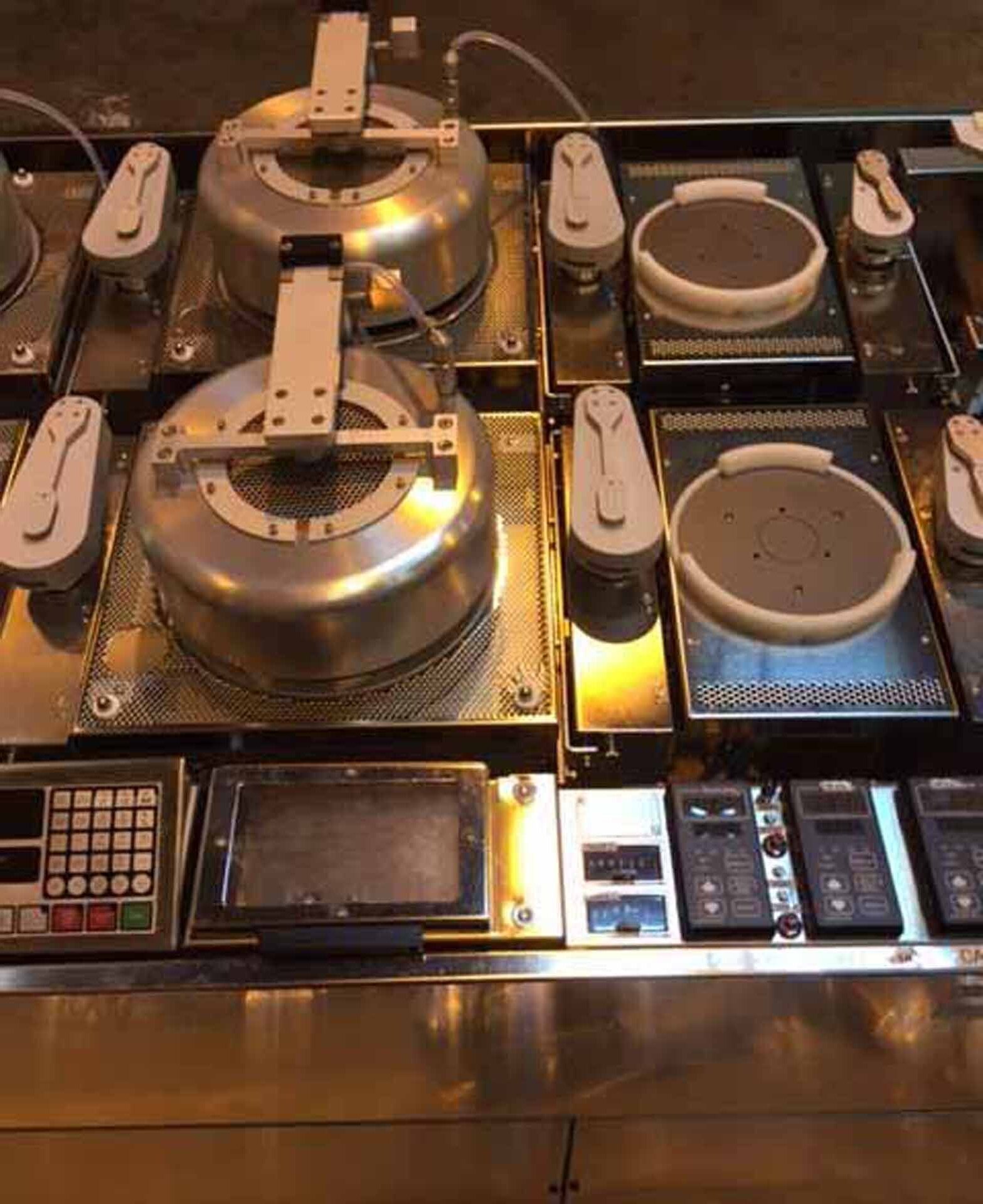
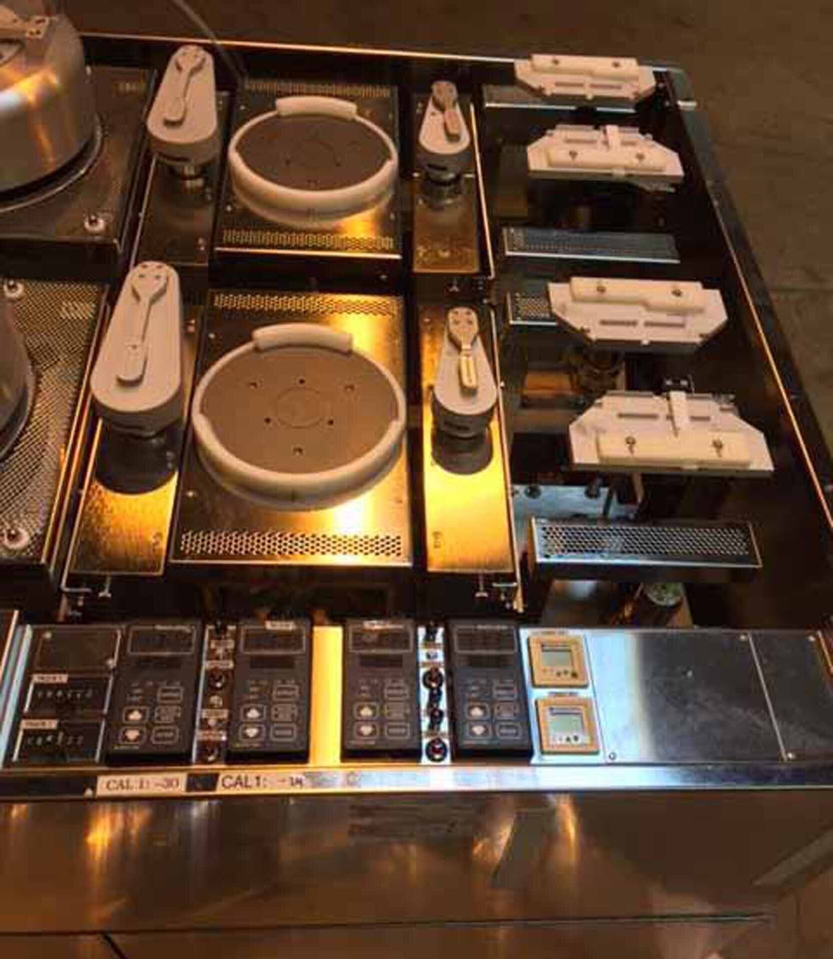
C&D SEMI I/8837/37/CP/I 2 TRK photoresist equipment is a versatile, easy-to-use and robust photolithography system for the production of highly accurate masks, wafers, moldings and printed circuit boards. It is uniquely designed for the advancement of the semi-conductor industry by offering improved cost-effectiveness, precision, and a wide variety of photographic processes for precise manufacturing results. C&D SEMI I/8837/37/CP/I 2 TRK photoresist unit is specially designed for the semiconductor industry to produce high-precision masks and wafers. It contains two tracks for the masking and patterning stages of a production. The first track utilizes five images - the top frame, a back exposure, a diffusion mask, a pattern transfer plate, and a water-loaded glass slide -while the second track consists of five more images - the top frame, a back exposure, a contamination mask, a pattern transfer plate, and a dry glass slide. The top frame is used to expose the dry glass slide onto which the photographic mask is drawn. The back exposure is used with the diffusion mask to ensure depth of field while presenting the mask's pattern onto the glass slide. The contamination mask is used to eradicate the chemicals present on the glass slide. The pattern transfer plate is used to produce an optically-corrected image on the glass slide while the water-loaded glass slide is used to guarantee perfect adhesion for the photographic mask and the print of the pattern onto the board. C&D SEMI I/8837/37/CP/I 2 TRK photoresist machine is equipped with precision optics and laser-guided alignment tools. Its top-class construction makes it reliable and capable of achieving high-resolution results. With improved advances in printing clarity and excellent adhesion of all the layers, it is the most efficient and cost-effective photolithography tool for the production of highly accurate masks, wafers, moldings and printed circuit boards. It is also the perfect choice for advanced photolithography processes including advanced thin-film electronics. C&D SEMI I/8837/37/CP/I 2 TRK photoresist asset provides superior resolution consistency by incorporating a uniform operational pattern. It also ensures greater image precision with its advanced alignment tools that allow for small adjustments even after long hours of use. Moreover, it guarantees robust manufacturing processes with its anti-contamination feature which prevents irregularities even with repeat exposures. The model thus offers the best quality masks, wafers, moldings and printed circuit boards for the production of today's advanced electronic devices.
There are no reviews yet


