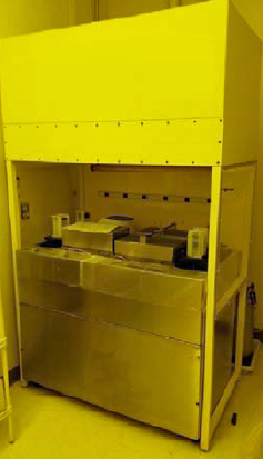
Used CUSTOM Custom #9097575 for sale
URL successfully copied!
Tap to zoom


A photoresist system is a substrate processing technique that uses light-sensitive materials to produce patterns on photoresist substrates. CUSTOM Custom photoresist systems are used in the electronic industry for a variety of tasks including developing fine pattern geometries, aligning and transferring patterns on various media, and etching components into a substrate. Photoresist systems work by exposing a photosensitive layer to a pattern of light. This layer of photoresist material will darken upon exposure to the appropriate wavelengths of light. By controlling the exposure to light, fine patterns are produced on the photoresist layer that are not easily accomplished with more standard techniques. Custom photoresist process begins with the preparation of the original photoresist material. This typically involves the creation of a relatively large size positive or negative image of the desired circuit pattern. CUSTOM Custom pattern can then be transferred to a photoresist substrate in a number of ways. A printed film may be used, or a direct write process may be applied. Once the pattern is on the substrate, the photoresist is then exposed to a particular wavelength of light. The photoresist acts like a photographic film, darkening any area that is subject to the light. This darkening process is known as photolitography. Following exposure, the photoresist material can then be further processed. Development of the photoresist can be done using proprietary development solutions or solvents. This results in the etching of the photoresist layer just where it had been exposed to the light, thus creating a pattern on the substrate. Once the desired pattern is developed, the substrate can then be manipulated further by etching, chemical removal or other processes. It is also possible to use the photoresist system to produce components such as integrated circuits or other types of components. After etching, the photoresis layer can then be stripped away and reused. A Custom photoresist system allows for the production of extremely fine and complex patterns that are not easily achievable with other types of processes. It is a relatively inexpensive way to develop intricate patterns on substrate materials, and it is a key part of the modern electronics manufacturing process. Its use in the fabrication of components makes it an invaluable tool for the electronic industry.
There are no reviews yet