Used DNS / DAINIPPON 80B #9400647 for sale
URL successfully copied!
Tap to zoom
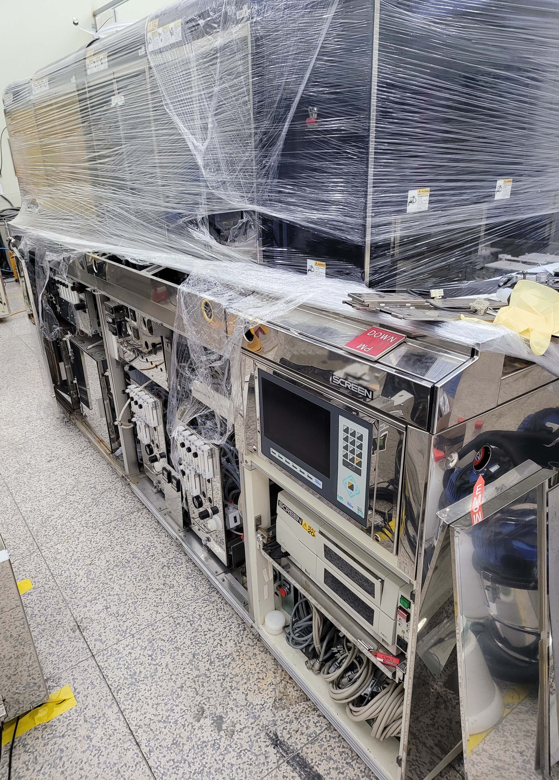

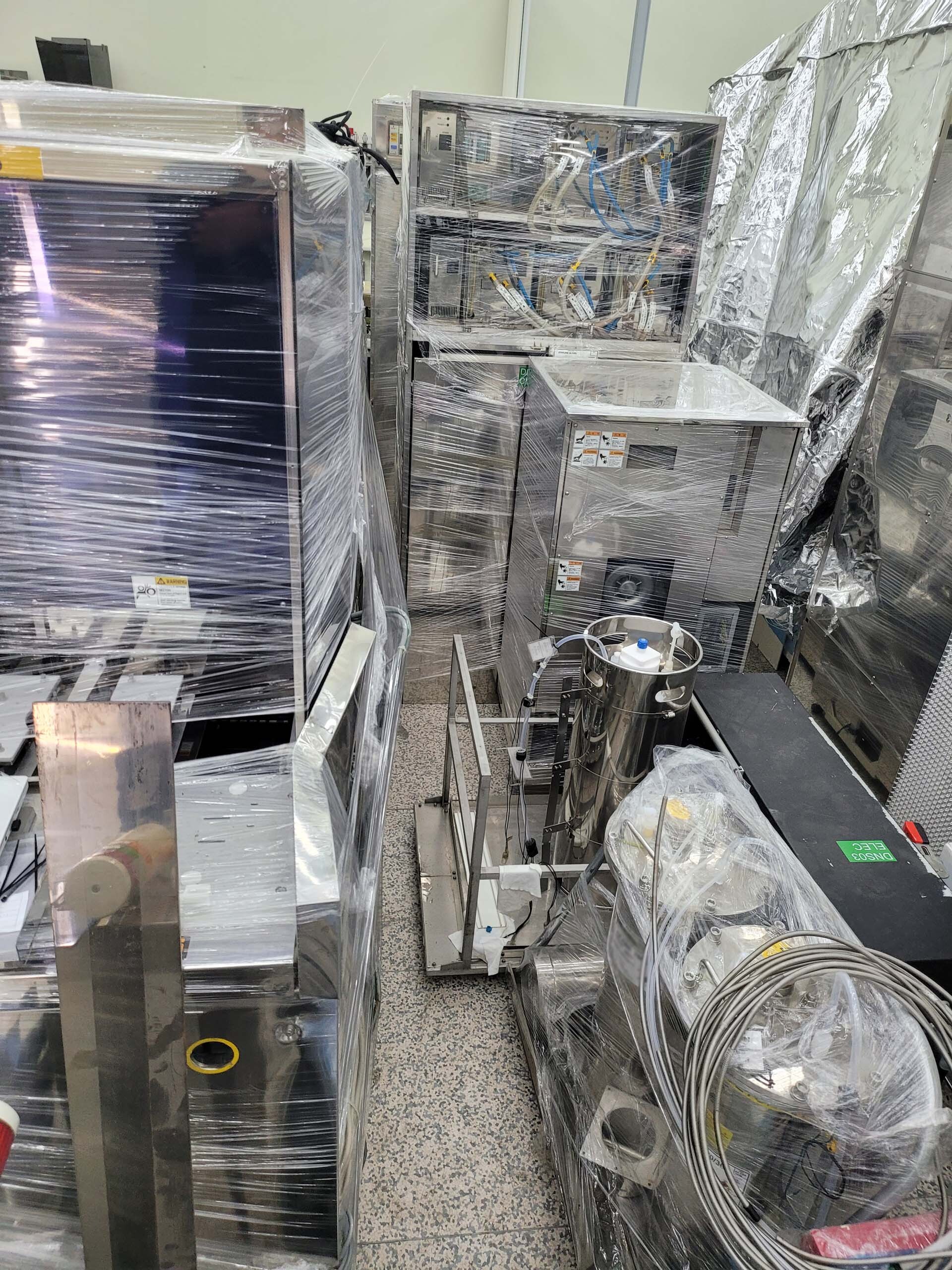

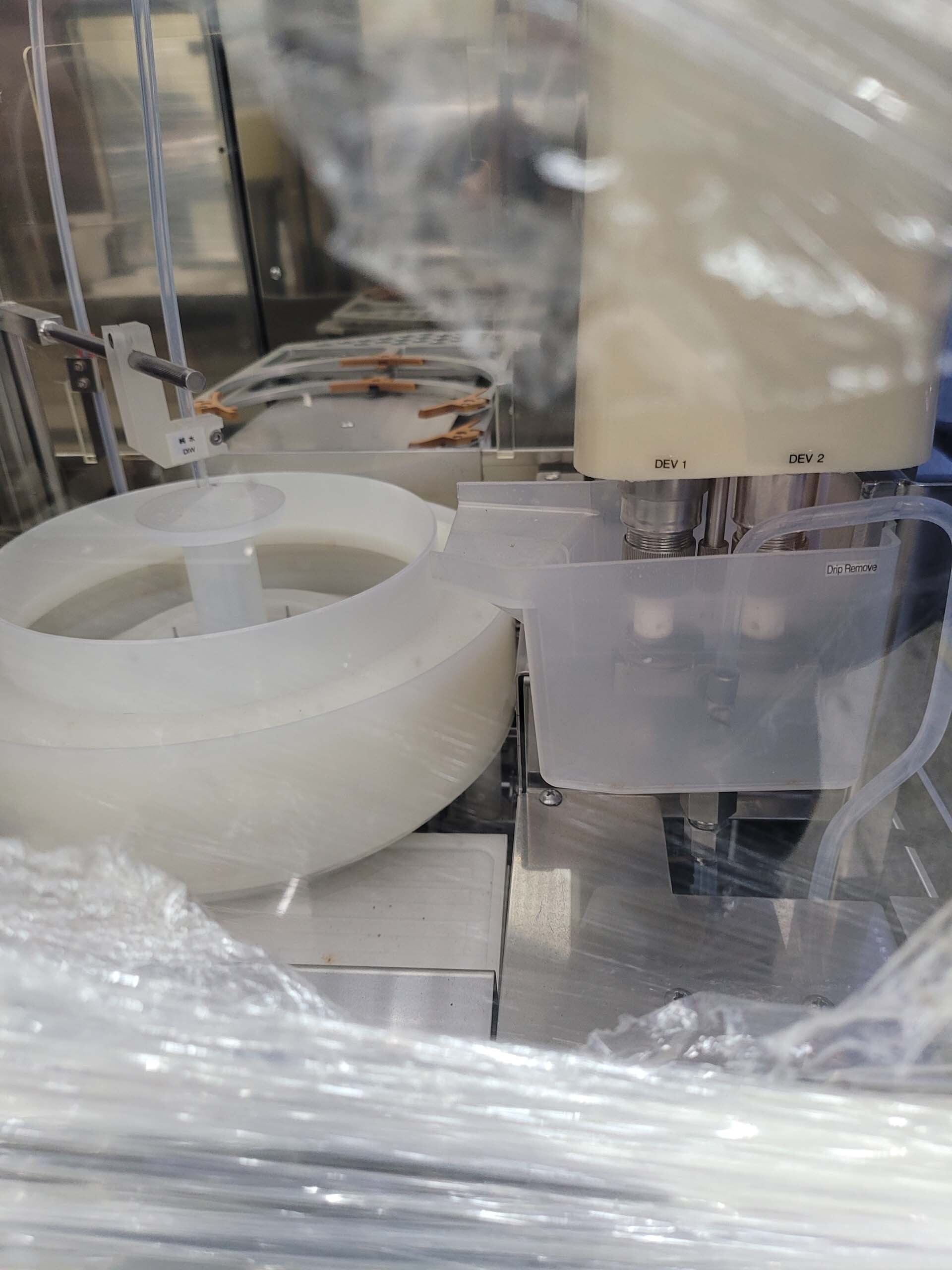

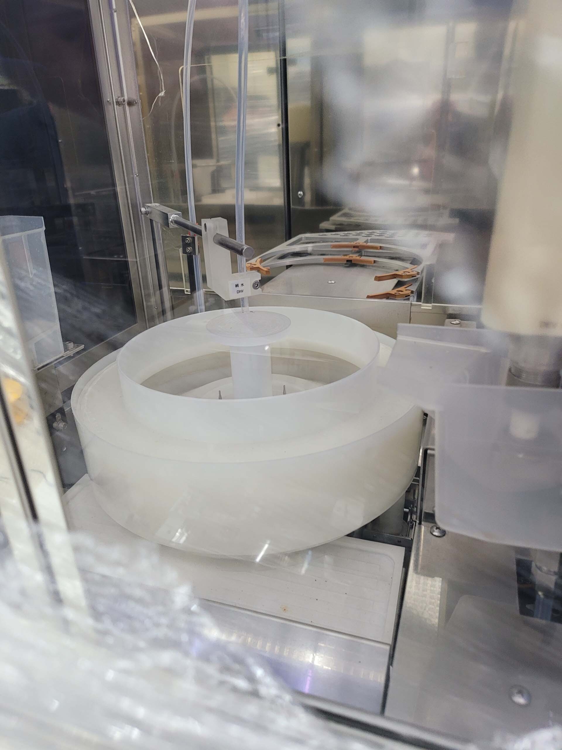

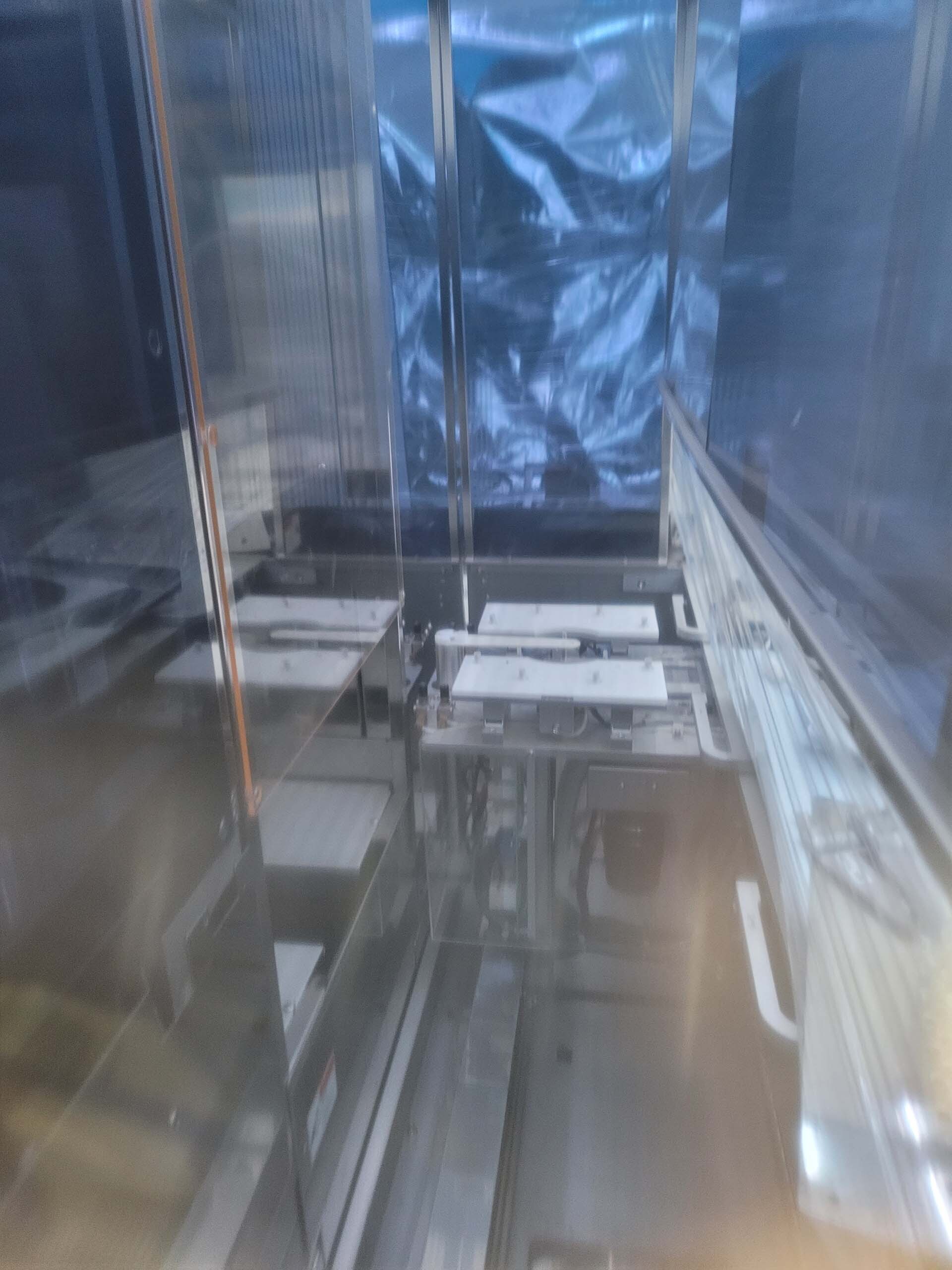

ID: 9400647
(2) Coater / (2) Developer system
Type: Open cassette, 8"
THC
Chemical cabinet
ETU
Coater:
(6) PR Nozzles unit per spin (IWAKI Bellow pump)
EBR
RRC Nozzle
Cup rinse
Back rinse
Developer:
DEV1 / (2) Nozzles
Pre-wet nozzle
DI Rinse 1/2
Back rinse
HP
CP
LPAH / AH.
DNS / DAINIPPON 80B is a photoresist equipment designed for semiconductor device fabrication and designed for high-quality resist patterning of devices. It is a sophisticated system that is able to precisely control the exposure and development of photoresist layers on specific substrates. DNS 80B Photoresist Unit utilizes a pulsed laser source, a precise set of masking and development technologies, and a substrate heating application to produce optimal results. The machine is capable of patterning substrates up to six inches in diameter with a precise resolution of as low as 10 microns in width. The tool also offers unique features that support precise alignment of the photoresist layer over the substrate, as well as controlled exposure of the photoresist without harm to the substrate. To begin the process, the substrate must be cleaned and treated before the photoresist is applied. After the substrate is prepared, the masking stages take place in order to form the desired pattern. The laser source of DAINIPPON 80B applies the precise amount of light energy onto the selected substrate, heating and curing the photoresist layers and creating detailed levels of patterning within the photoresist. The photolithography begins once the laser source has been triggered and adjusted. The areas of the substrate exposed to the light source will have hardened, while the areas hidden with the photomask will remain soft. Once the photoresist is then developed, the soft and hard photoresist areas are exposed, allowing it to be etched away in different portions of the substrate. The Heating Application in the asset acts as a post-development process. It promotes precision when etching away the photoresist, as well as protection of the substrate material. It also helps to completely remove all undesired photoresist areas before the device is ready to move onto the next manufacturing step. 80B is a powerful and precise tool for semiconductor device fabrication. Its laser source, precise masking, and substrate heating capabilities make it an ideal model for achieving high accuracy in the photoresist patterning process. It is an essential element in the development of advanced electronic devices and continues to be an important technology for semiconductor device manufacturing.
There are no reviews yet


