Used DNS / DAINIPPON DUOI #293702044 for sale
URL successfully copied!









Tap to zoom
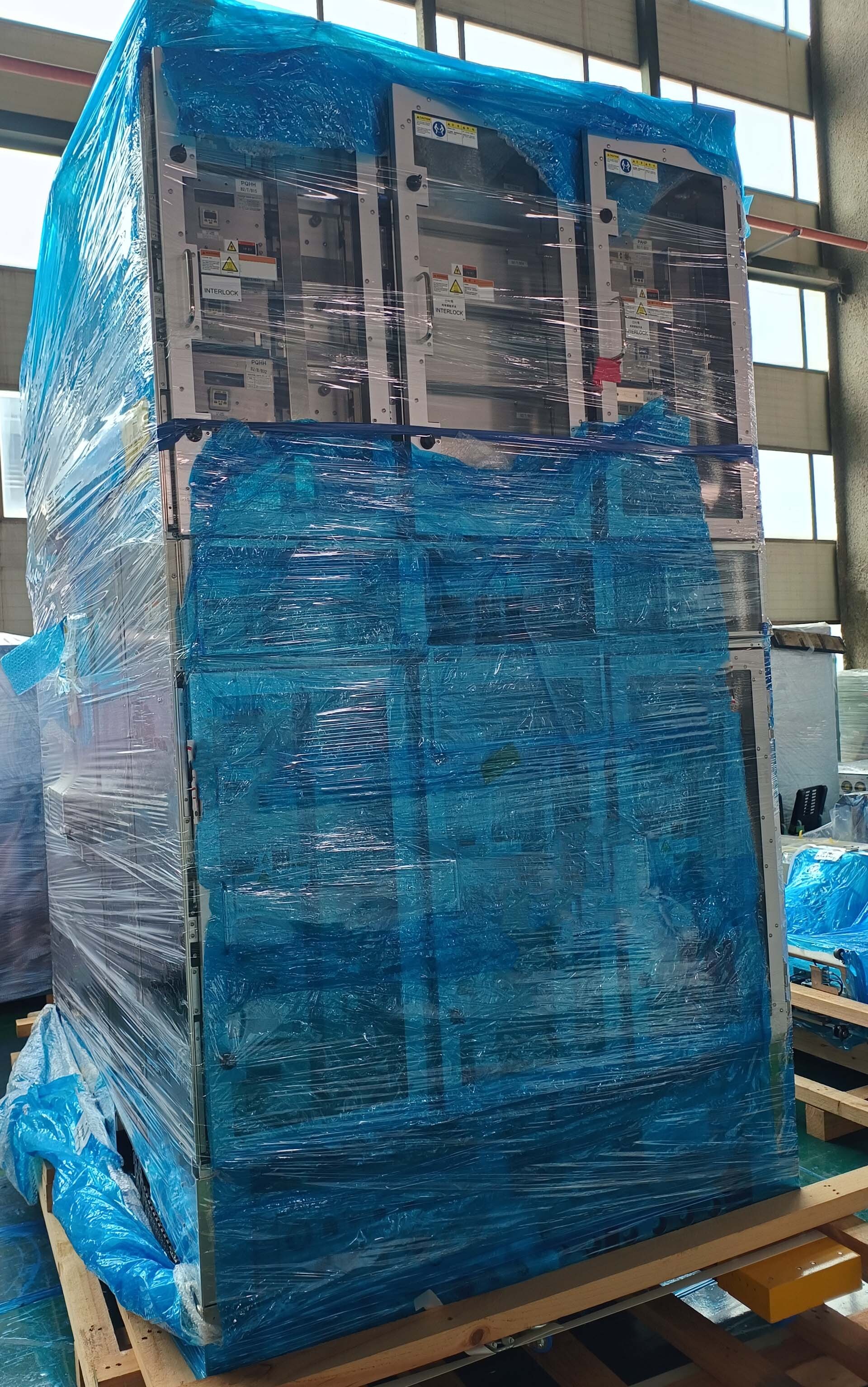


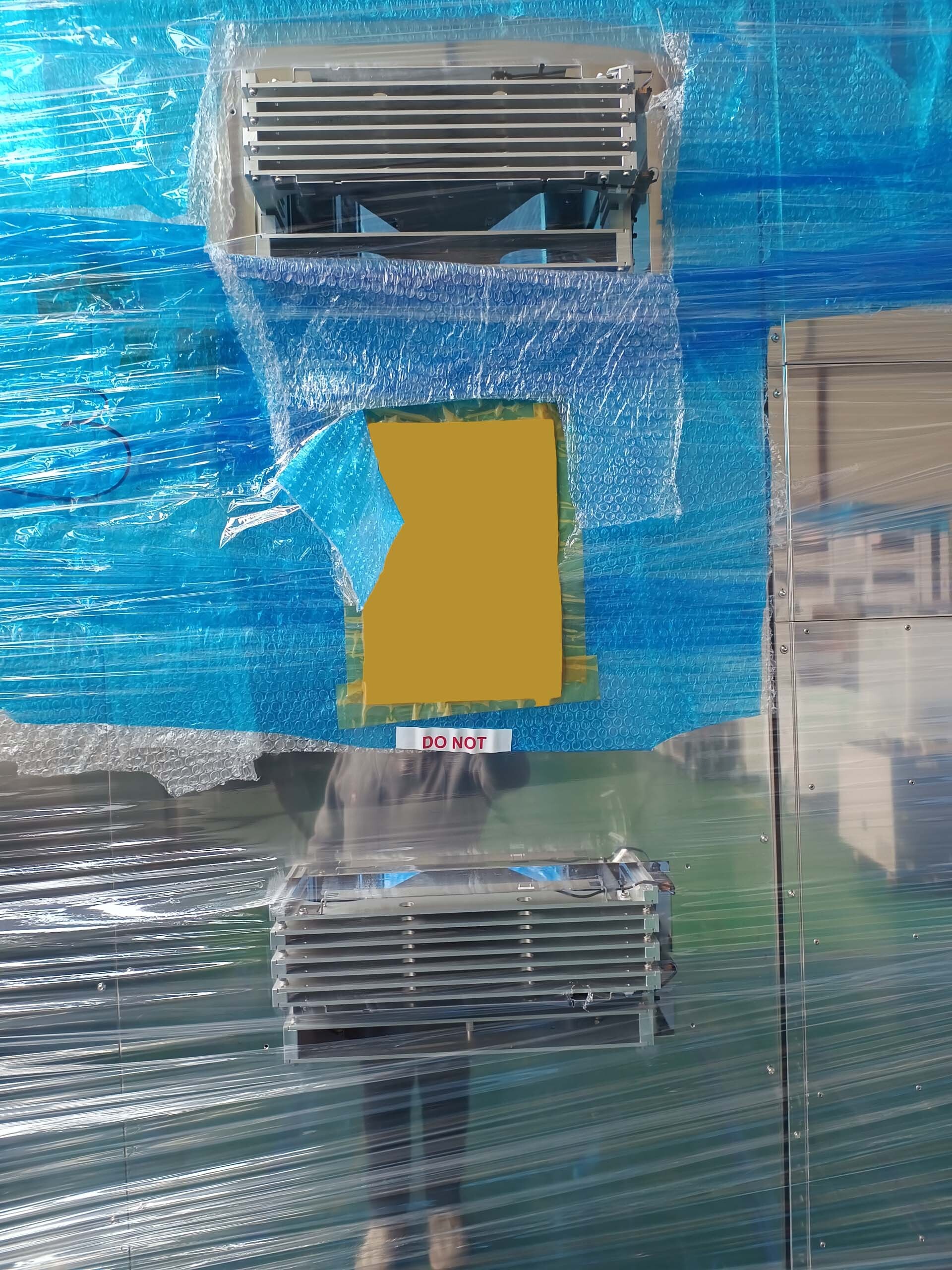

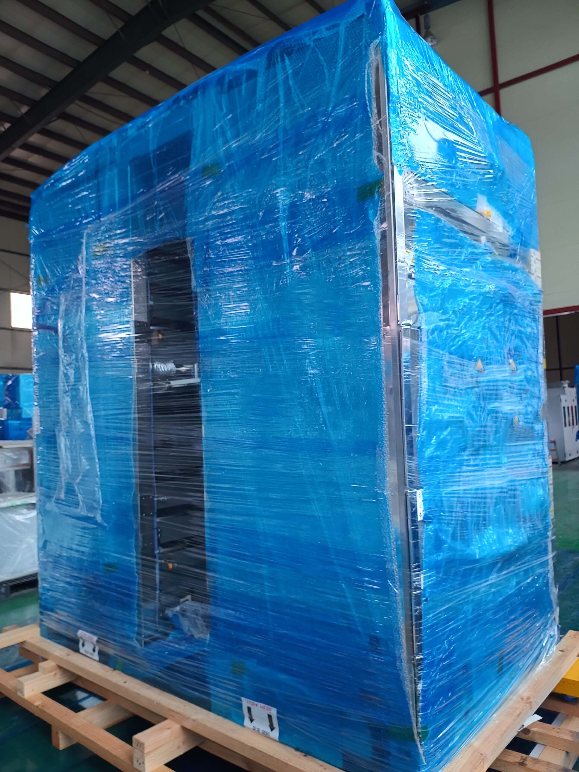
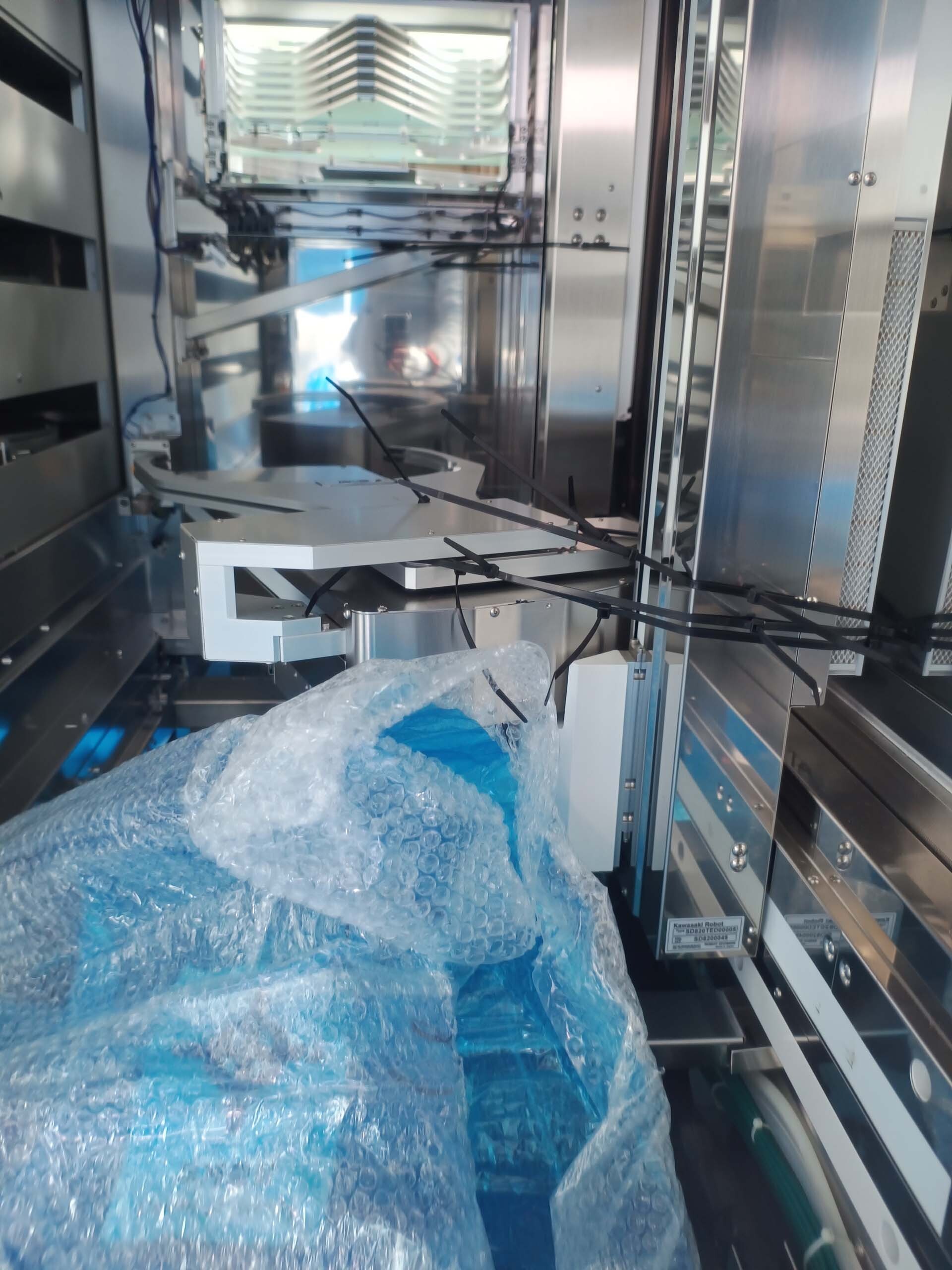
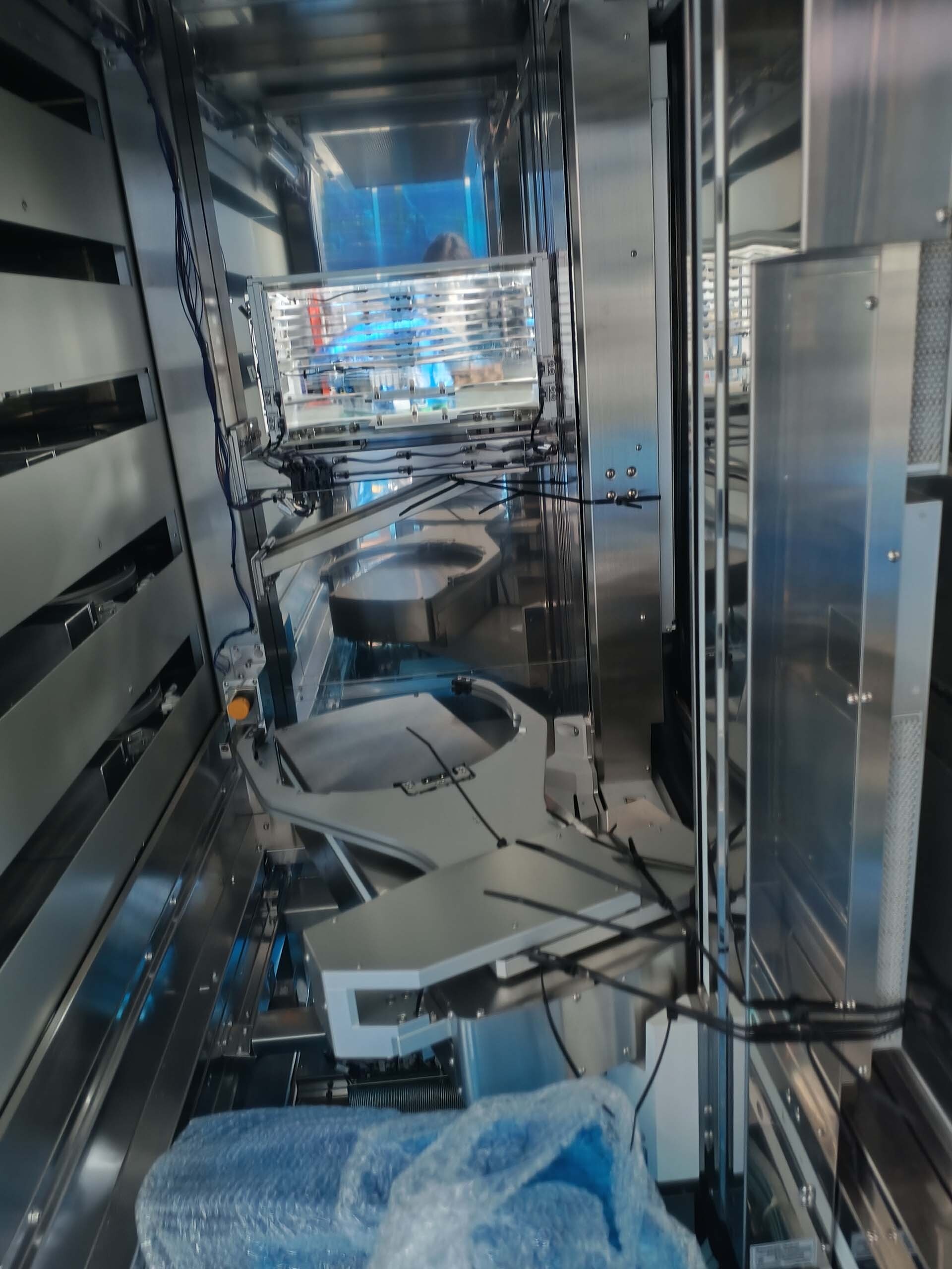

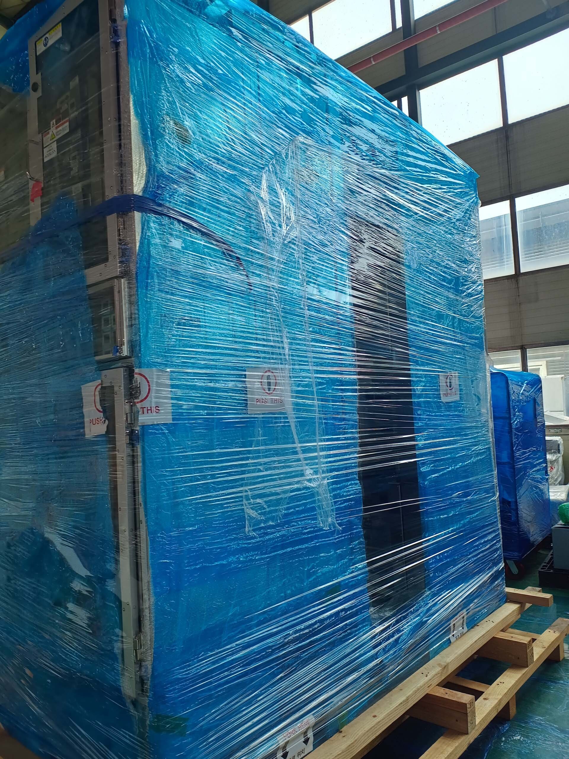
I believe there might be a misunderstanding in the name you provided as "DNS / DAINIPPON DUOI," as it does not seem to correspond to any commonly known photoresist system within the semiconductor industry. However, I can provide you with a general overview and technical details about photoresist systems used in semiconductor manufacturing. Photoresist is a key material used in the fabrication of semiconductor devices, serving as a light-sensitive coating that is patterned using photolithography to define the circuit patterns on semiconductor wafers. The photoresist system consists of various components such as a photoactive compound, a resin matrix, and solvent systems that help in achieving the desired patterning and resolution on the wafer surface. The photoresist process begins with the application of a liquid photoresist material onto the semiconductor wafer substrate. This can be done through spin coating, spray coating, or other deposition methods to ensure a uniform and smooth coating thickness. The coated wafer is then prebaked to evaporate the solvent and improve adhesion of the photoresist film to the wafer surface. Next, the wafer is exposed to ultraviolet (UV) light through a photomask, which contains the desired circuit pattern to be transferred onto the wafer. The photoactive compound in the resist undergoes a chemical reaction upon exposure to light, leading to a change in solubility properties. This allows for selective removal of either the exposed or unexposed regions of the resist during the development process. After exposure, the wafer undergoes a development step where it is immersed in a developer solution that dissolves the unexposed areas of the resist, revealing the underlying wafer surface. The wafer is then rinsed and dried to complete the patterning process. The patterned resist layer serves as a mask for subsequent etching, deposition, or other processes to transfer the pattern into the underlying layers of the semiconductor device. In terms of technical specifications, photoresist systems are characterized by parameters such as sensitivity, resolution, contrast, and adhesion strength. Sensitivity refers to the amount of light energy required to induce a chemical change in the resist, with higher sensitivity allowing for faster exposure times. Resolution defines the minimum feature size that can be resolved on the wafer, while contrast indicates the differentiation between exposed and unexposed regions of the resist. Adhesion strength is crucial for ensuring that the resist remains intact during subsequent processing steps, preventing pattern deformation or delamination. Additionally, considerations such as chemical compatibility, thermal stability, and environmental impact play a significant role in the selection of a photoresist system for specific semiconductor manufacturing applications. In conclusion, photoresist systems are essential components in the semiconductor industry, enabling the precise patterning of circuit structures on semiconductor wafers. By understanding the underlying principles and technical aspects of photoresist materials and processes, semiconductor manufacturers can achieve high-performance and reliable fabrication of advanced semiconductor devices.
There are no reviews yet