Used EVG / EV GROUP 105 #293761363 for sale
URL successfully copied!
Tap to zoom
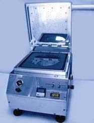

ID: 293761363
Wafer Size: 2"-12"
Bake module, 2"-12"
Manual wafer loading
Hot plate bake temperature: 150°C
SEMI Standard
Hot plate cover
Simultaneous bake:
Up to (9) wafers
Up to 100 mm size
Bake process: Soft / Post exposure
Wafer fixation via vacuum
Load and unload pneumatic lift pins
Temperature controller
Power supply
Solvent exhaust connection
Standalone.
EVG / EV GROUP 105 is a state-of-the-art photoresist equipment designed for high-precision lithography processes in the semiconductor and microelectronics industries. This advanced system combines cutting-edge technology with industry-leading performance to meet the demands of next-generation device fabrication. EVG 105 is part of EVG comprehensive portfolio of lithography equipment and solutions, leveraging the company's expertise in nanotechnology and wafer processing. At the core of EV GROUP 105 unit is its sophisticated exposure module, which utilizes advanced optics and precise alignment mechanisms to achieve submicron resolution and alignment accuracy. This enables the machine to pattern photoresist materials with exceptional precision, making it ideal for the production of advanced semiconductor devices with sub-100 nm feature sizes. The tool's exposure module is equipped with multiple light sources, including UV and DUV sources, to provide flexibility in the selection of photoresist materials and exposure wavelengths. 105 asset features a versatile chucking mechanism that supports a wide range of wafer sizes, including 150 mm, 200 mm, and 300 mm wafers. This flexibility allows manufacturers to use the model for various device applications and production requirements. The chucking mechanism also ensures excellent flatness and alignment of the wafers during the lithography process, minimizing the risk of alignment errors and defects in the patterned structures. In addition to its precision exposure capabilities, EVG / EV GROUP 105 equipment offers advanced process control features to ensure uniformity and repeatability in the lithography process. The system is equipped with real-time monitoring and feedback mechanisms that enable users to optimize process parameters and alert them to any deviations from the desired specifications. This level of control is essential for achieving high yields and device performance in semiconductor manufacturing. EVG 105 unit is also designed for high-throughput production environments, with automation capabilities that streamline the lithography process and reduce cycle times. The machine can be integrated into multi-tool clusters and production lines, enabling seamless transfer of wafers between processing steps. This scalability and automation enable manufacturers to increase throughput and efficiency while maintaining high-quality standards in device fabrication. Moreover, EV GROUP 105 tool is supported by a comprehensive software suite that provides users with intuitive control interfaces, process recipes, and data analysis tools. The software enables users to easily program and optimize lithography processes, monitor asset performance in real-time, and analyze the quality of patterned structures. This data-driven approach allows users to make informed decisions and continually improve the lithography process for better device performance and yield. In conclusion, 105 is a cutting-edge photoresist model that offers unmatched precision, flexibility, and process control for advanced semiconductor manufacturing. With its state-of-the-art technologies and automation capabilities, the equipment is ideally suited for high-volume production of next-generation devices with sub-100 nm feature sizes. Manufacturers can rely on EVG / EV GROUP 105 system to meet their lithography requirements and stay competitive in the rapidly evolving semiconductor industry.
There are no reviews yet