Used FAIRCHILD CBA-M-2000 #293761765 for sale
URL successfully copied!
Tap to zoom
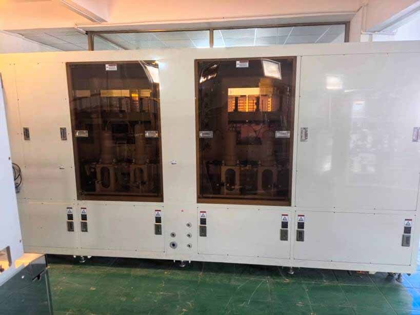

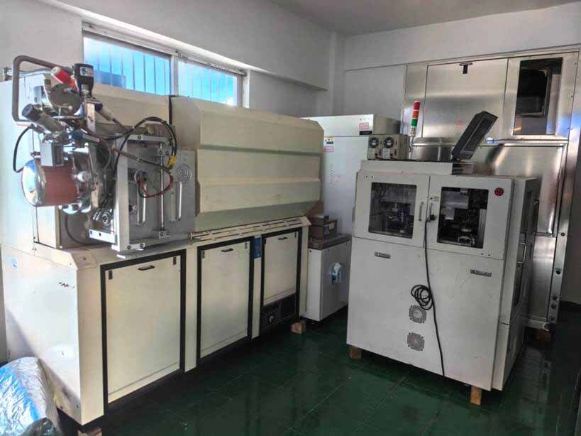
FAIRCHILD CBA-M-2000 is an advanced photoresist equipment that offers precise and efficient photolithography capabilities for semiconductor manufacturing processes. This state-of-the-art equipment is designed to produce high-quality patterns on substrates through a series of photolithographic steps, essential for creating integrated circuits and other microelectronic devices. CBA-M-2000 is manufactured by FAIRCHILD Semiconductor, a leading provider of semiconductor solutions. At the heart of FAIRCHILD CBA-M-2000 system is its sophisticated photoresist deposition and exposure capabilities. Photoresist is a light-sensitive material that undergoes chemical changes when exposed to ultraviolet light, allowing for the transfer of patterns onto substrates. CBA-M-2000 utilizes a programmable spin coating unit to evenly apply a thin layer of photoresist onto the substrate surface. This precise coating is essential for achieving uniformity and consistency in the subsequent patterning steps. One of the key features of FAIRCHILD CBA-M-2000 is its high-resolution exposure machine, which is capable of producing intricate patterns with sub-micron precision. The tool uses a high-intensity ultraviolet light source to selectively expose the photoresist-coated substrate, defining the desired patterns. The exposure process is controlled by advanced software algorithms that ensure accurate pattern transfer and alignment, crucial for achieving the desired device performance and functionality. CBA-M-2000 asset also offers advanced alignment and registration capabilities to ensure the precise overlay of multiple pattern layers. By using sophisticated alignment marks and alignment algorithms, the model can achieve sub-micron registration accuracy, essential for creating complex multi-layer devices with tight dimensional tolerances. This level of precision is critical for modern semiconductor manufacturing processes, where device densities continue to increase. In addition to its patterning capabilities, FAIRCHILD CBA-M-2000 equipment also incorporates advanced process monitoring and control features to optimize the performance and efficiency of the photolithography process. Real-time monitoring of key process parameters, such as photoresist thickness and exposure dose, allows for immediate feedback and adjustments to ensure consistent and reliable patterning results. This level of process control is essential for maximizing yield and minimizing defects in semiconductor production. Furthermore, CBA-M-2000 system is designed with scalability and flexibility in mind, enabling it to meet the evolving requirements of semiconductor manufacturers. The unit can accommodate a wide range of substrate sizes and types, allowing for versatility in various production environments. Additionally, the software interface of the machine is user-friendly and intuitive, making it easy to configure and operate the equipment for different patterning applications. Overall, FAIRCHILD CBA-M-2000 photoresist tool represents a cutting-edge solution for semiconductor photolithography, offering precision, efficiency, and reliability for the production of high-performance microelectronic devices. With its advanced features and capabilities, CBA-M-2000 is well-suited for semiconductor fabs and research institutions looking to push the boundaries of semiconductor technology and innovation.
There are no reviews yet