Used FSI / TEL / TOKYO ELECTRON 915597-005 #9360975 for sale
URL successfully copied!
Tap to zoom
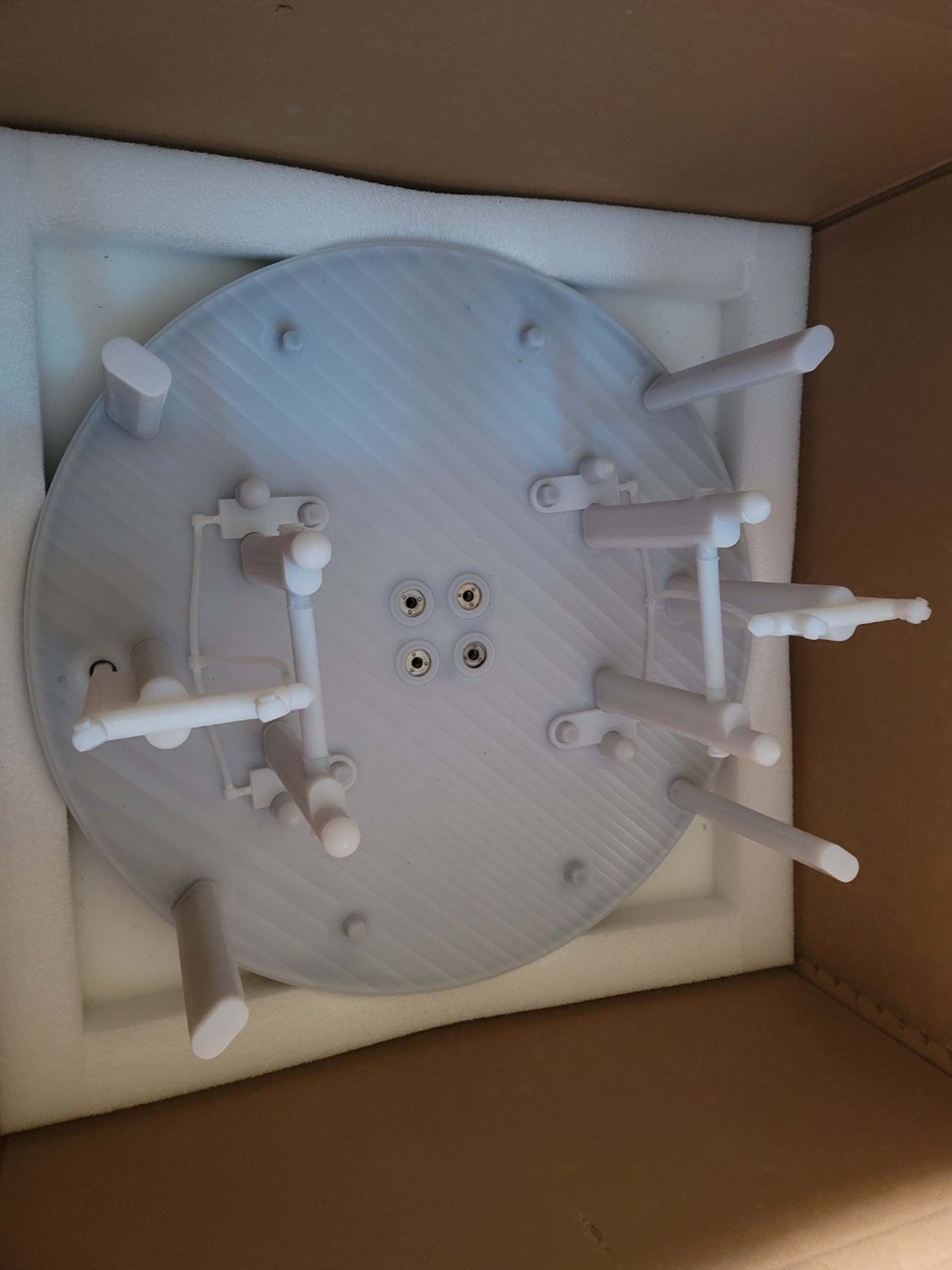


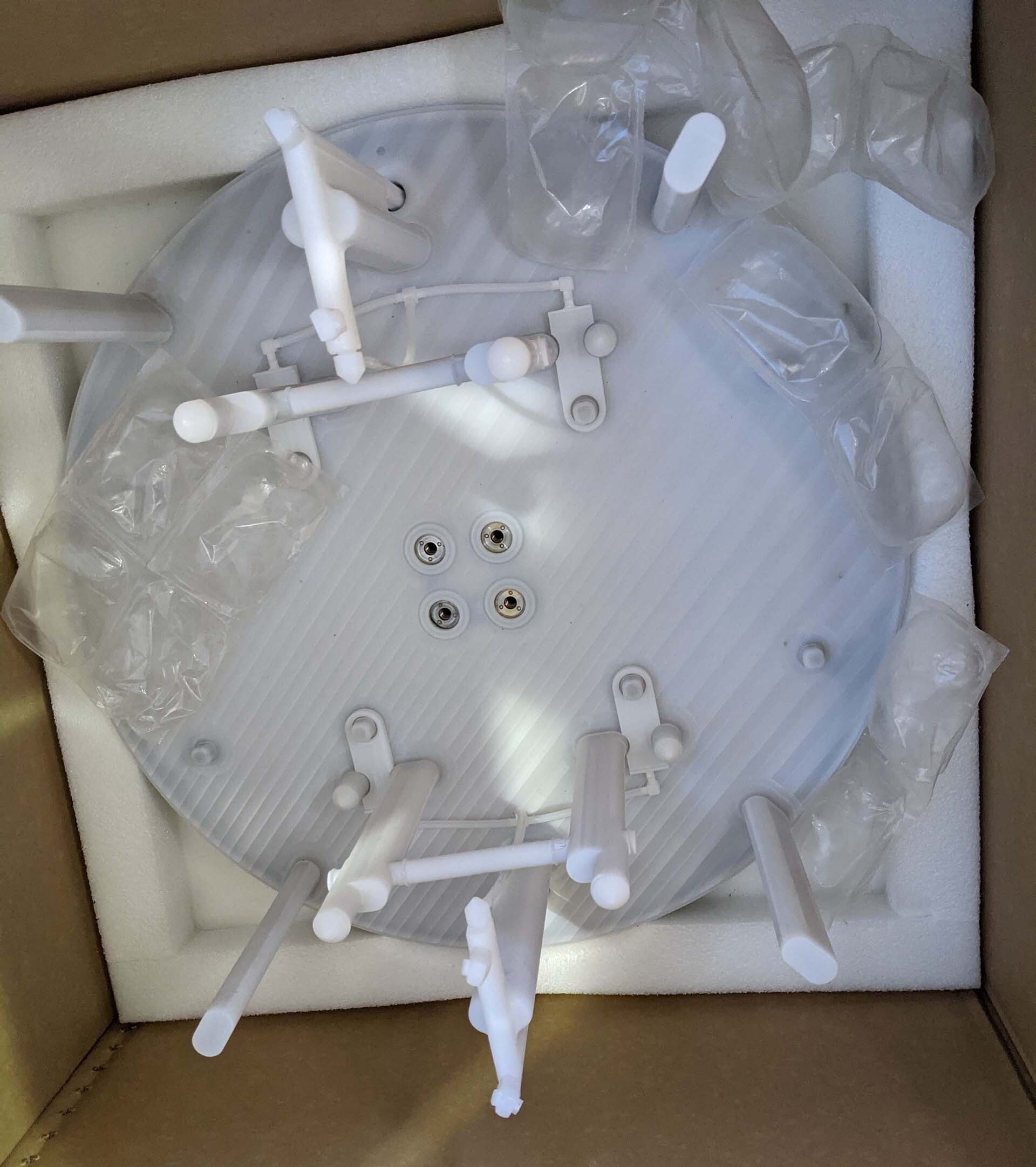

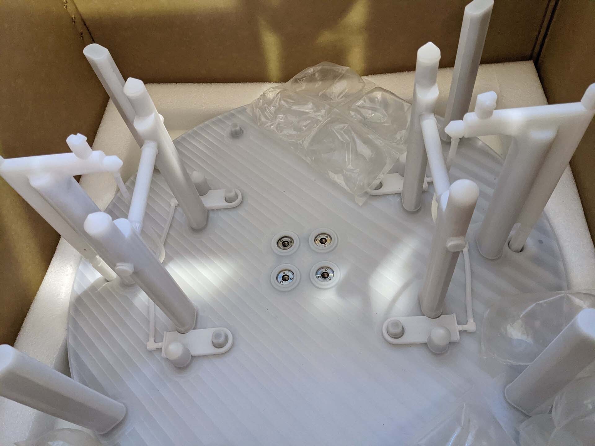

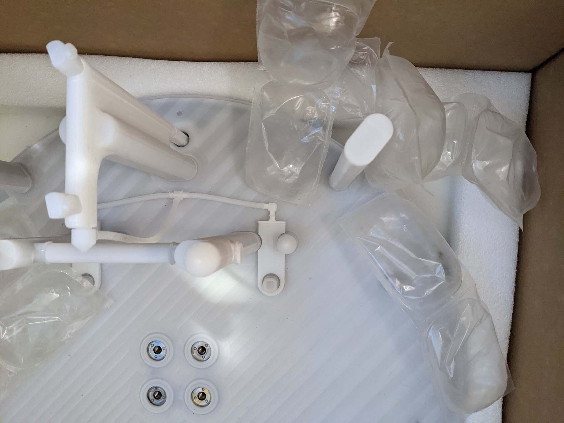

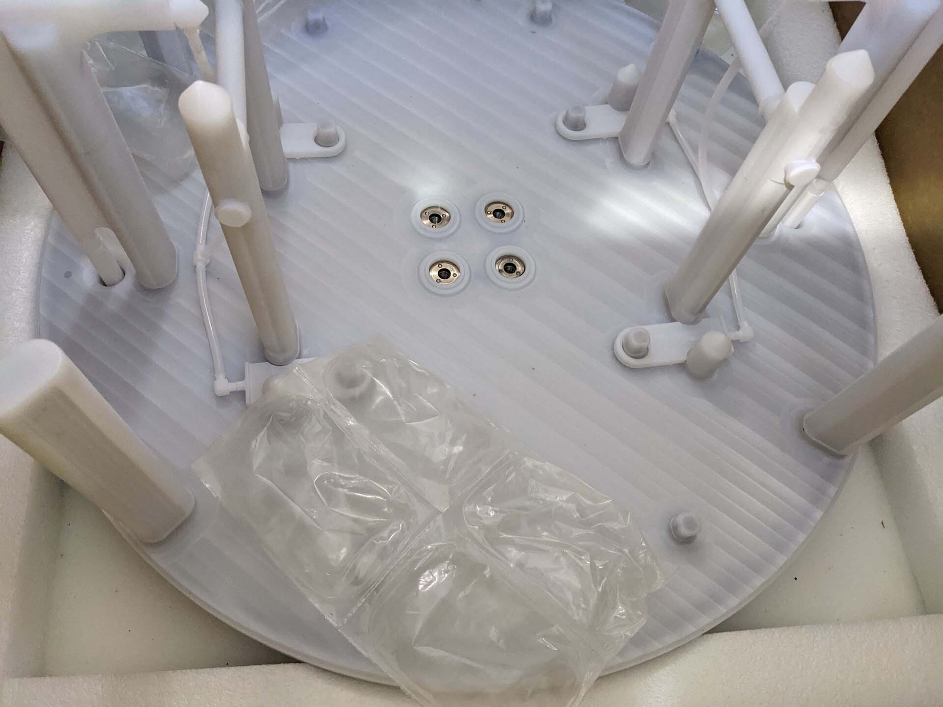

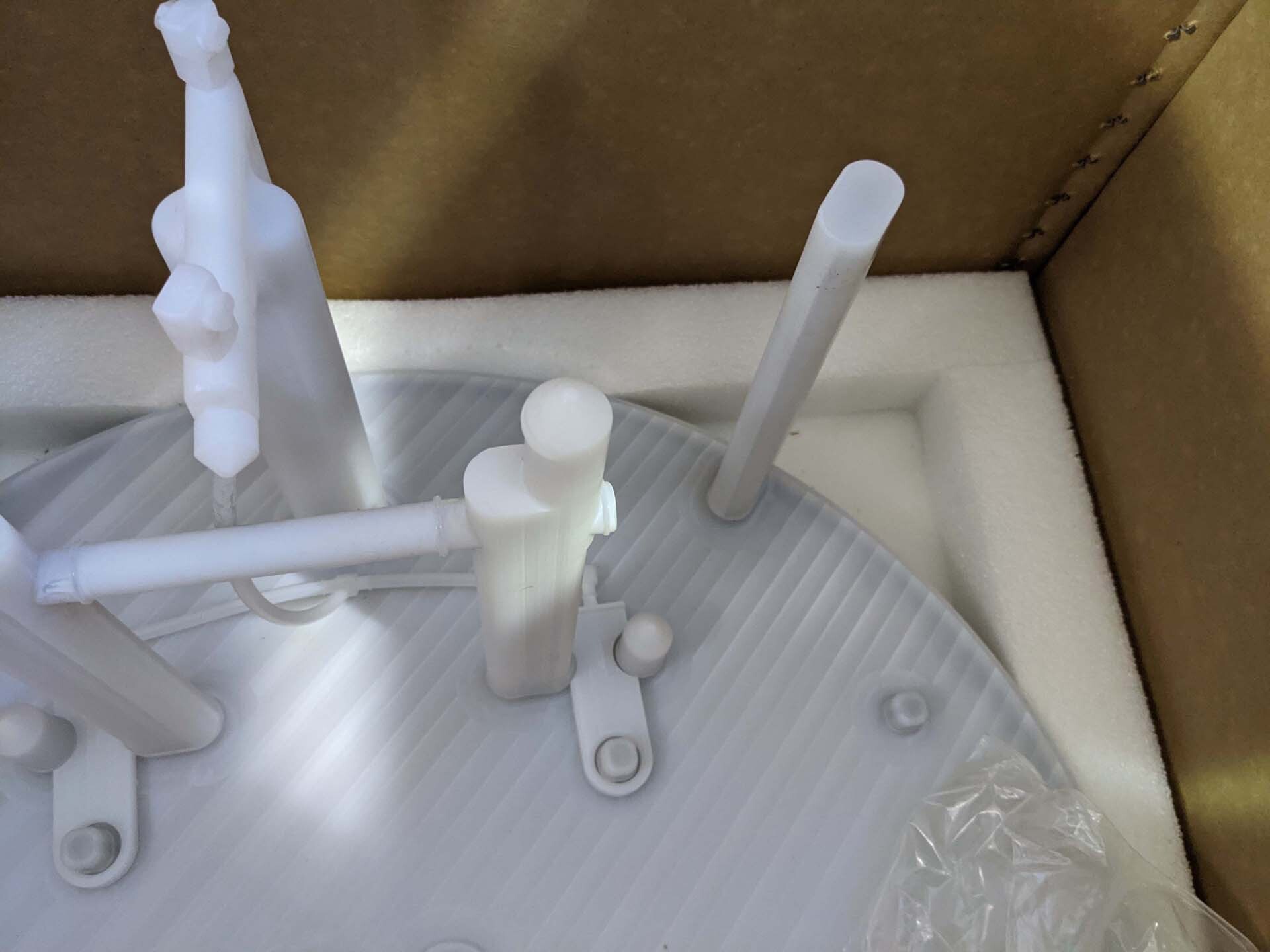

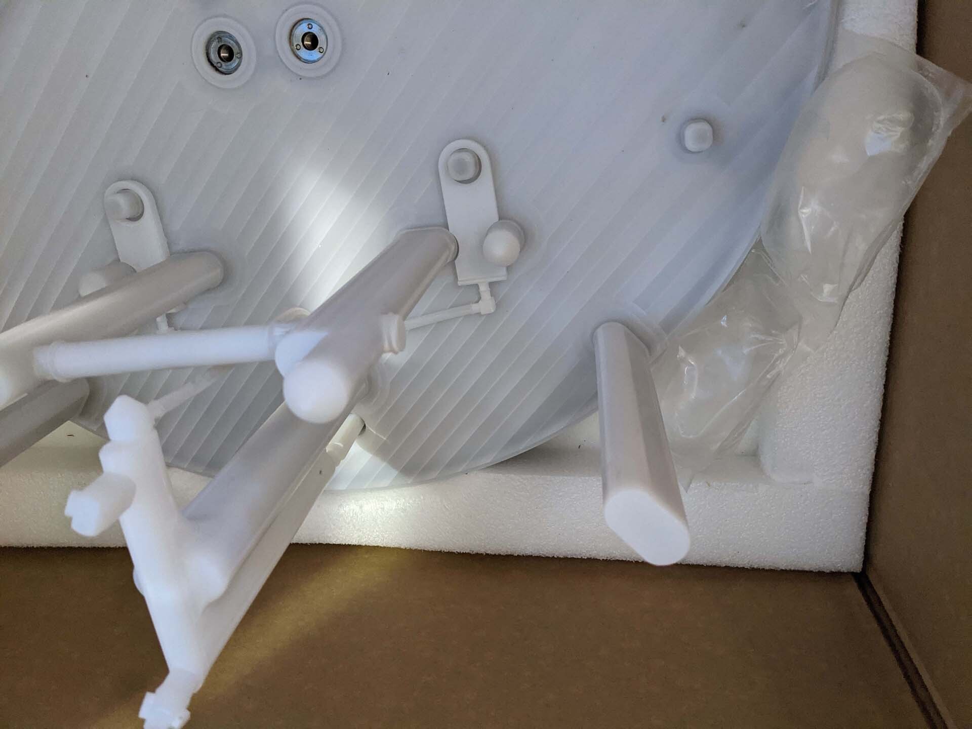


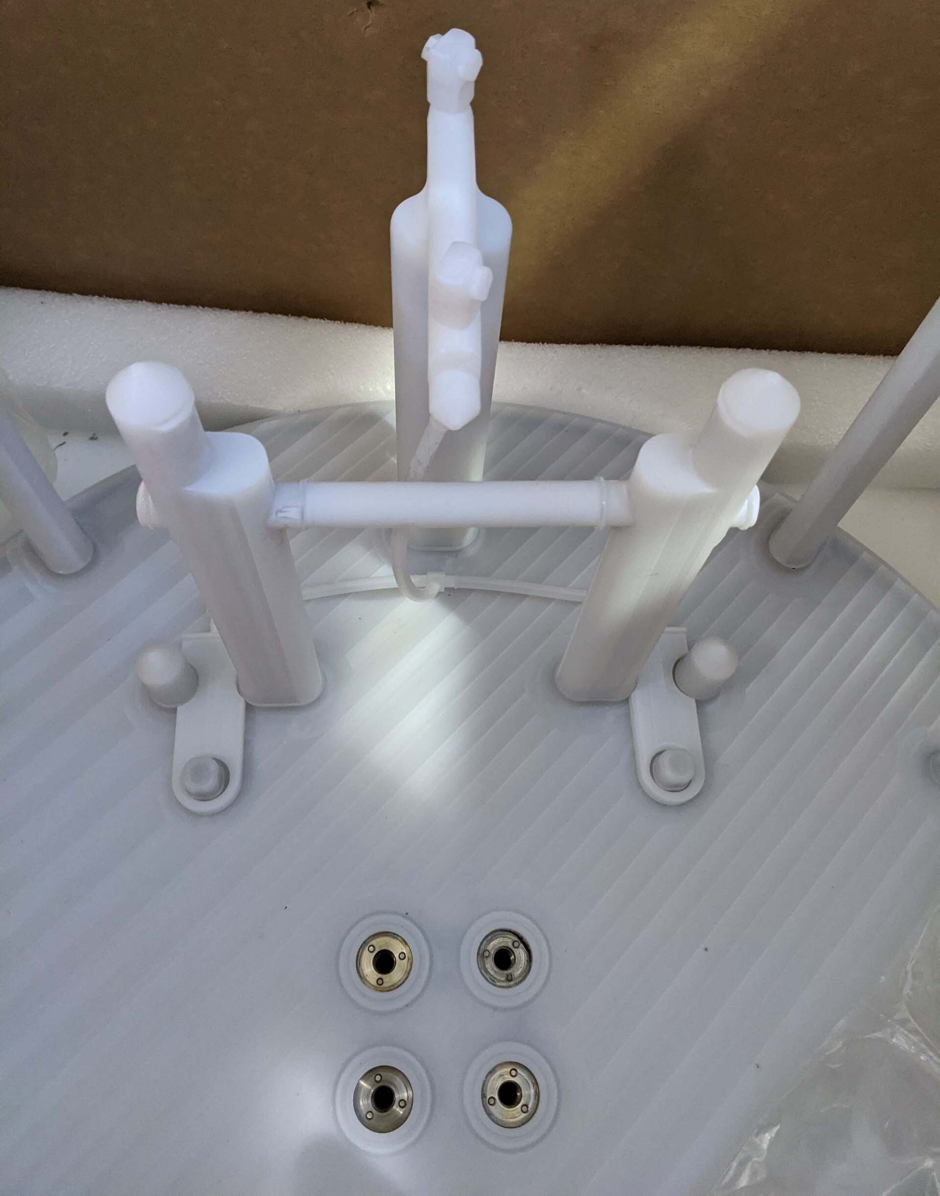

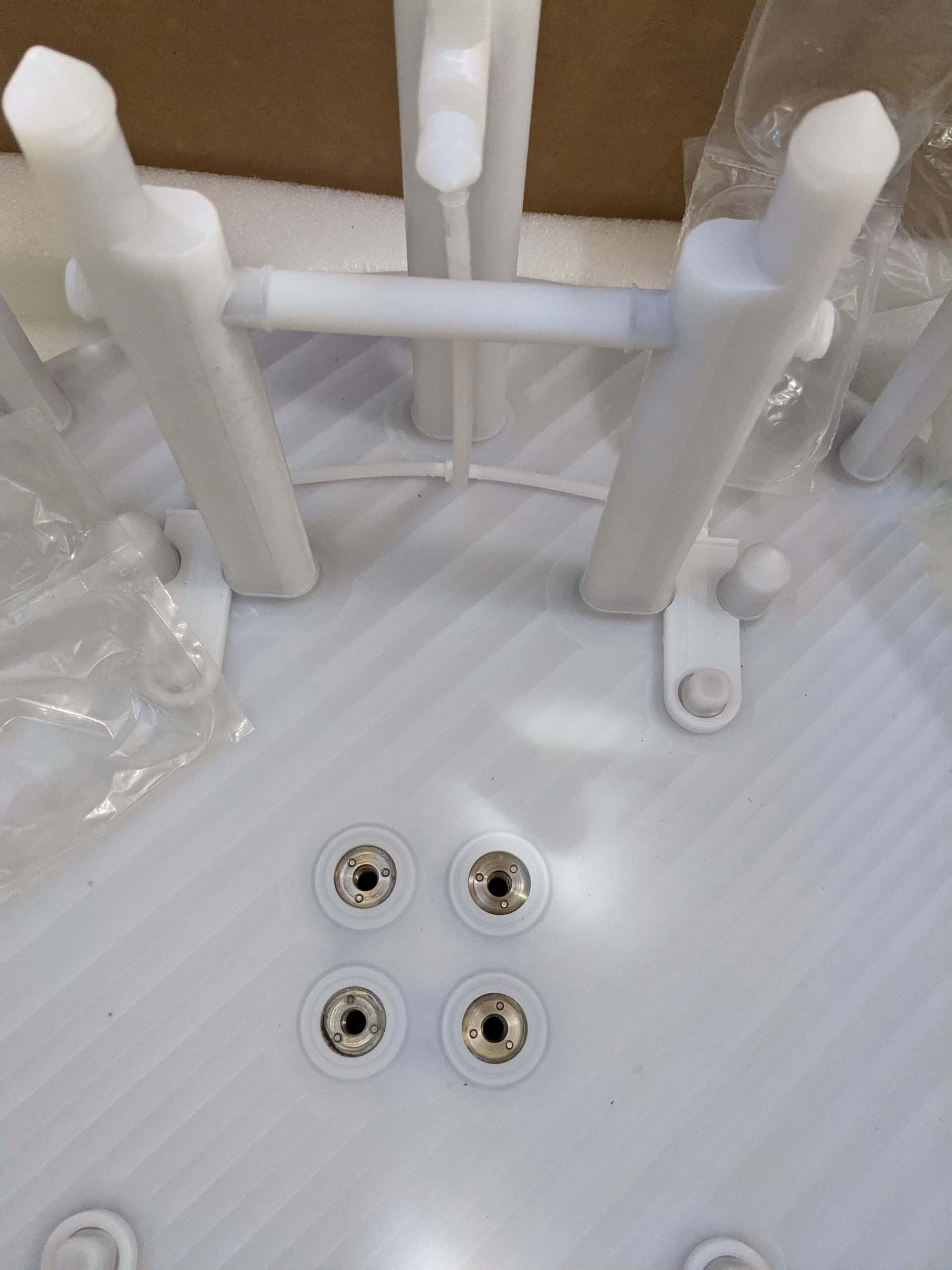



FSI / TEL / TOKYO ELECTRON 915597-005 photoresist equipment is a photolithography system that is designed to enable the production of very complex microstructures on semiconductor wafers and other substrates. The unit is designed to provide fast, precise, and repeatable imaging of patterns across a wide range of mask sizes. It offers exposure speeds up to five frames-per-second, the highest resolution of any photolithography machine available, and precise exposure control. The tool includes a 4-inch stepper photomask that is designed to provide patterns for accurate and repeatable imaging on substrates up to 6 inches in size. It features a highly sensitive film that is able to accurately capture the patterns from the mask, resulting in improved exposure results and highly repeatable patterns. The asset also features an integrated film feeder and processing model that allows for easy setup and clean-up between exposures. The equipment also includes a thorough set of imaging tools to customize the performance of the system. These tools include automatic shutter control, automatic alignment and focus control, and programmable wafer handler software. Additionally, the unit includes exposure control software which allows users to easily adjust and customize the exposure parameters and monitor the results during imaging. Finally, the machine includes an array of imaging optics that provide enhanced imaging of substrates of a variety of sizes and configurations. This includes variable focal length lenses, depending on the size of the substrate and the resolution of the pattern. The imaging optics can also be customized to provide special effects for more complex patterning, such as variable depth imaging, halftone imaging, and higher contrast imaging. Overall, FSI 915597-005 photoresist tool is an excellent choice for high resolution, repeatable, and versatile imaging and processing of semiconductor wafers and other substrates. Its high precision exposure control, imaging tools, and state-of-the-art optics, allow for flexibility and customization when producing complex microstructures.
There are no reviews yet

