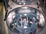
Used FSI / TEL / TOKYO ELECTRON Atlas #57163 for sale
URL successfully copied!
Tap to zoom
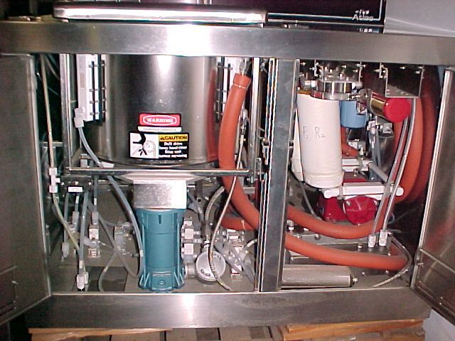


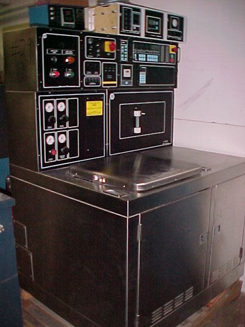

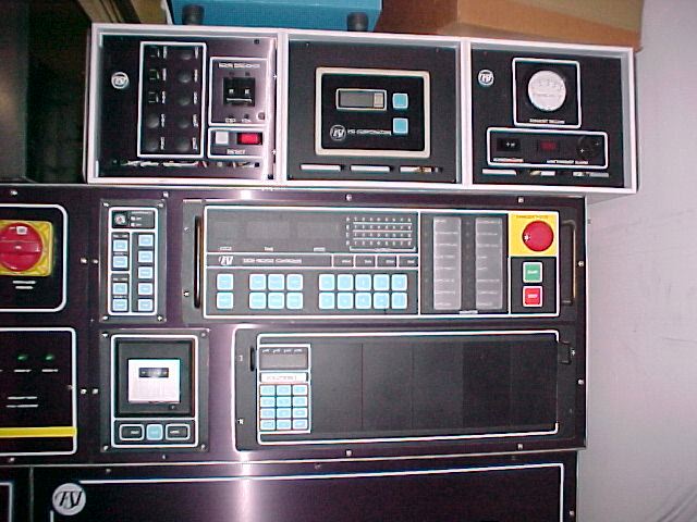


ID: 57163
Wafer Size: Up to 6"
Solvent processor, up to 6" with 2800 controller, RS232C and ss canister console with manual, 120 Volts.
FSI / TEL / TOKYO ELECTRON Atlas is a next-generation photoresist equipment designed to create nanoscale patterns on semiconductor wafers. It offers a comprehensive set of functionalities for process control, with capabilities for both post-imaging and pre-processing activities. The system is equipped with a high-end photo imaging tool which exposes light to the photoresist layer to create patterns on the semiconductor wafer. It functions at wavelengths between 360 nm to 800 nm, and can be adjusted to match the characteristics of different resists and photo processes. The photo image tool is capable of achieving sub 0.2 μm resolution. The unit also contains a wafer stage that features active stabilization, a key feature to achieve the desired nanoscale accuracy. The wafer stage supports a range of wafer sizes and thicknesses, and is capable of rapid iterative processes like laser mask writing. FSI Atlas comes equipped with a high speed robot that is able to perform process steps at high throughput. It includes microprocessing headers which can be used to precisely modify the pattern on the wafer. It also features a high-end resist management capability which ensures clean and stable development of the resist layer. This also allows remote monitoring of process parameters, helping ensure quick resolution of process issues. The machine also comes with a highly-efficient chemical management technology which can be used to precisely control the coating and developing of the photoresist. This chemical management tool helps to reduce the number of defective chips produced. Additionally, the asset is integrated with a manufacturing execution model which can be used to monitor the entire resist process over the long-term. Overall, TEL Atlas is an advanced photoresist equipment designed for high-precision nanoscale manufacturing of semiconductor wafers. It offers powerful functionalities for both pre-processing and post-imaging processes, allowing users to create and modify patterns safely and reliably.
There are no reviews yet
