Used FSI / TEL / TOKYO ELECTRON K150 #293624501 for sale
URL successfully copied!
Tap to zoom
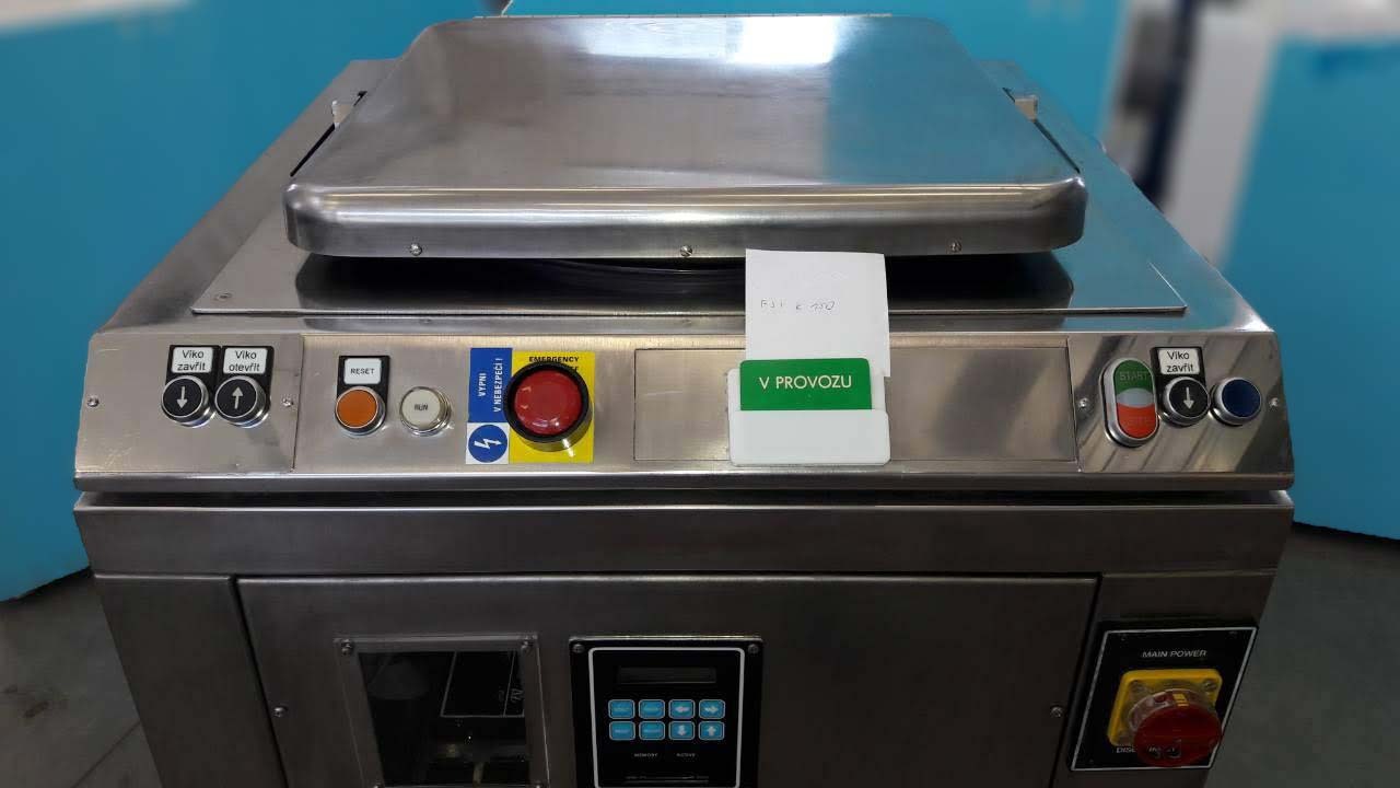

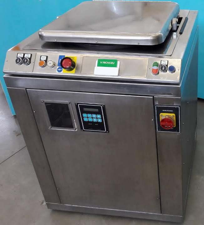

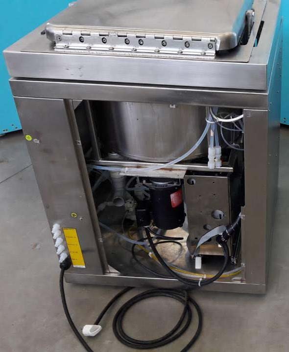

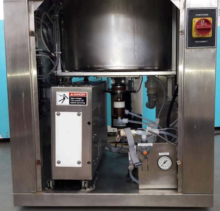

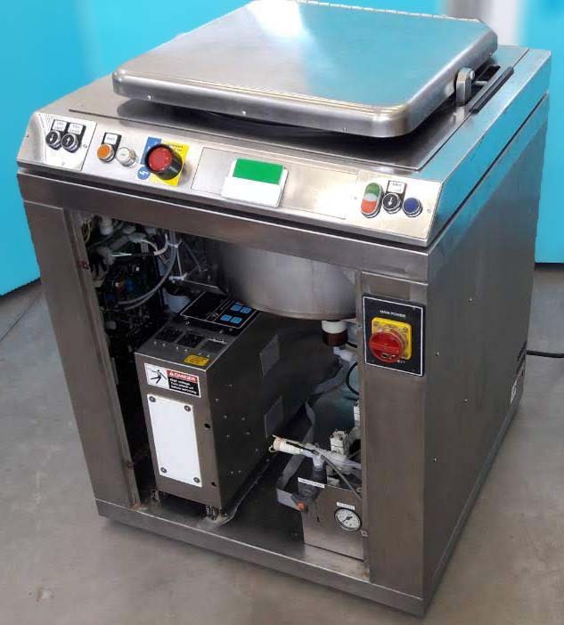


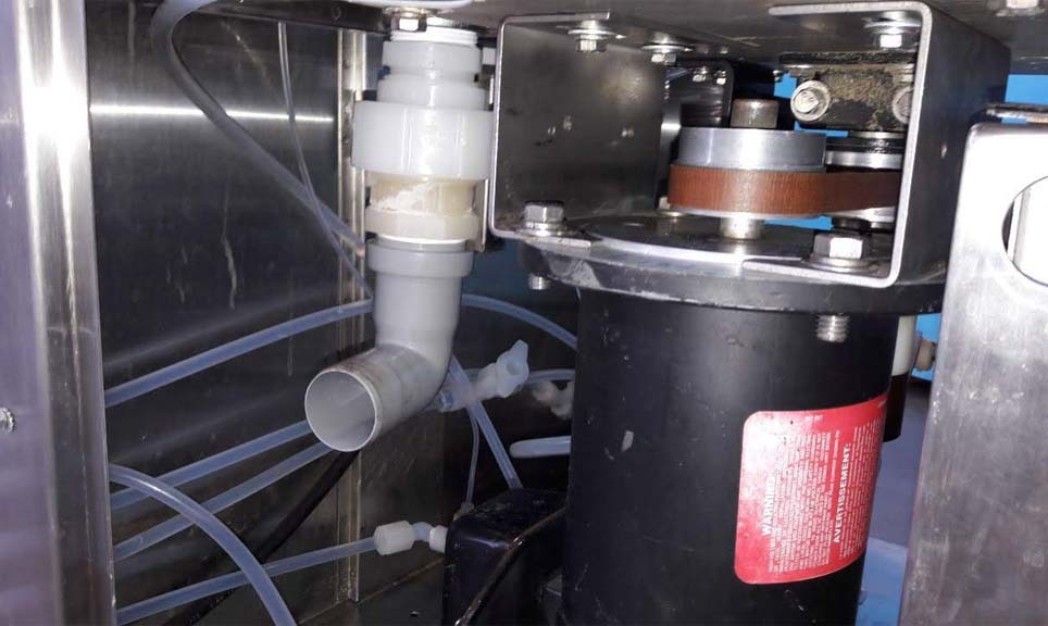

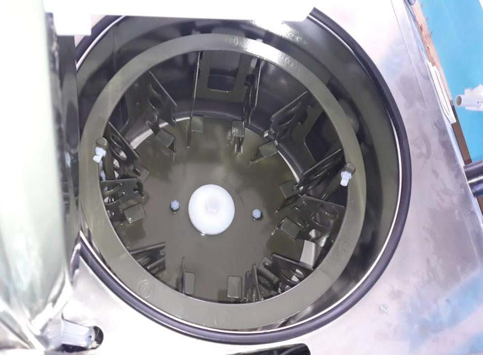


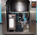
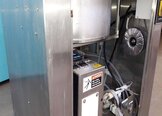
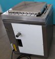
FSI / TEL / TOKYO ELECTRON K150 Photoresist Equipment is an automated device designed for high-precision photolithography processes in semiconductor production. It is used to physically pattern various layers of thin substrates in ultrafine detail, with a wide variety of materials such as quartz, silicon, and polyimide. The system employs 4 optical stages, a precision scanning stage and a high-power laser unit to accurately and precisely pattern an exact feature. The first optical stage is equipped with a Canon 20x microscope and a 5-camera photocard machine for precise monitoring and measurements. This stage also provides alignment checks for all imaging components. The second optical stage, mounted on a robotic arm, contains a zoom lens along with a patterning mirror to ensure accurate imaging. A long focal length objective lens is mounted on the third optical stage, providing a magnified view of the substrate and allowing recording of even the smallest details. Finally, the fourth optical stage houses a high-power UV light source, a cast base plate to support the substrate, and a variety of positioners and actuators to precisely direct the laser beam. The control tool of FSI K150 Photoresist Asset is responsible for the automated imaging process, and includes a built-in multimedia sub-model and advanced sensors for advanced inspection and measurement. The equipment is also able to work with a variety of communication protocols, allowing for easy integration with external equipments. A user-friendly graphical interface permits the user to configure the system, set up parameters and specifications, and monitor the unit's performance. TEL K150 Photoresist Machine also includes a self-diagnostic routine which can detect and report any malfunctions, enabling immediate corrective action if necessary. The tool is capable of patterning features ranging from 0.1 to 1 micron in size, with an accuracy of +/- 5 nm and resolution of 1-10 nm. Its high-grade components and mechanisms assure long-term durability and consistent operation. K150 Photoresist Asset's high-quality imaging tools, precise and controlled processes, and superior automation make it an ideal solution for advanced and demanding photoresist jobs.
There are no reviews yet
