Used FSI / TEL / TOKYO ELECTRON Mercury #9030479 for sale
URL successfully copied!
Tap to zoom
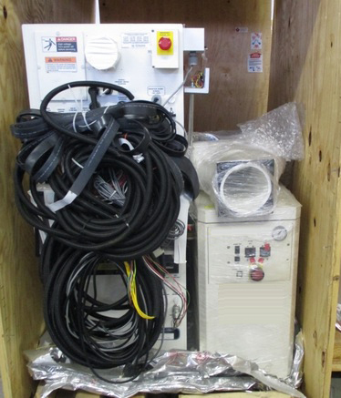


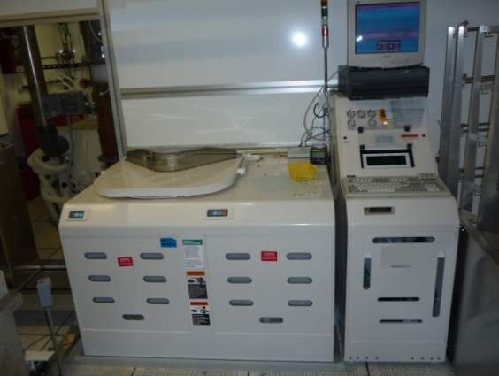

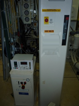

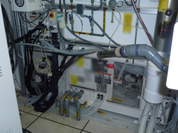

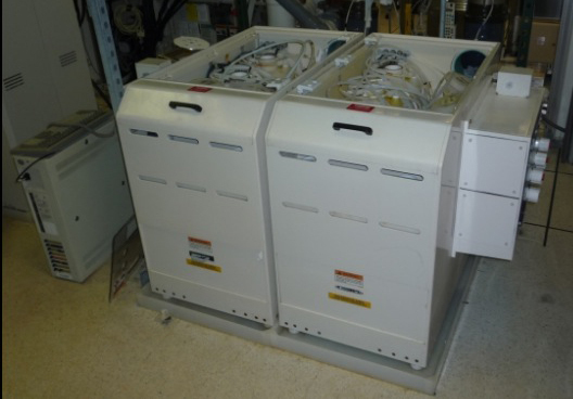

ID: 9030479
Wafer Size: 8"
Vintage: 1996
Metal etch system, 8"
De-installed
1996 vintage.
FSI / TEL / TOKYO ELECTRON Mercury is a photoresist equipment designed to accurately expose UV and Visible light onto semiconductors and other materials with high precision. It features a highly reliable ultraviolet exposure system with excellent consistency that can be used for various substrates. It also has laser alignment functions, in addition to a movable stage for accurate patterning and intensifying/scattering. FSI Mercury uses High Precision Spin Coater, which enables precise and uniform coating of photoresists on the substrate. This unit incorporates special features, such as a controller for variable spin speed and temperature control - for example, for the substrate heating prior to spinning. The wafer stage paired with the spin coater has a capacity for 200mm wafers. TEL Mercury's DUV (Deep Ultraviolet) light source is specifically designed to achieve high levels of exposure accuracy and offers a wide range of features, including an optical density adjustment machine for uniform exposure. Its positioning tool ensures that the exposure targets are accurately aligned for the most effective results. Mercury's light source also has a shutter function, designed to reduce crosstalk between the exposure systems. Together with the CCD Image Sensor at the bottom of the asset, this ensures that a clear and repeatable exposure is achieved. The 3-axis controller and the auto-leveling table further provide a stable basis for exposure without experiencing wobbliness. In addition, TOKYO ELECTRON Mercury has a sensitive and precise control model for scanning and patterning. It allows for fast patterning in both size and shape, allowing for the efficient and accurate production of on-chip patterns. Overall, FSI / TEL / TOKYO ELECTRON Mercury is a valuable and effective photoresist equipment for photolithography and scanning processes. It enables precise and reliable pattern exposure, with superior control and wide range of features. This system is a reliable tool for delivering high quality results and is ideal for semiconductor and photomask fabrication.
There are no reviews yet

