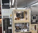
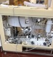
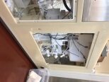
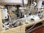
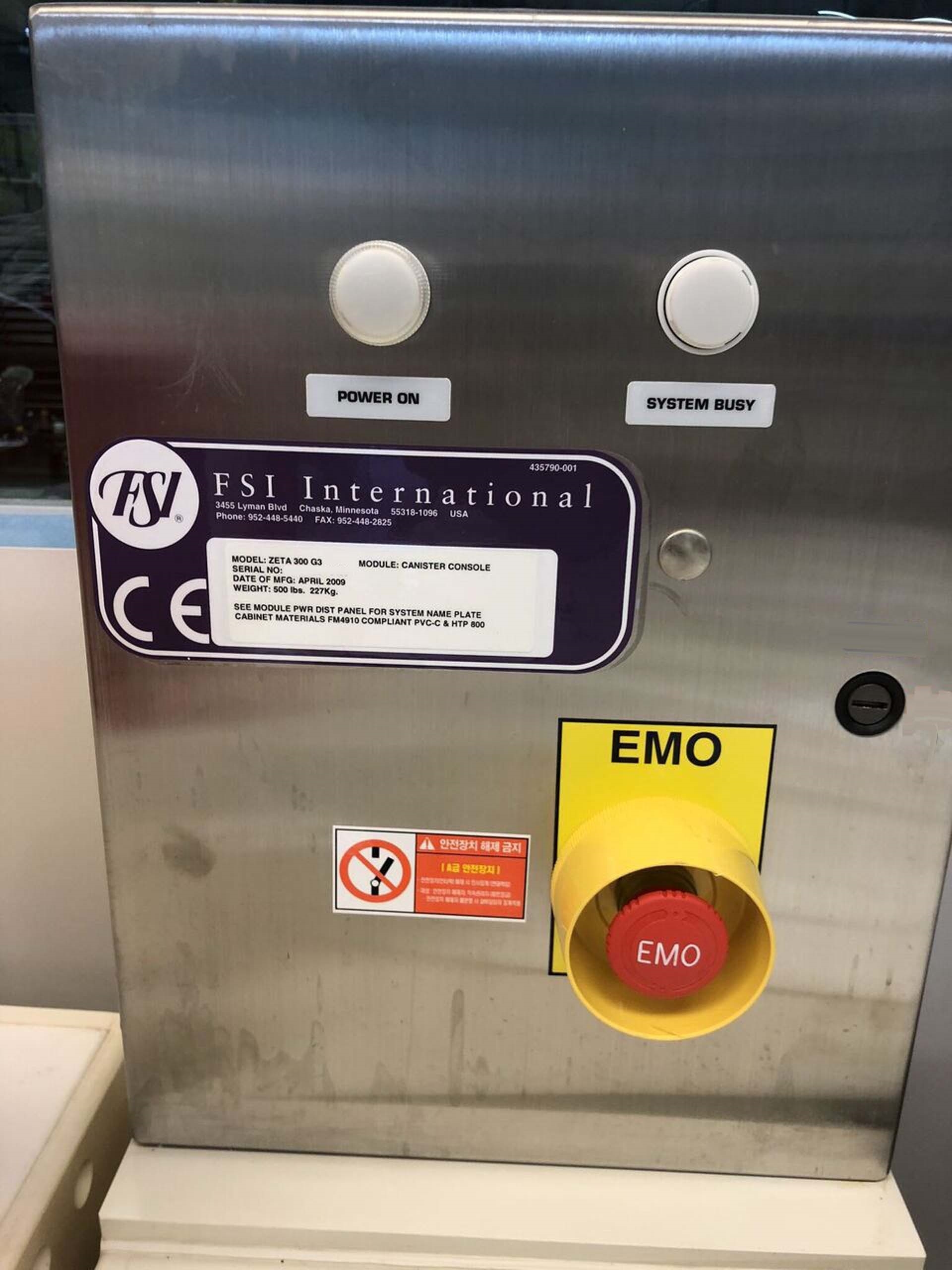
Used FSI / TEL / TOKYO ELECTRON Zeta 300 G3 #9181244 for sale
URL successfully copied!
Tap to zoom
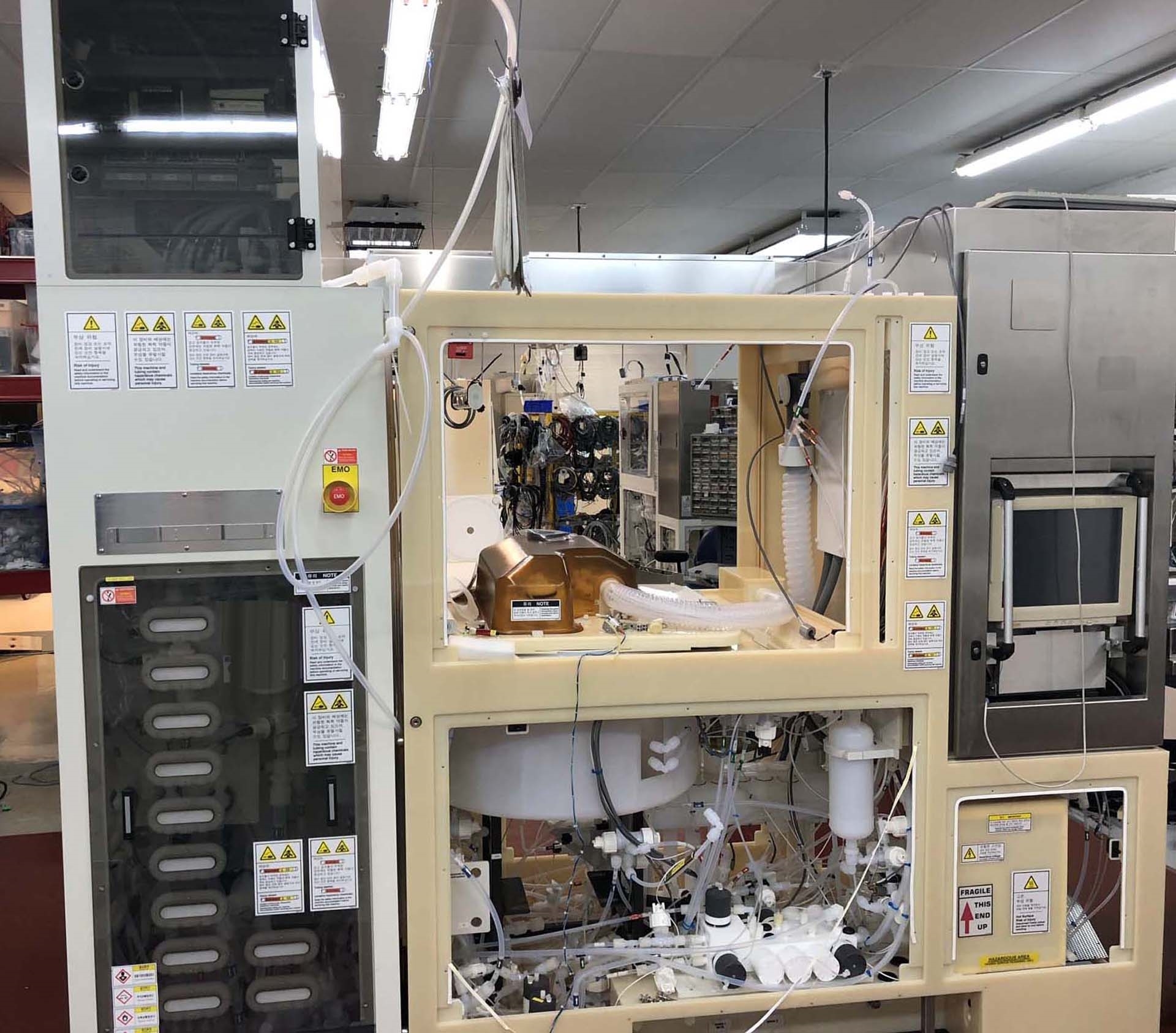

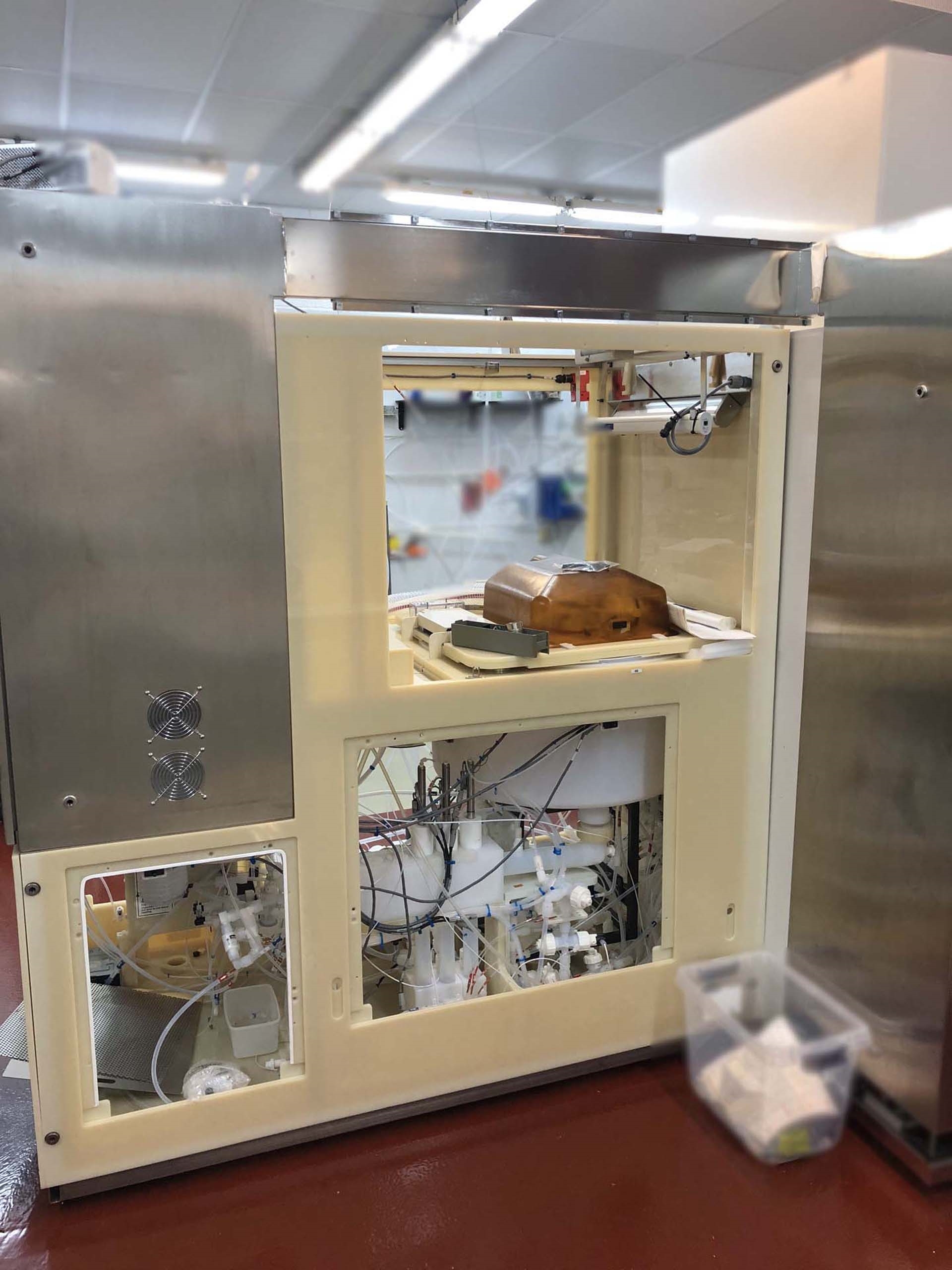


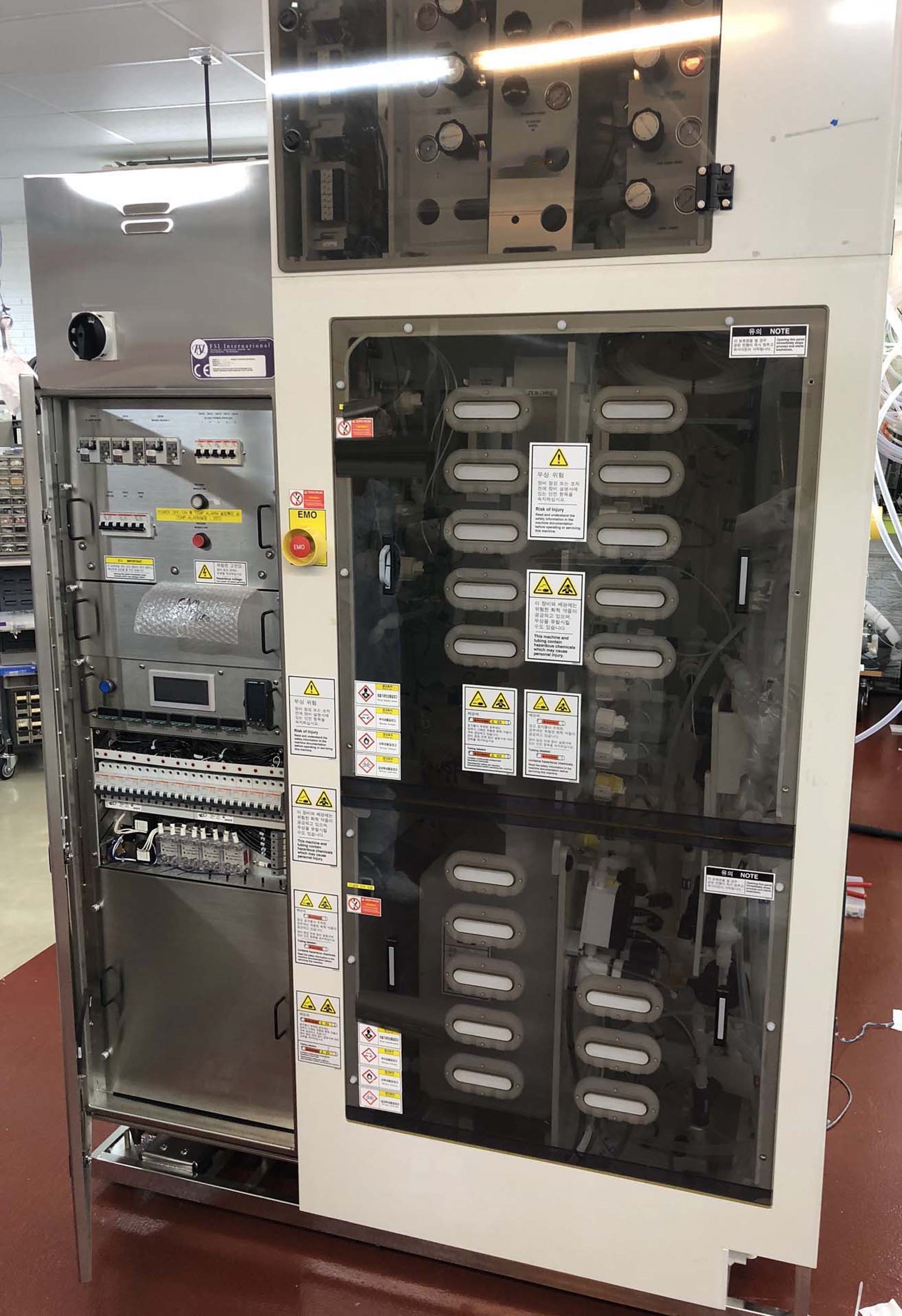

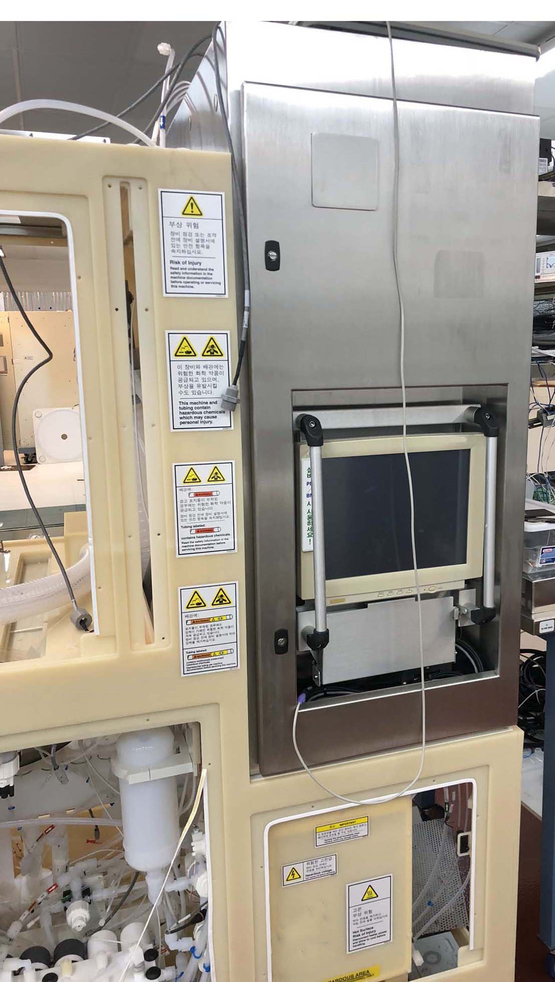

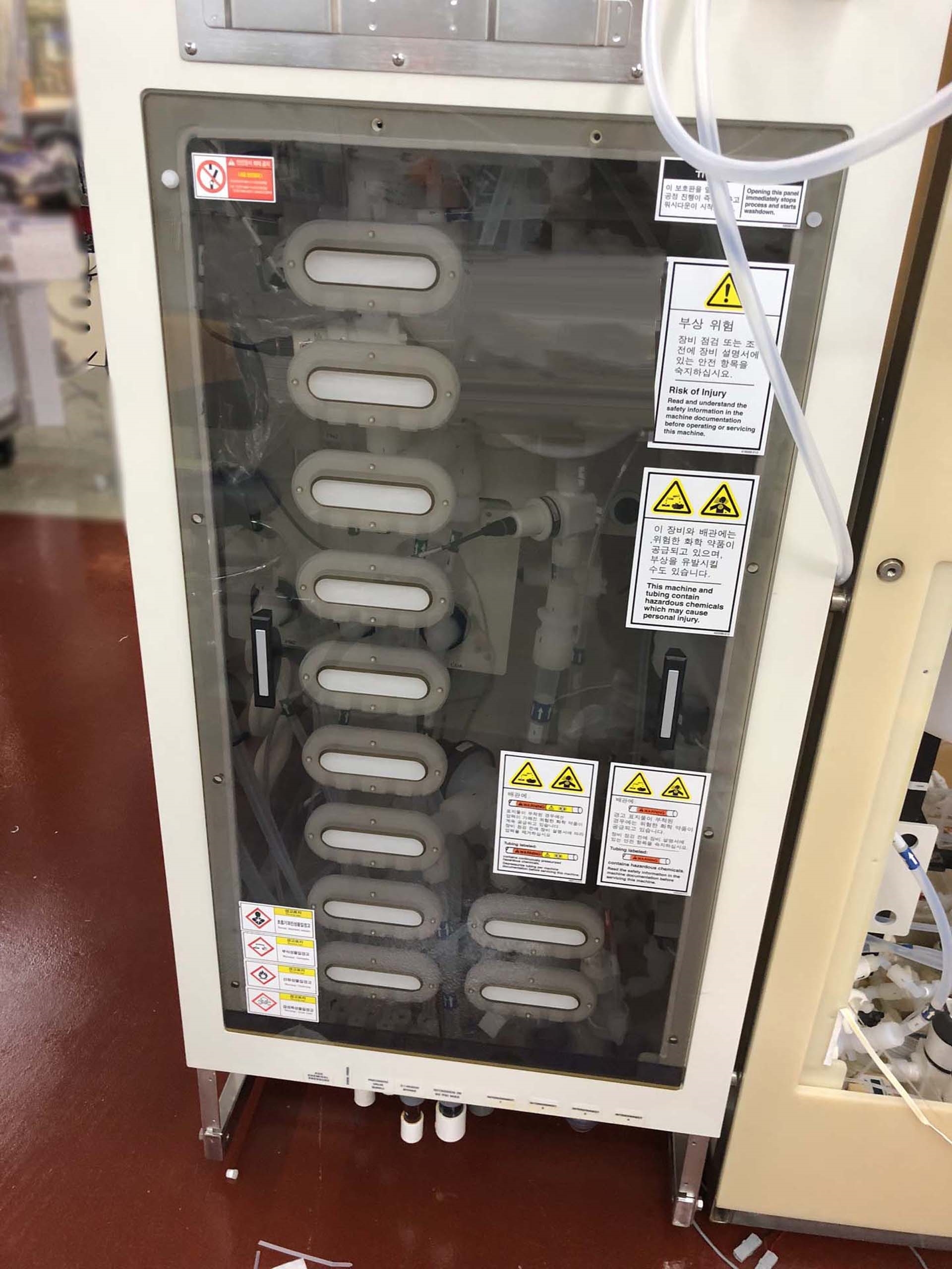

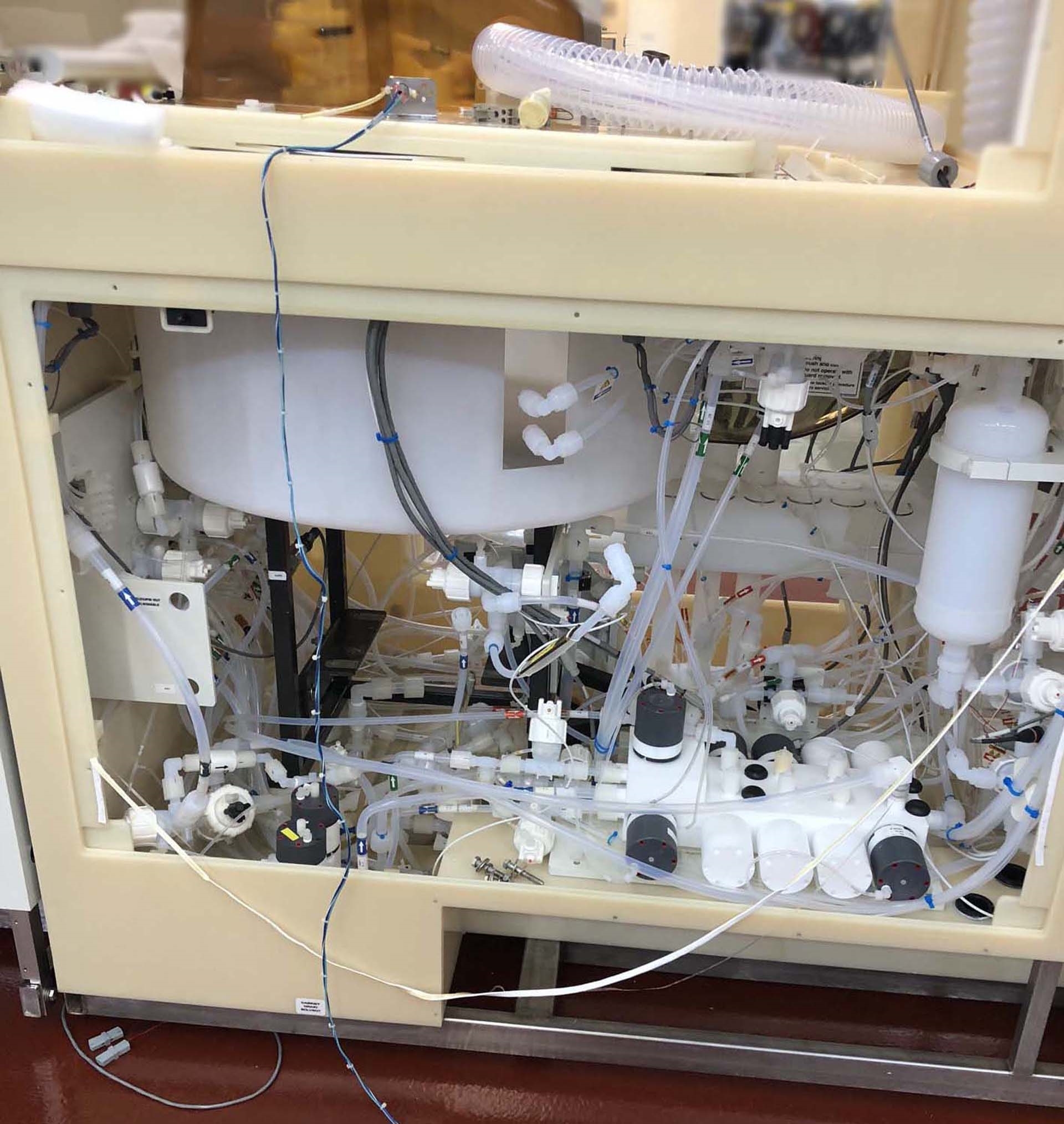










ID: 9181244
Wafer Size: 12"
Spray cleaning systems, 12"
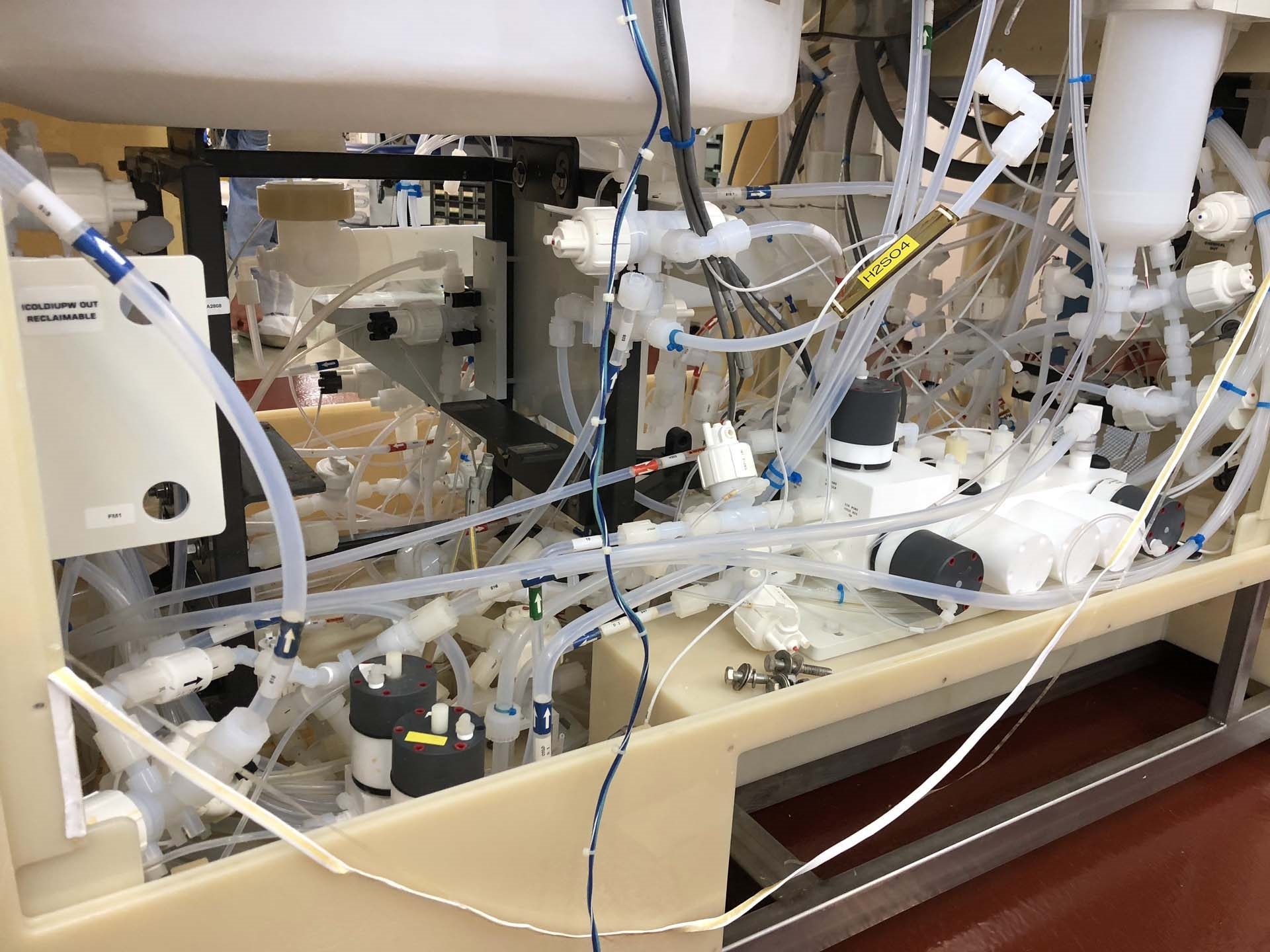
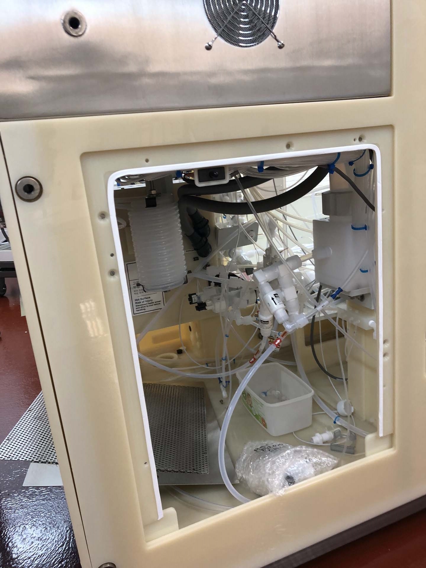
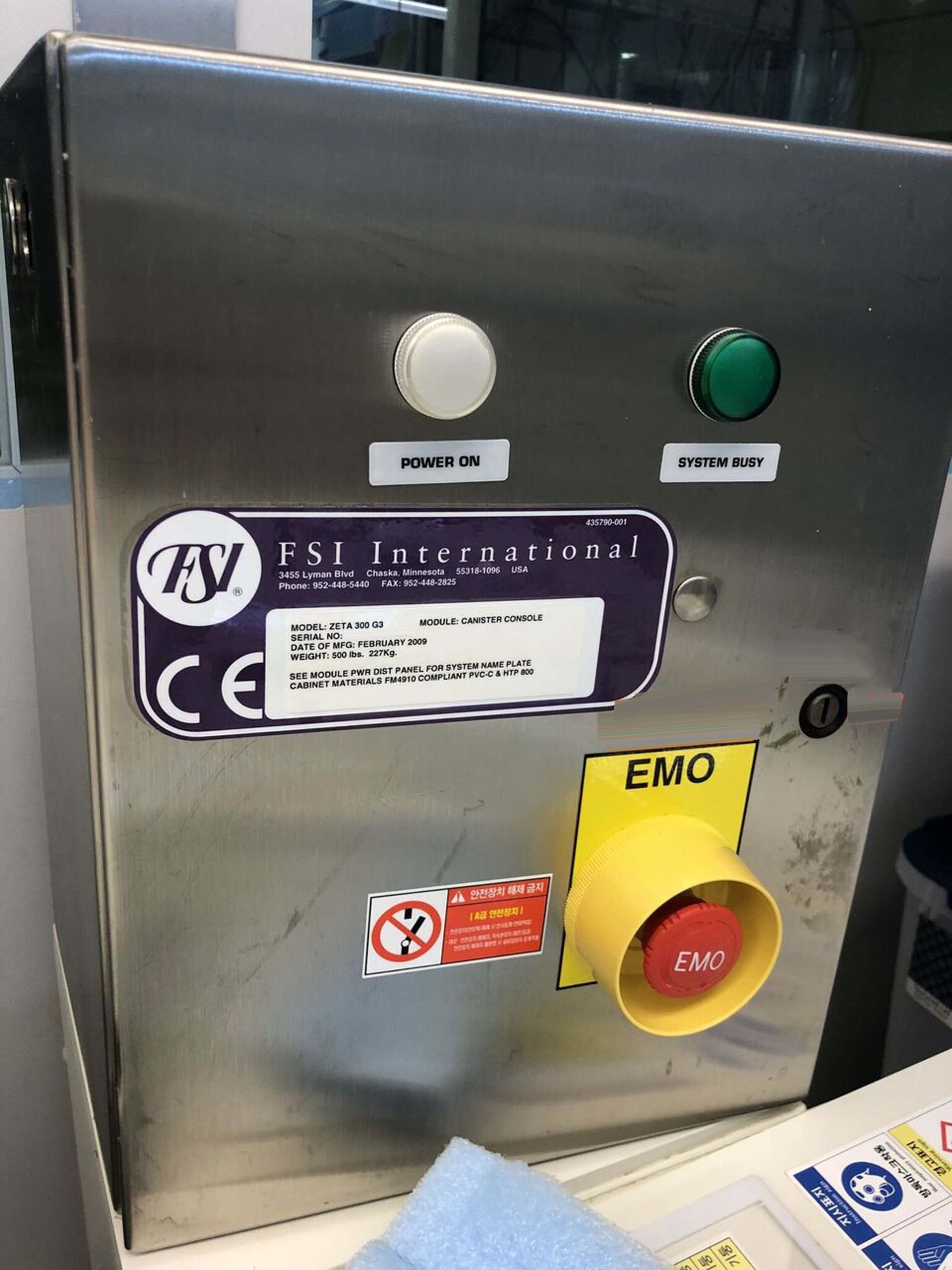
Canister consoles:
(6) Canisters, PTFE neck, No DVs
(2) 4-Position PVC-C consoles
Burst element caps
H2S04 Aspirator kit, 1/4"
(6) MYKROLIS Filters, QCDZ30P3F
(2) Chemical samplings / Shutoff boxes
MYKROLIS Filter WDFVATX2F
(2) CC Drip-trays
(5) 3/8" and (1) 1/2" CC Tubing, 10m
MHM:
STABULI TX90cr Cassette handler
Powder coated facade assembly
(4) PFA/Ti Wafer carriers, 12", 25-slots
(4) ASYST Load ports
0.07 Micron PTFE ULPA filters
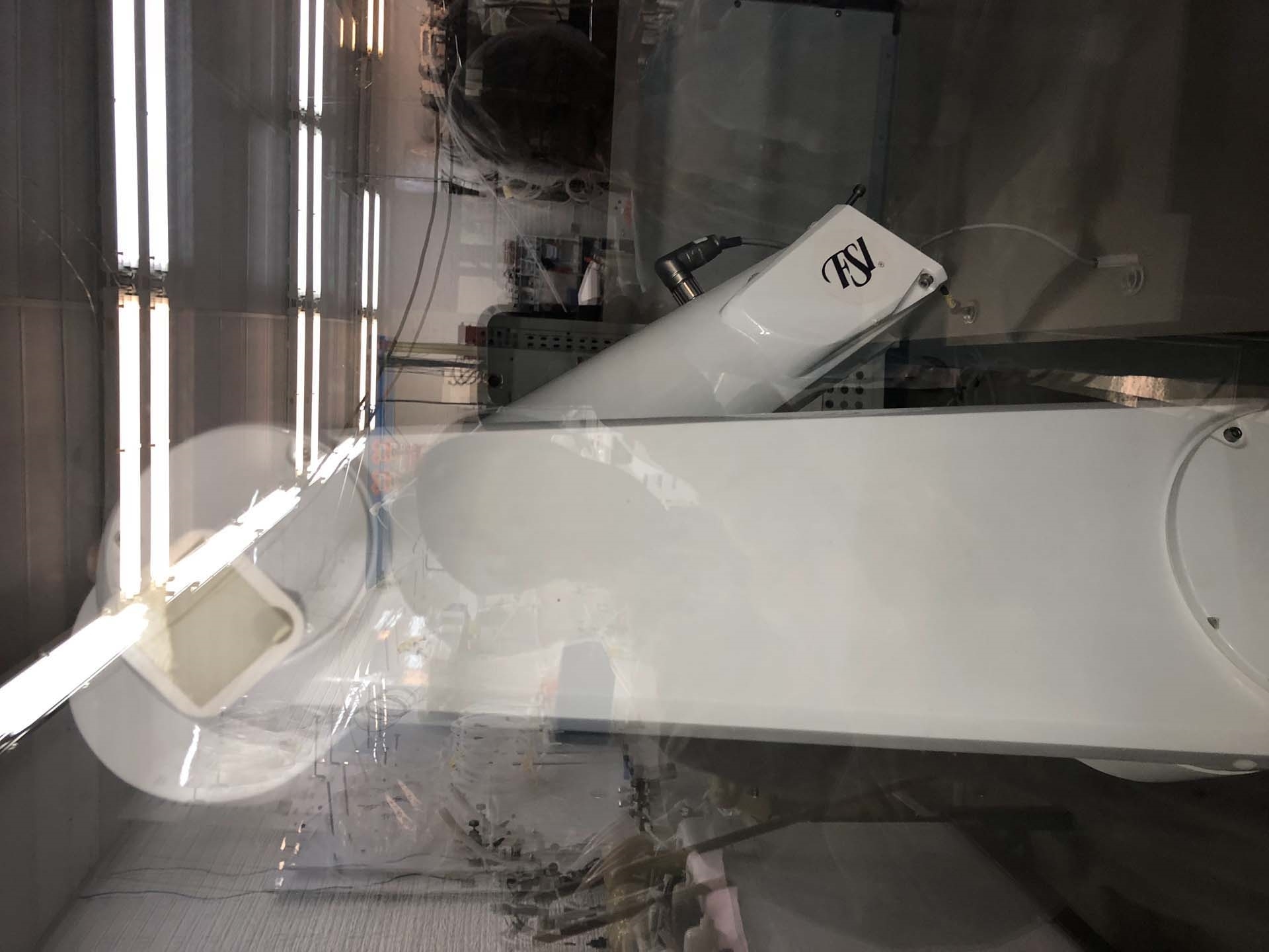
BROOKS Wafer handler and controller
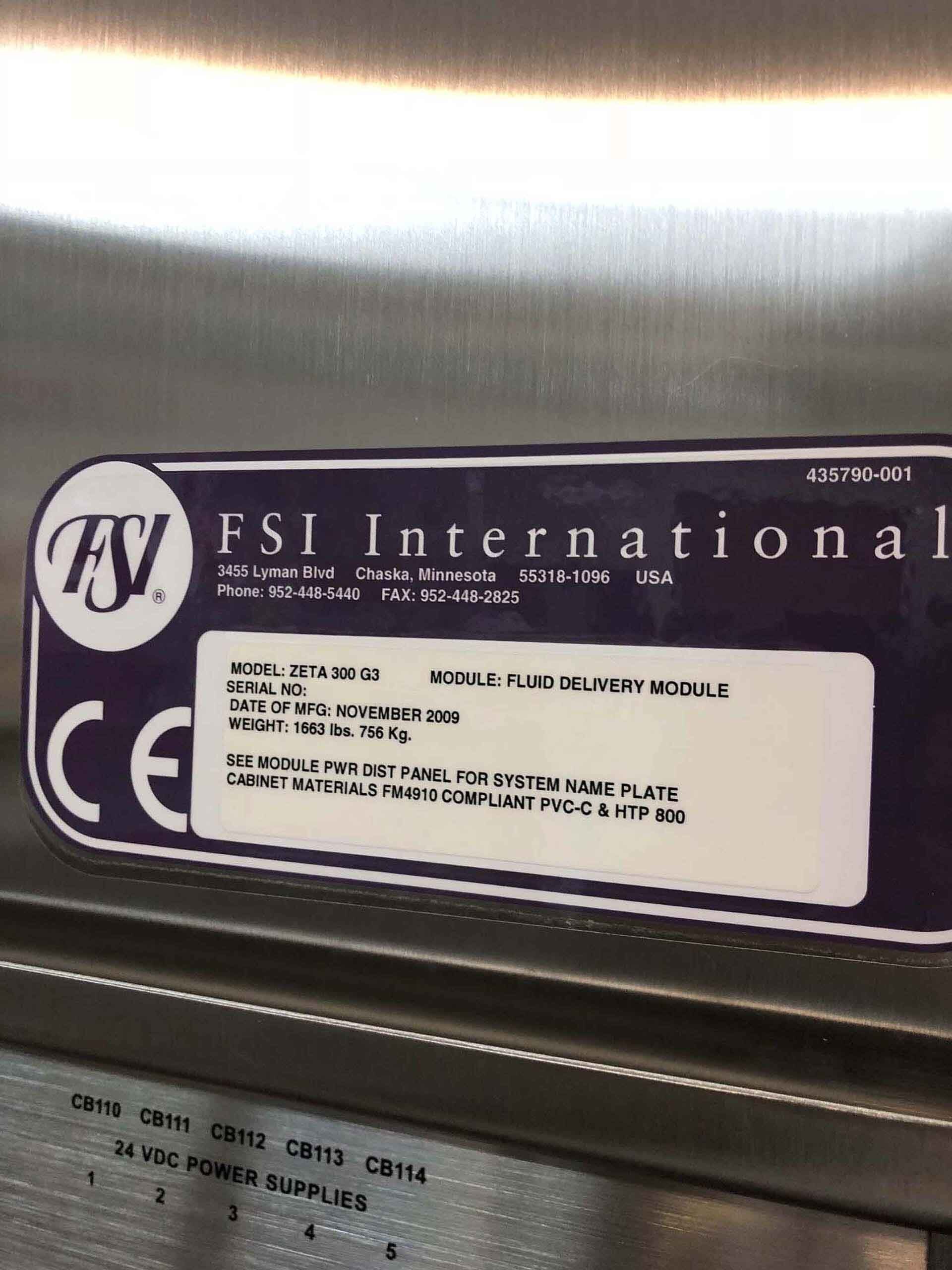
Fluid delivery module (PVC-C):
(5) 30-300cc Flow meters and operators
500-900cc Flow meter and operator
TREBOR 480V, 60kW Quartz DI heater
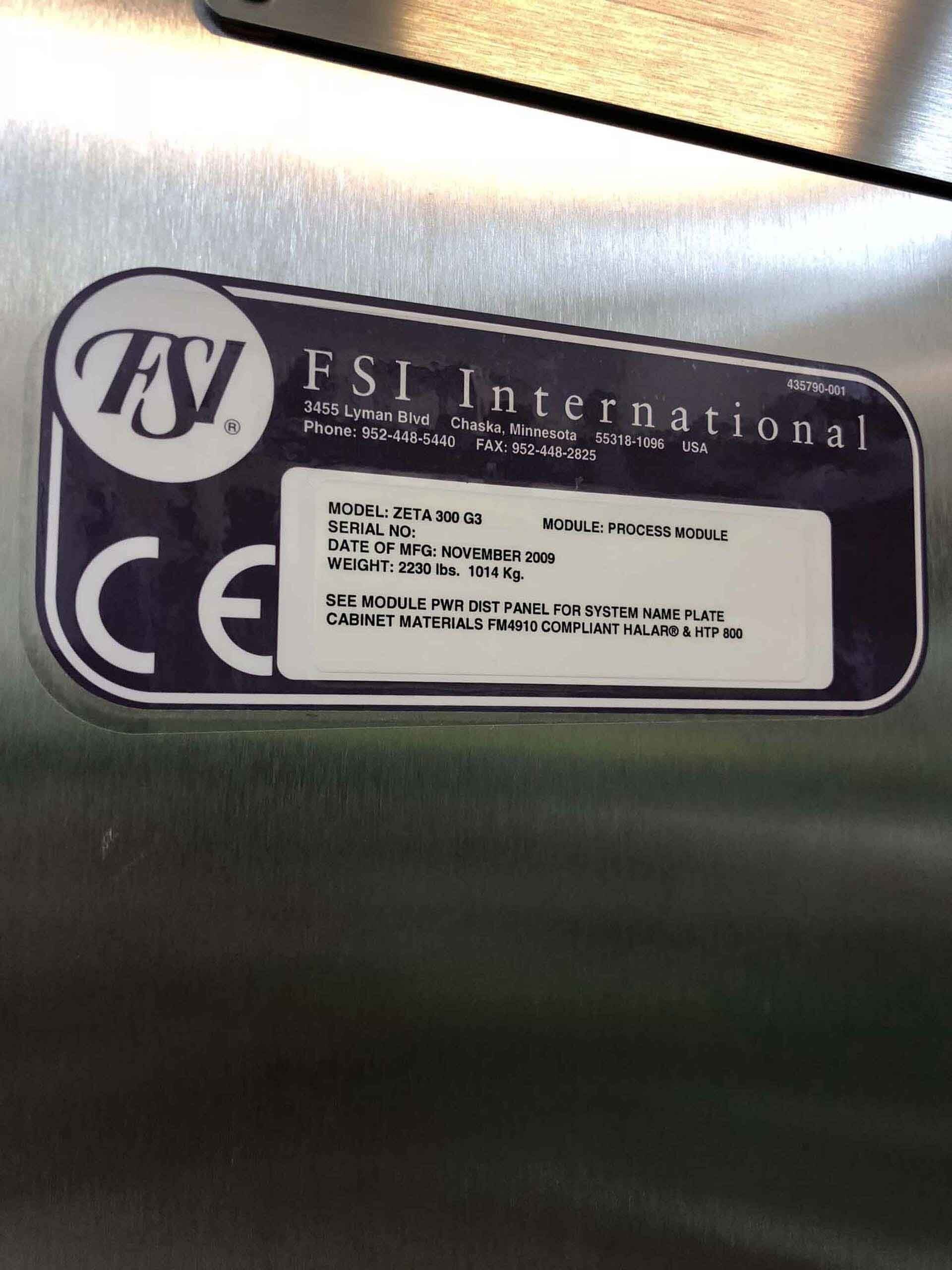
Process module:
HALAR cabinet
5-Port side bowl spray posts
(3) PTFE Drain valves
(3) PFA P-Traps
2-Position 12" PFA turntable
6-Valve chemical mixing block
Turntable hoist assy
Hot and cold rotary union
(2) Processes and cabinet exhaust damper
IR Heater with bypass
ViPR Hardware included
Operation and maintenance manuals
Digital versions
2008-2009 vintage.
FSI / TEL / TOKYO ELECTRON Zeta 300 G3 is a photoresist equipment designed for precision and repeatable lithography for applications requiring fine detail in microelectronic, biomedical and optical fabrication. This system is equipped with advanced lithography capabilities such as stepper, scanning and flip chip alignment functions, and uses the latest electrolyte technology. FSI Zeta 300 G3 is an advanced i-line unit that enables the user to fabricate various pattern layouts with reduced process time and outstanding results. TEL Zeta 300 G3 photoresist machine combines high-speed imaging processed and unique advanced lithography technologies to deliver high-definition images without distortion. It offers an optimal imaging process and high resolution patterning capabilities which can produce small structures such as sub-100nm lines and spaces. It also features stepper, scanning and flip chip alignment functions for precise pattern placement on production substrates. TOKYO ELECTRON Zeta 300 G3 utilizes an electrolyte solution to remove contaminations from the resist film, and then applies the resist solution to the substrate surface. This ensures the highest level of distortion control and eliminates the need for multiple passes. A binder is also applied to the substrate surface to improve lithography results and reduce process times. The tool is also equipped with a variable focus lens that can adjust the focus to improve the resolution and contrast of images. In addition, Zeta 300 G3 is equipped with a source tuning section that allows the user to adjust the intensity and resolution of the exposure source. This feature enables the user to fine-tune the exposure dose without altering the resist processing conditions. Furthermore, FSI / TEL / TOKYO ELECTRON Zeta 300 G3 can be configured so that it can be automatically calibrated to a user's specific characteristics. Overall, FSI Zeta 300 G3 is a photoresist asset which has many advanced features, including stepper, scanning and flip chip alignment functions. It also has a unique electrolyte solution to ensure the highest level of distortion control, as well as a variable focus lens and source tuning section for maximum precision of images. As a result, TEL Zeta 300 G3 is the perfect tool for any microelectronic, biomedical or optical fabrication with a need for accurate patterning.
There are no reviews yet
