Used KARL SUSS / MICROTEC ACS 200 #9353323 for sale
URL successfully copied!
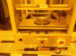
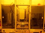
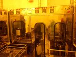




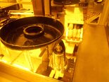

















Tap to zoom

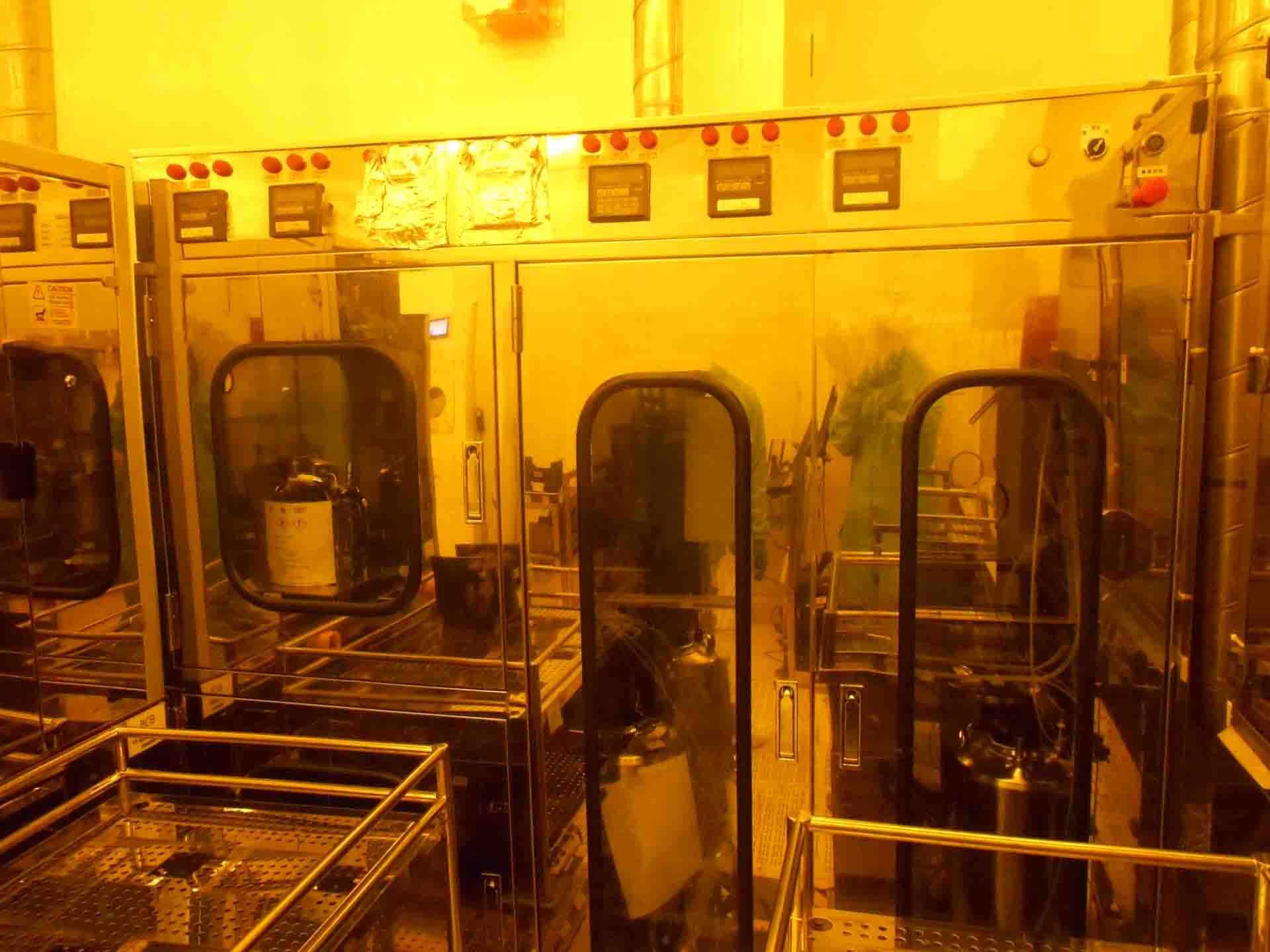
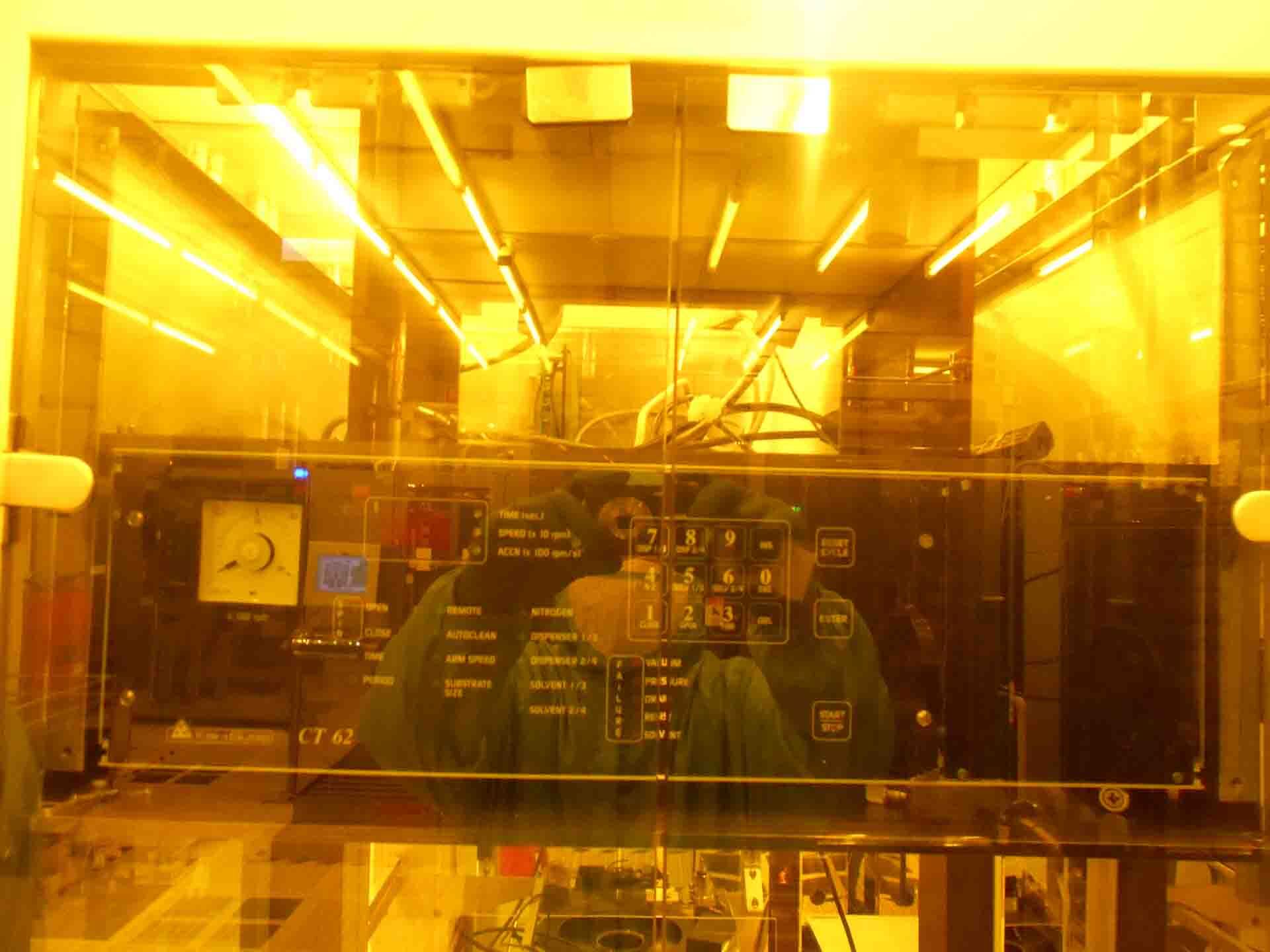
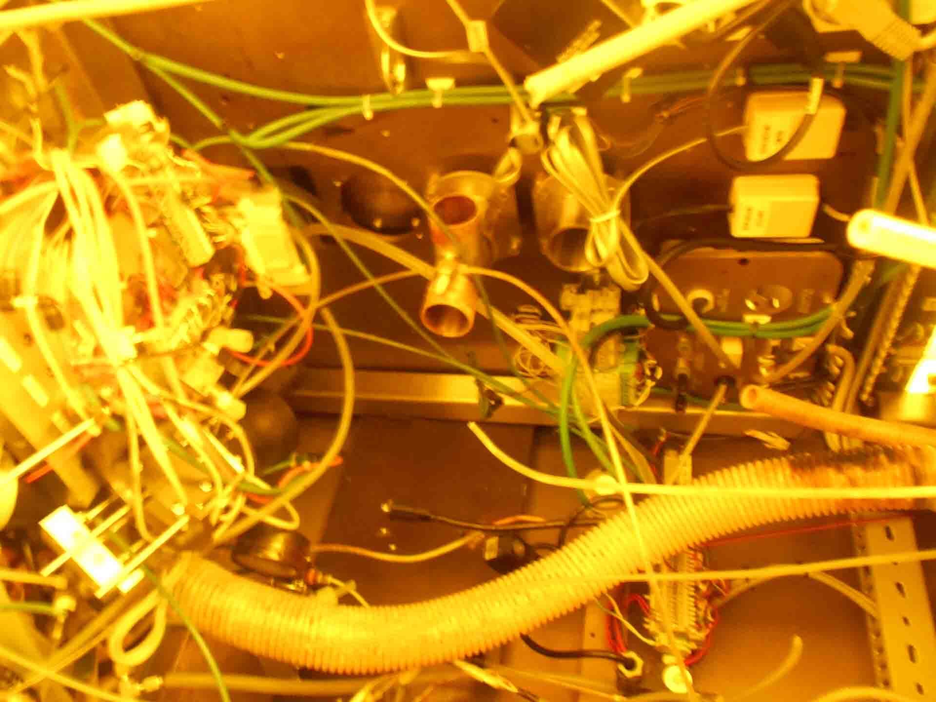
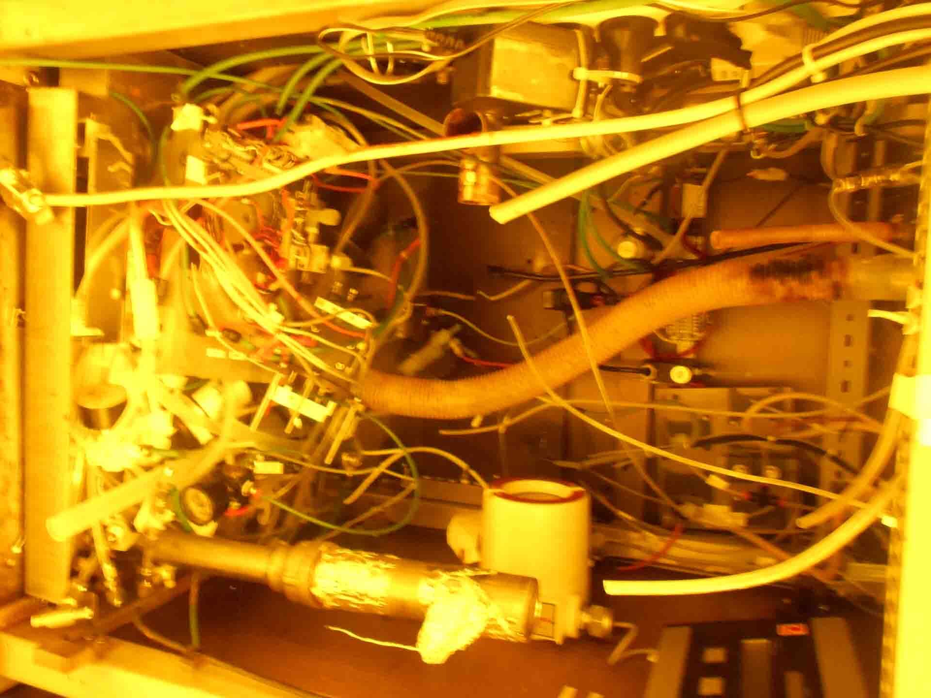
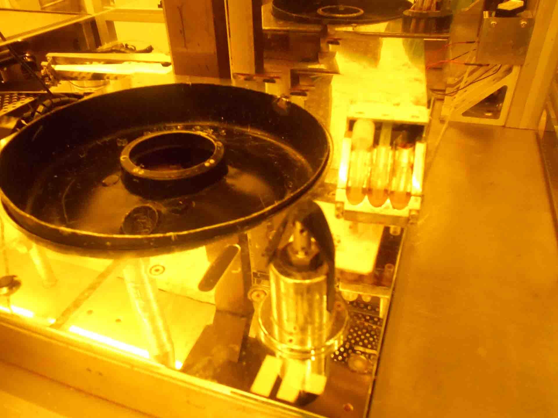
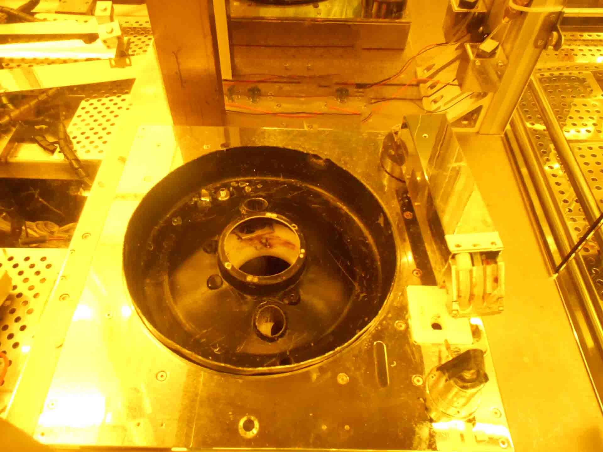
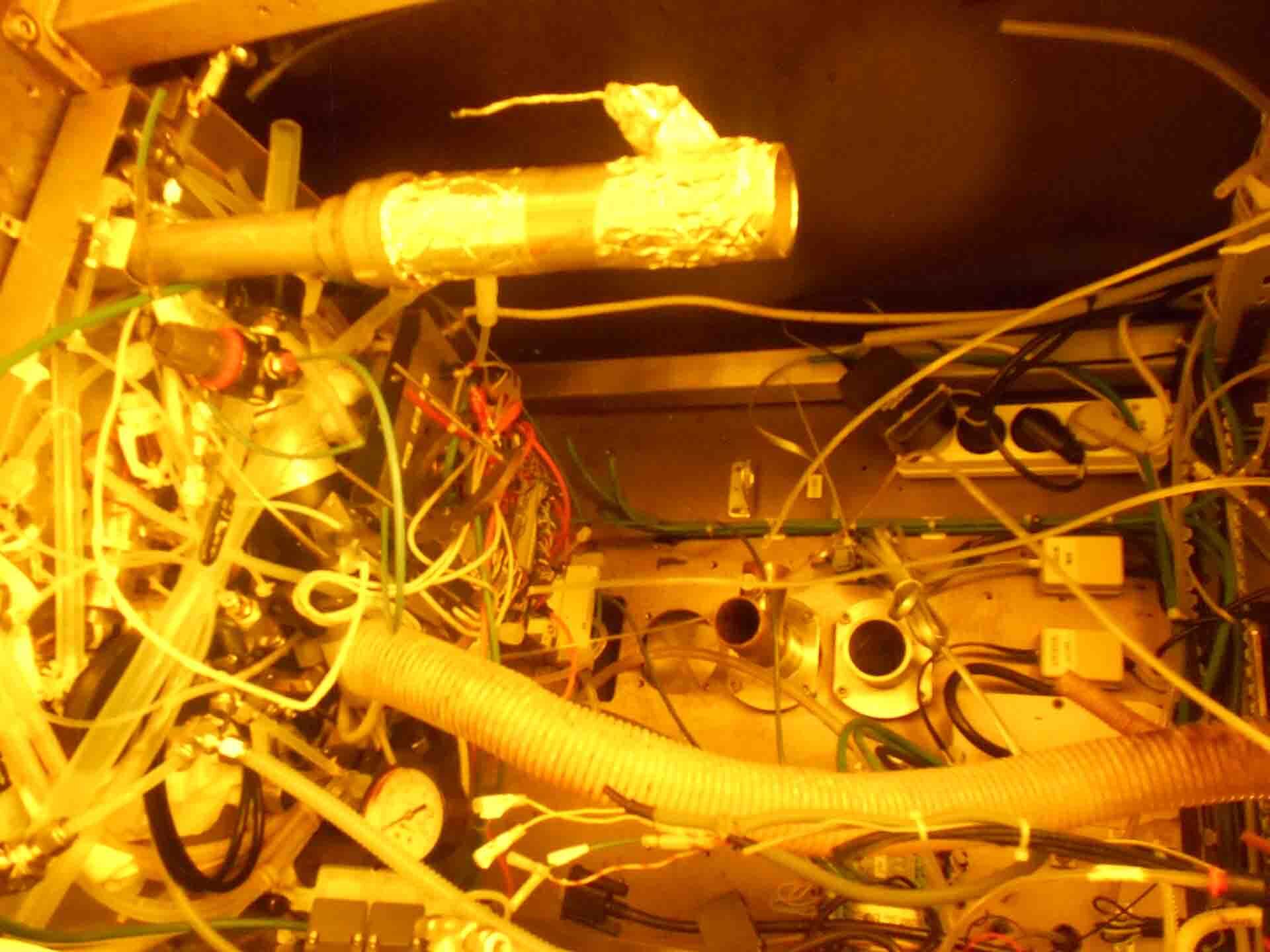
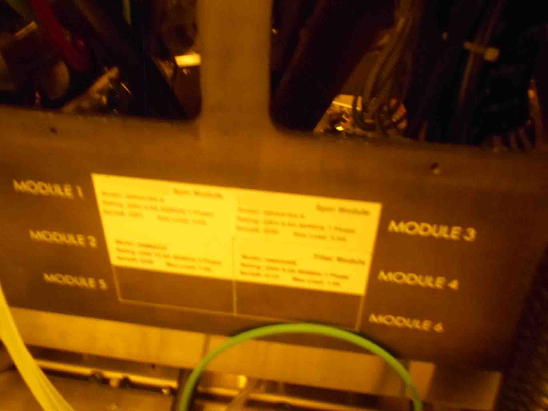
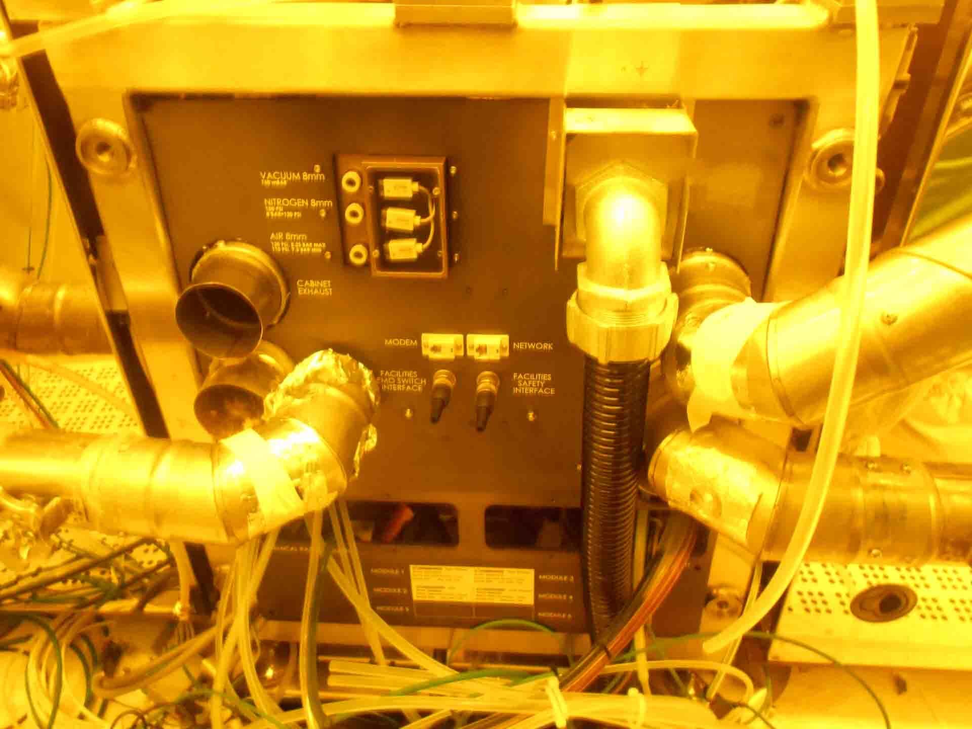
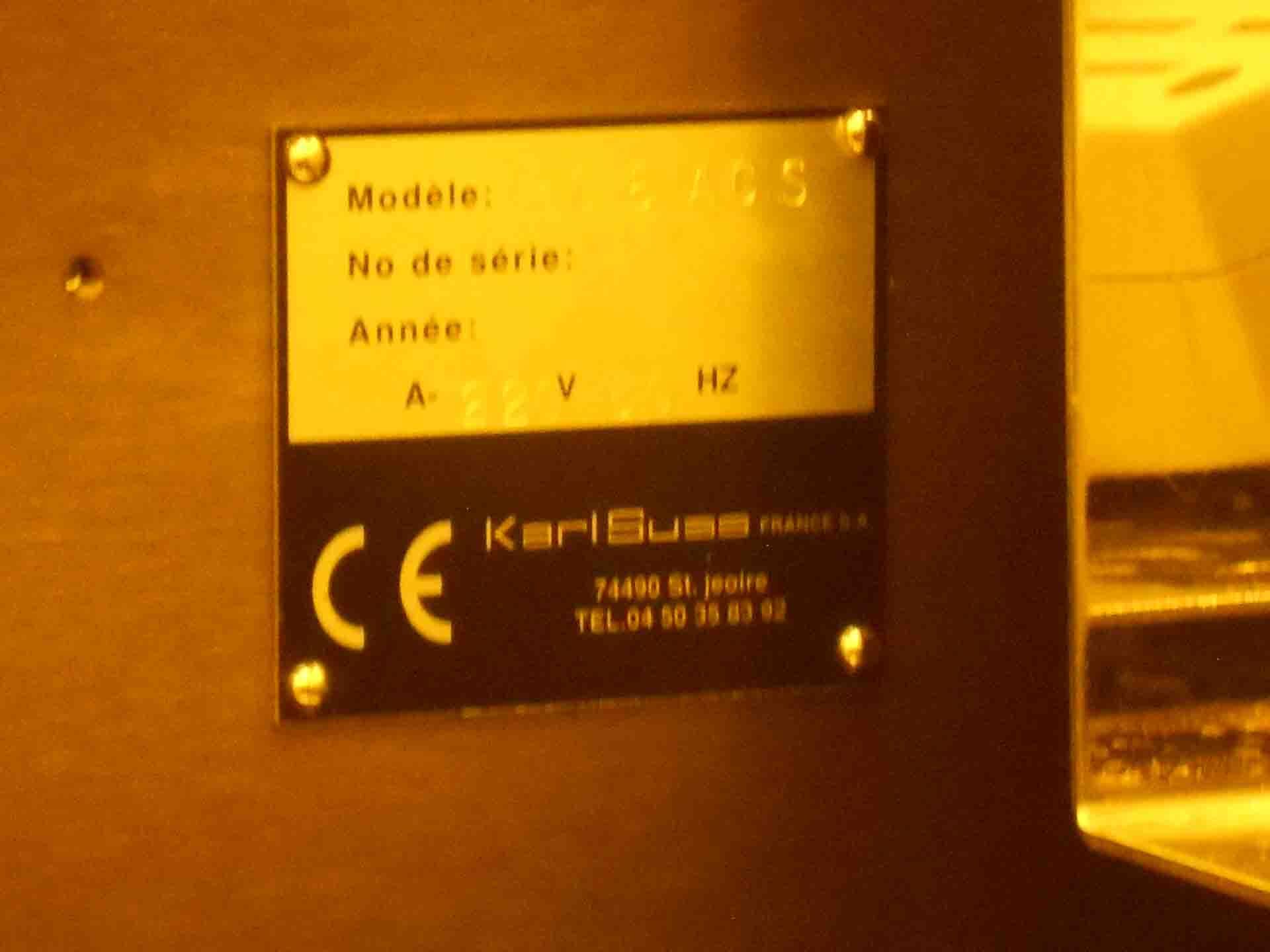
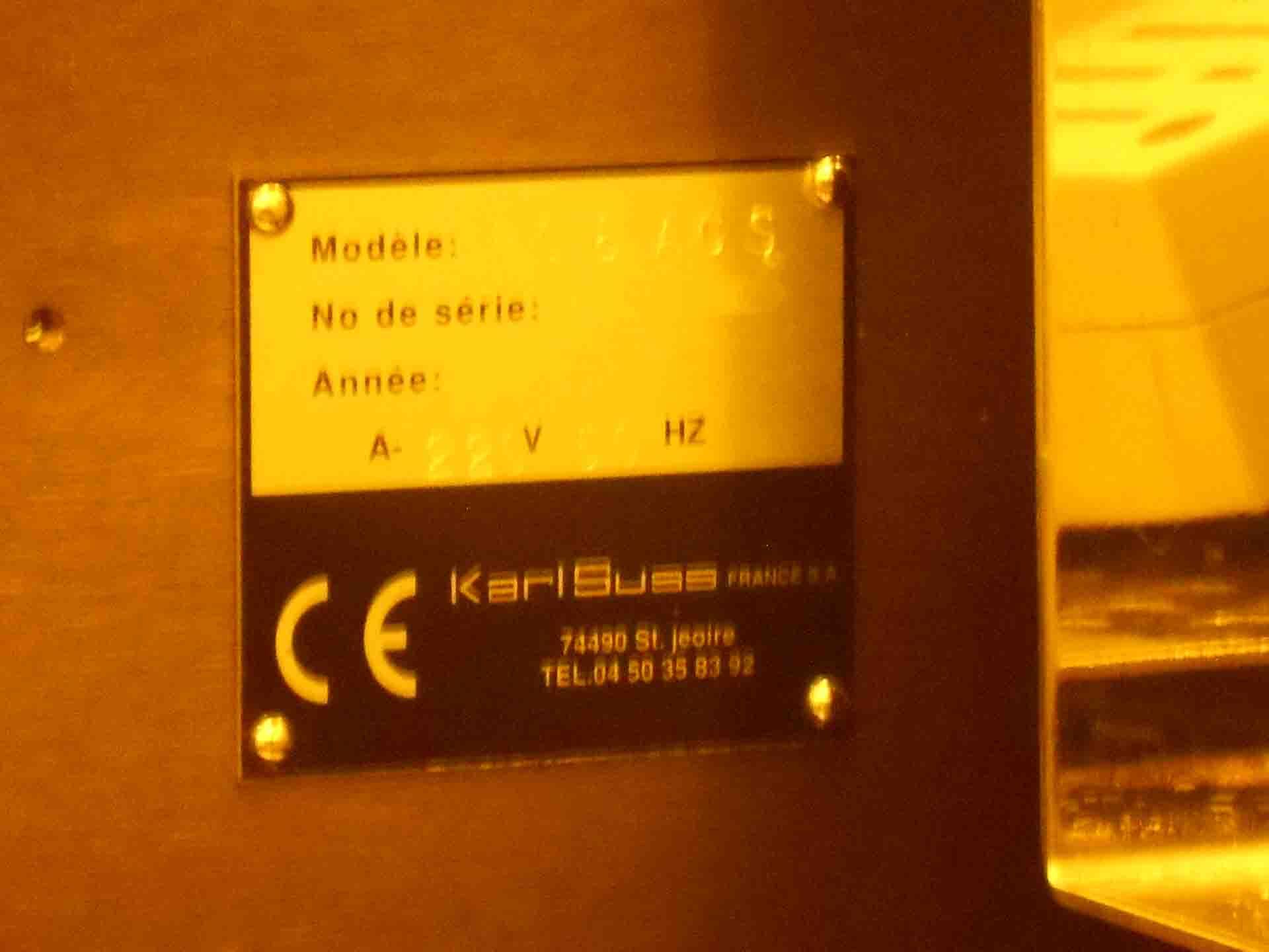
ID: 9353323
Vintage: 2001
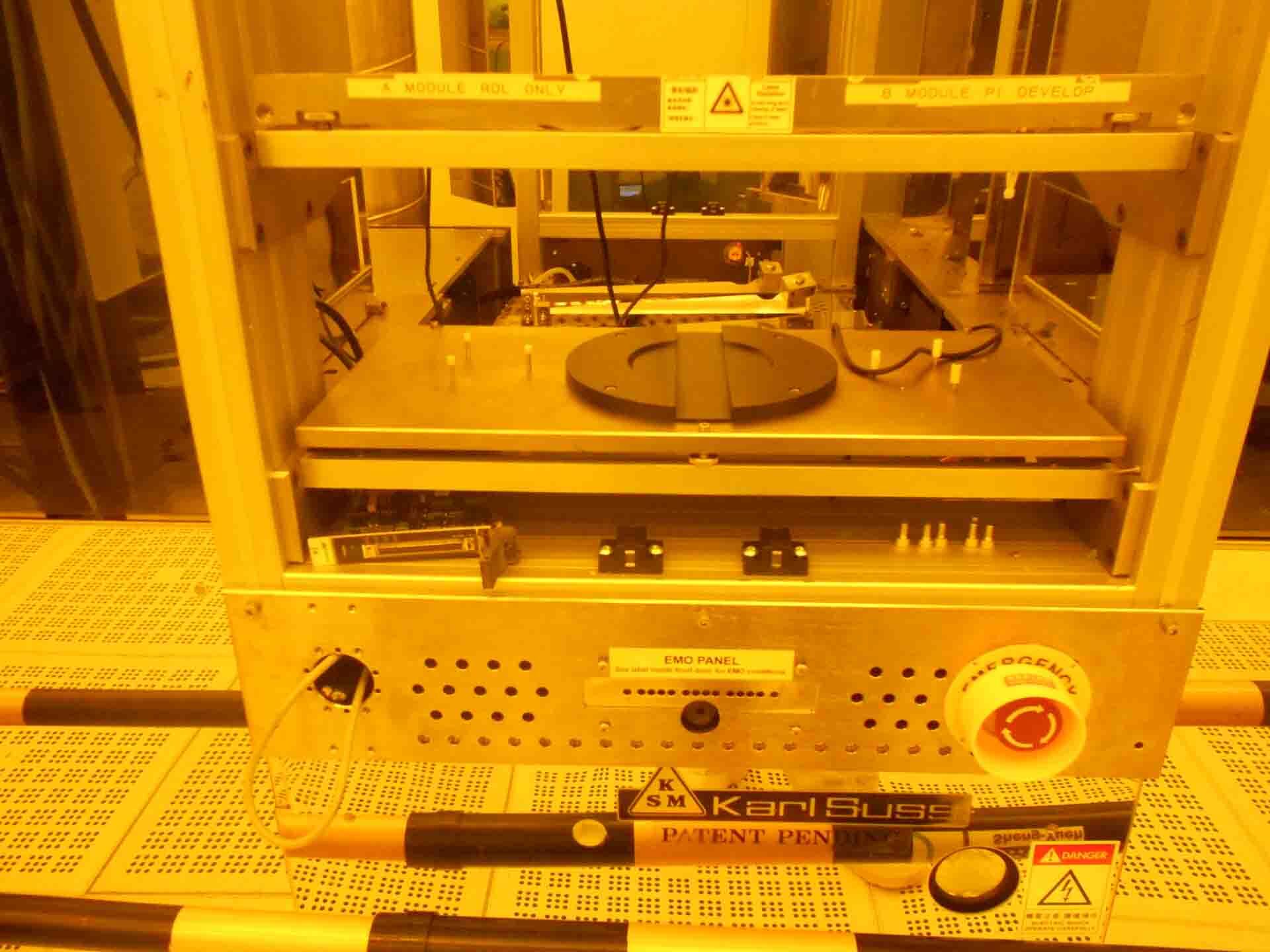
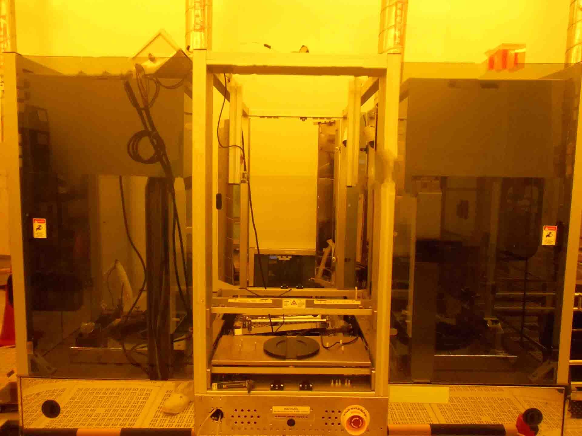
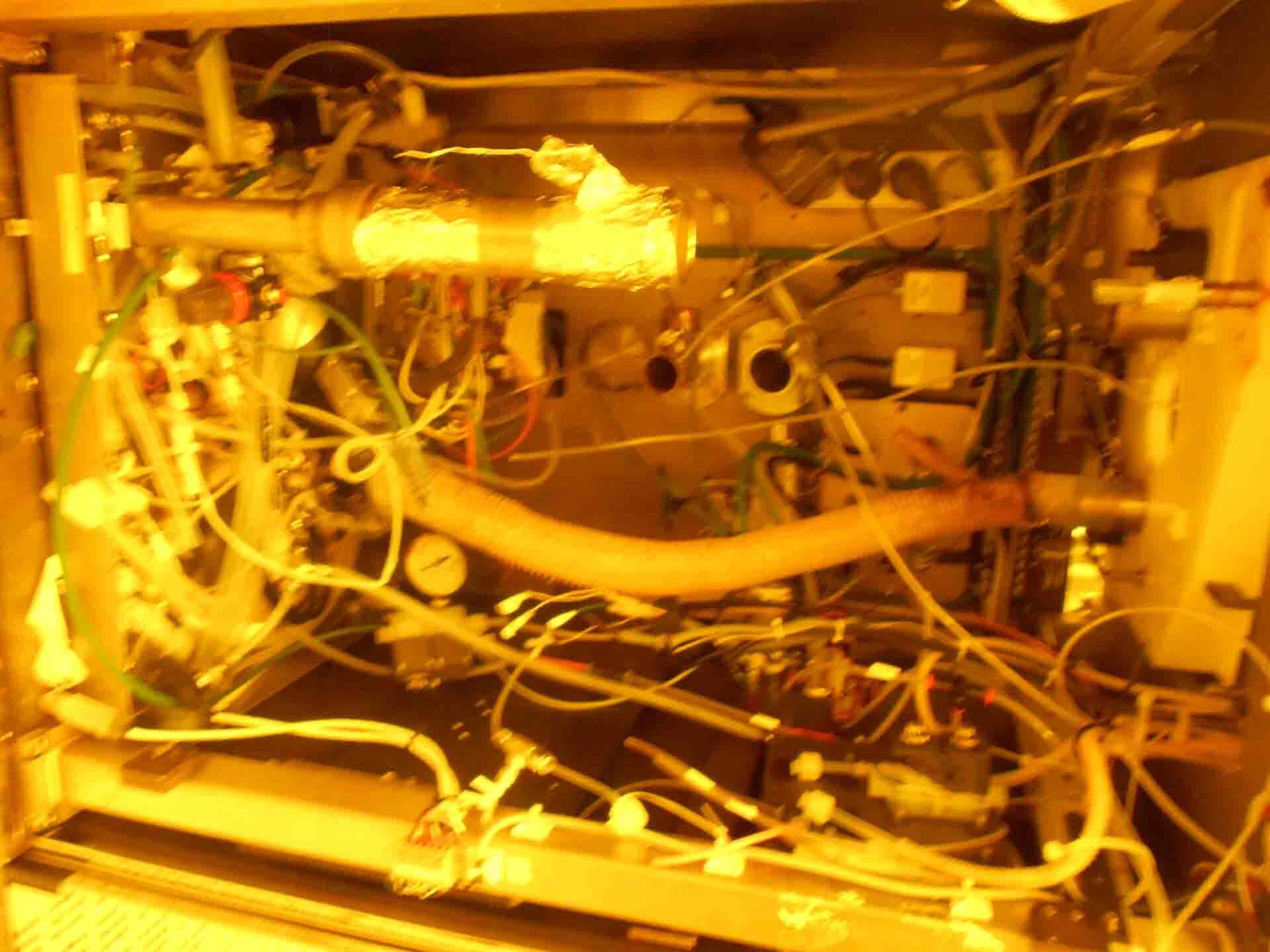
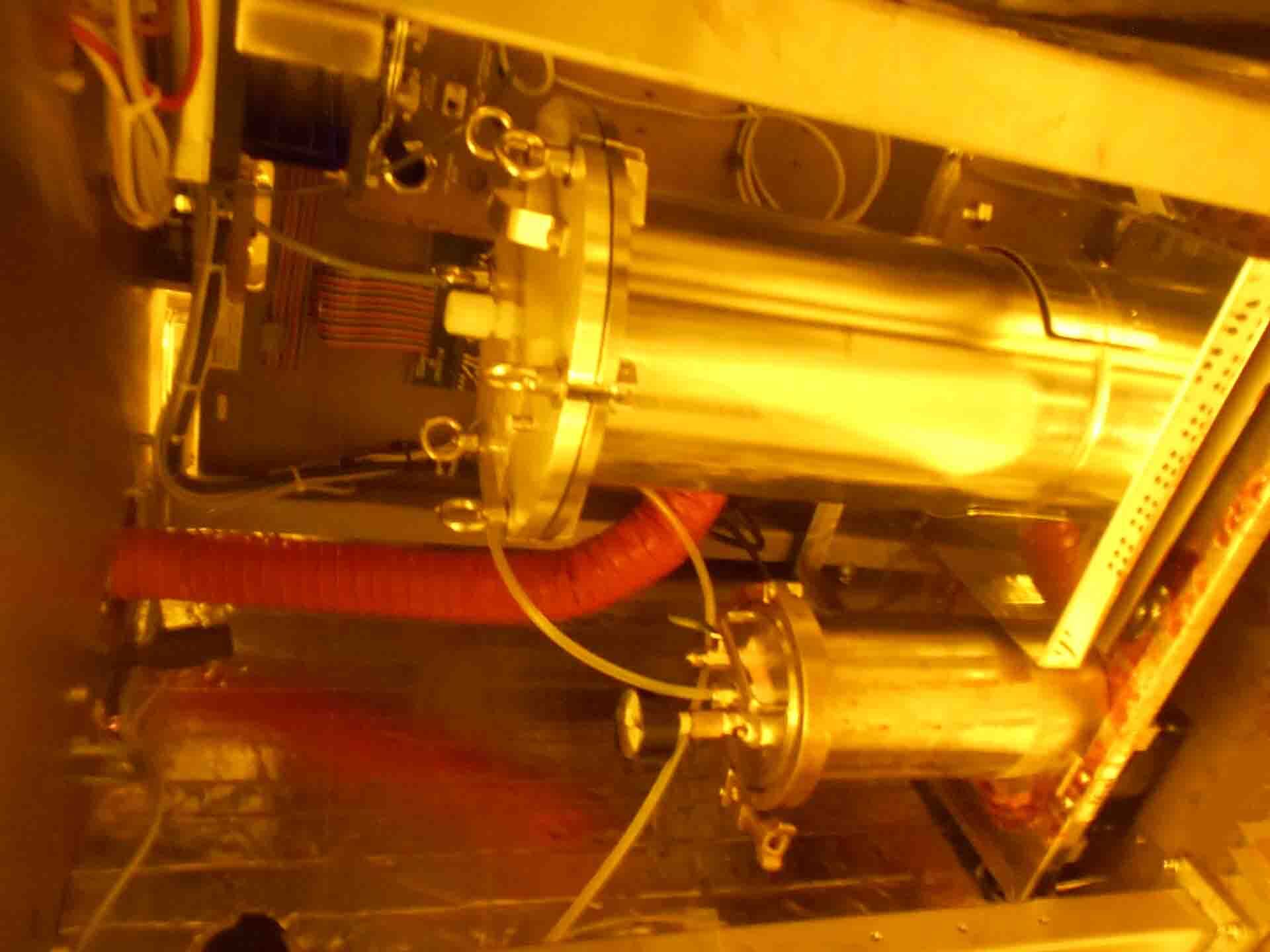
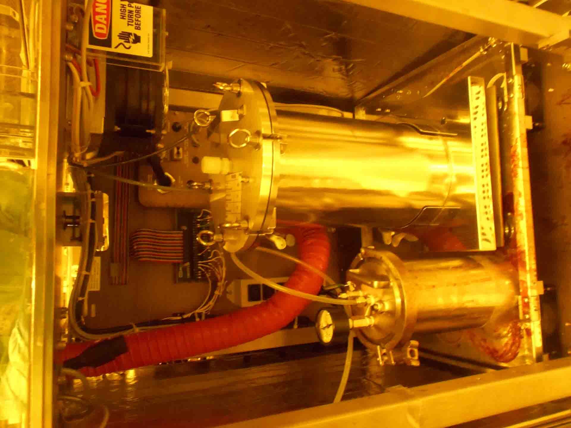
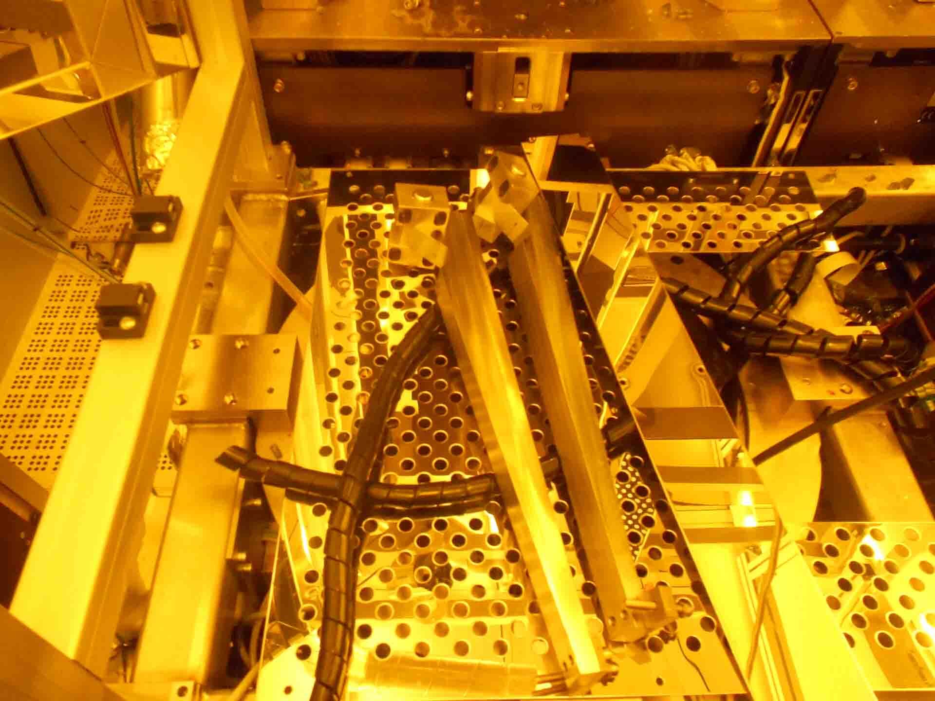
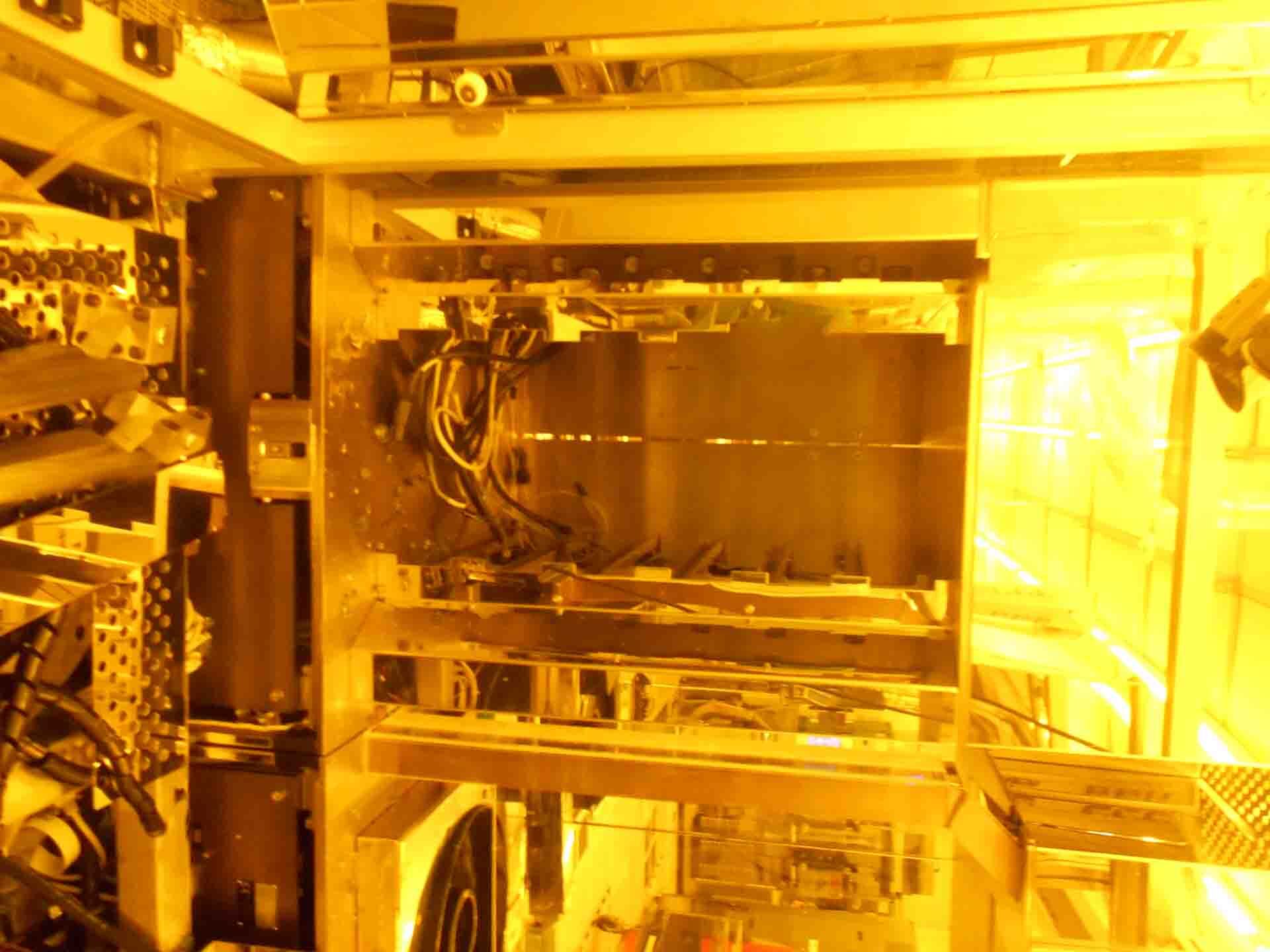
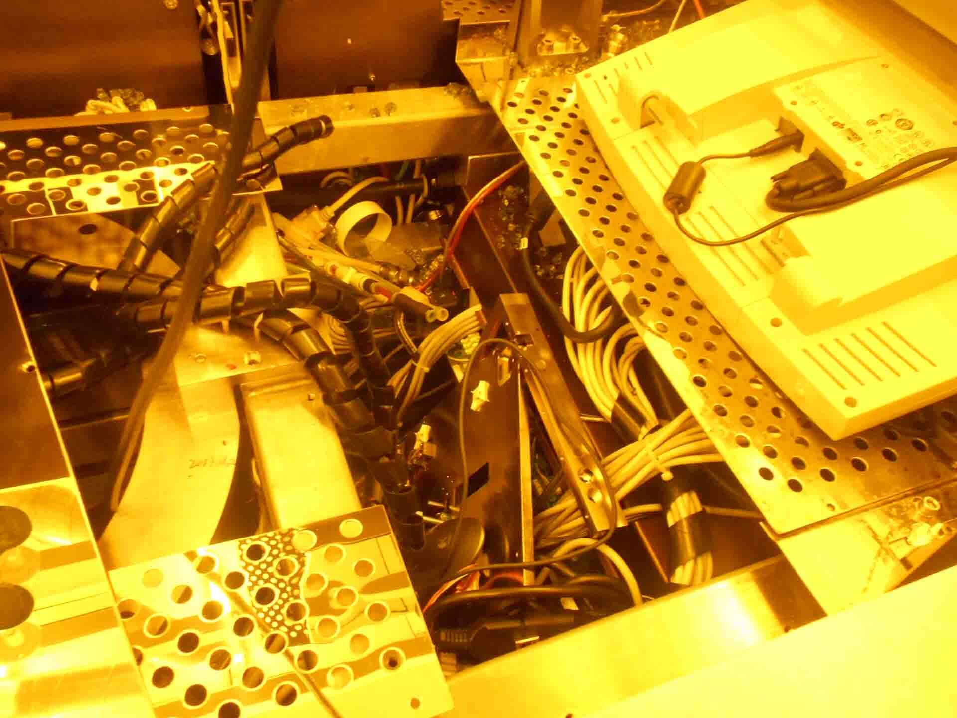
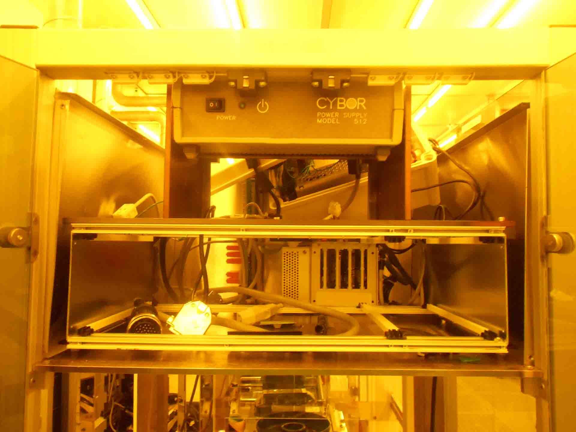
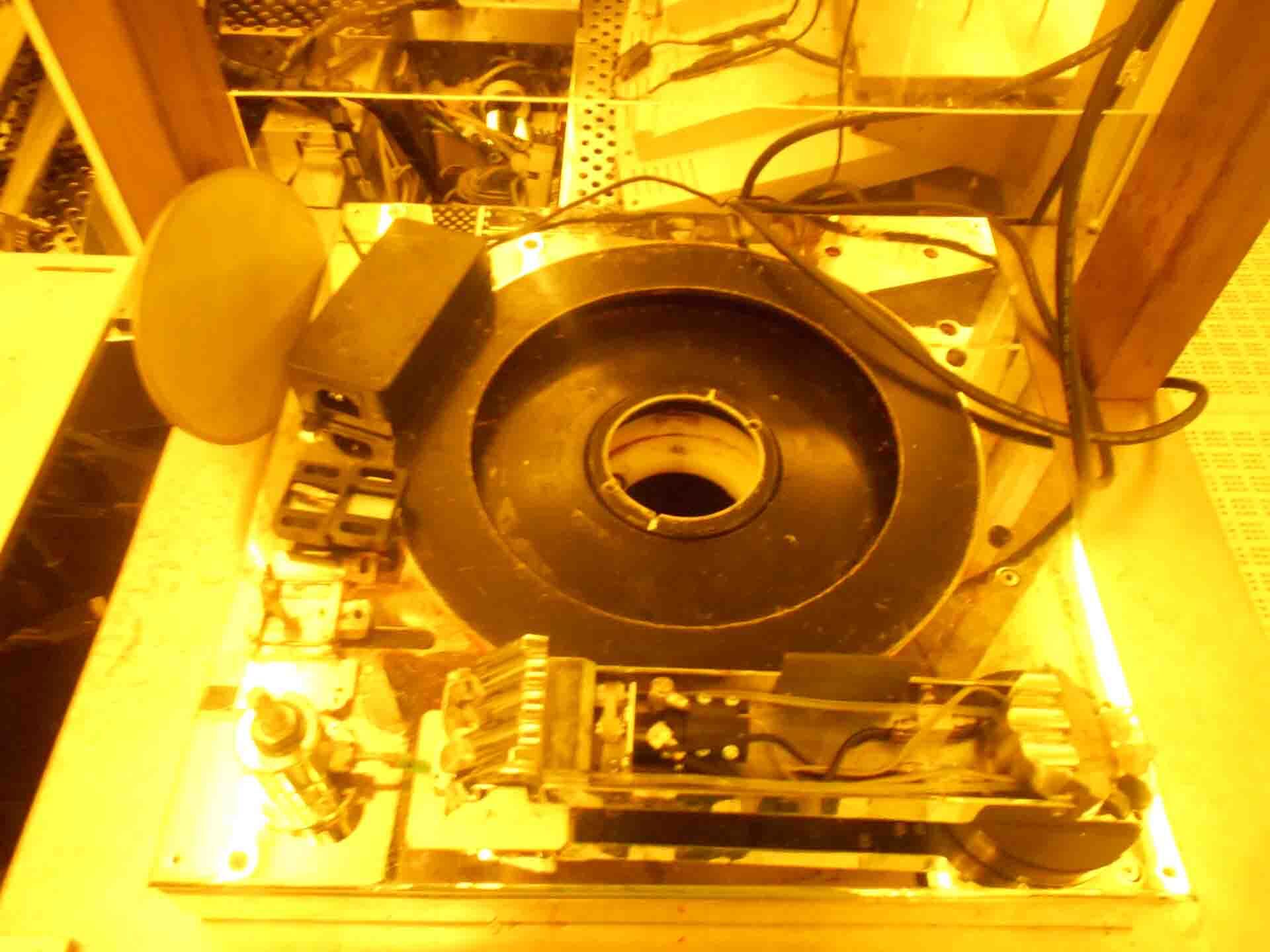
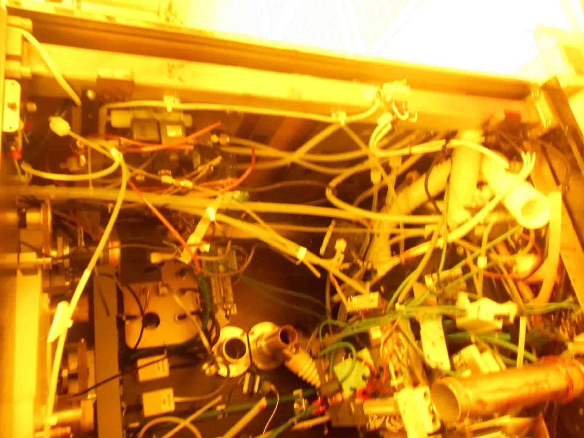
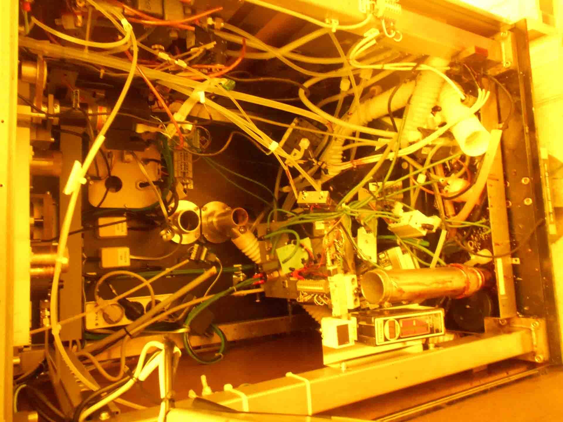
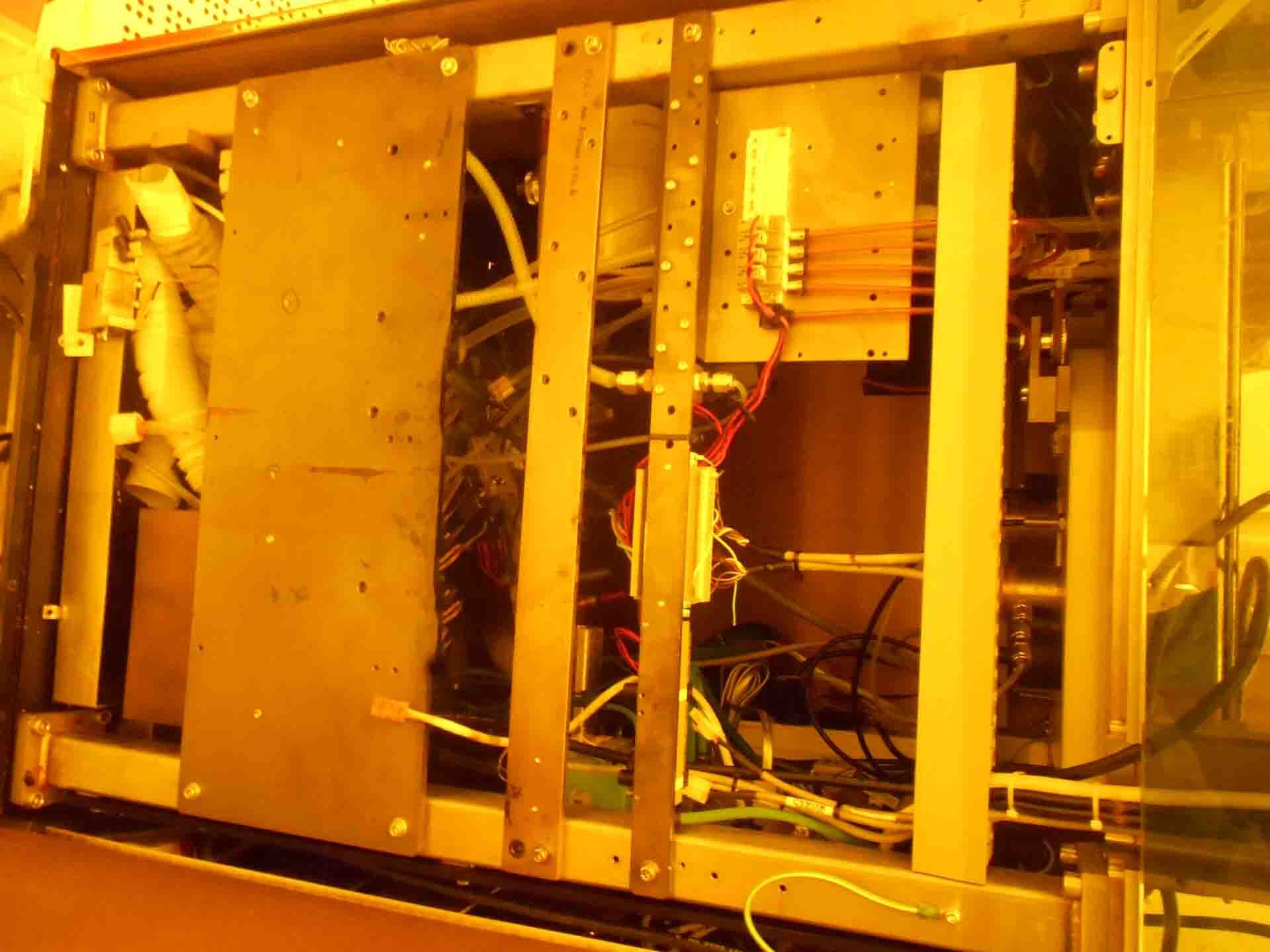
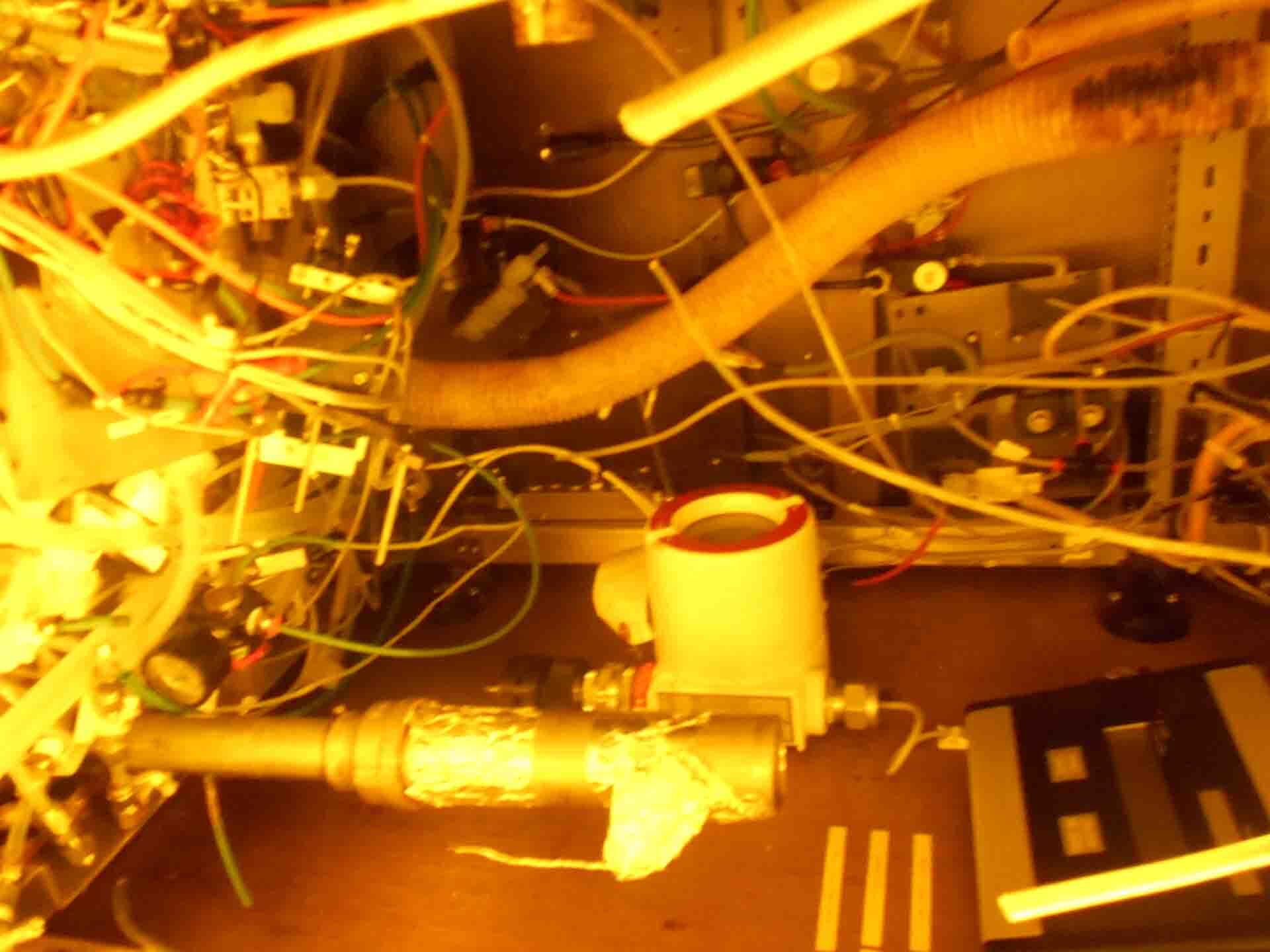
Coater / Developer system, parts machine
Missing parts:
Robot
Loadport
Hot plate
Chuck
PC
2001 vintage.
KARL SUSS / MICROTEC ACS 200 is a photoresist coating and developing equipment designed for use in the fabrication of wafer level devices. The system enables precise etching of intricate features into the surface of a wafer or other microstructure, allowing it to be used in the creation of advanced micro-electronic and opto-electronic devices. The unit is composed of three major parts, an exposure station, a coating station and a spin-rinse station. The machine is designed for direct coat, bake and develop operation using a variety of developer solutions. The exposure station uses ultraviolet (UV) light in order to uniformly cure the photoresist onto the wafer surface. The UV light is focused through a reticle onto the wafer, exposing the area which requires etching. The light exposure is programmed and controlled via a personal computer and the exposure can be set to any desired level. The coating station is used to apply the photoresist material onto the wafer surface. The photoresist material is contained within a cartridge, which is installed into the machine when required. The photoresist is then coated onto the wafer surface in an even film using a spin-coating technique. The spin-rinse station is used to remove any excess photoresist material from the wafer surface. The wafer is placed inside the spin-rinse station where it is submerged into a chemical solution, such as a MICROTEC D 810 developer or a KARL SUSS D 820 developer. This solution will then mix with the photoresist material on the surface of the wafer, causing it to dissolve any excess material. Once the rinse process is complete, the wafer can be removed and allowed to air dry. MICROTEC ACS200 is a versatile and reliable tool, capable of producing complex micronoscopic features quickly and accurately. It is designed to provide reliable and consistent performance, with a full range of features enabling the user to achieve maximum yields from their devices. The asset is widely employed in the production of micro-electronic and opto-electronic devices, and is a valuable tool in the development and manufacture of cutting edge technology.
There are no reviews yet