Used KARL SUSS / MICROTEC Gamma #293745275 for sale
URL successfully copied!
Tap to zoom
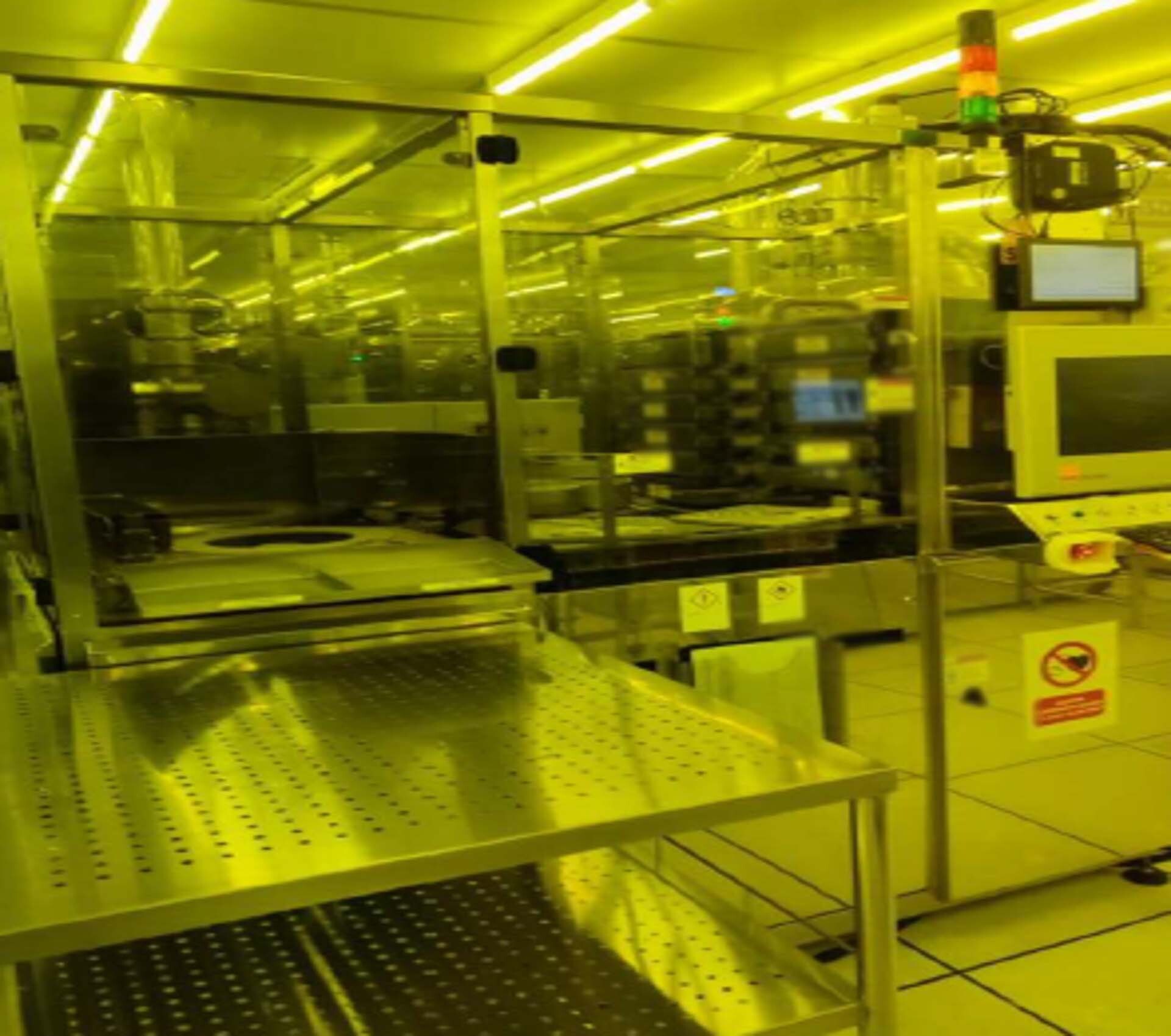

KARL SUSS / MICROTEC Gamma is a photoresist equipment which is used to develop fine patterns onto various surfaces. The photoresist system is composed of three major components: the wafer stage, the mask holder and the illumination unit. The wafer stage is what holds the surface to be patterned. It consists of a highly precise stepping motor which is used to accurately move the surface in the X, Y and Z directions. The mask holder is mounted onto the wafer stage and holds the photomask. The photomask is used to transfer the pattern from the mask onto the surface. The illumination machine consists of a powerful UV source, typically a mercury arc lamp, which is used to shine light through the mask in order to expose the photoresist. MICROTEC Gamma is a highly accurate tool and is capable of consistently producing high-resolution fine patterns. It operates in a standing-wafer mode which maintains a constant surface distance and exposure distance between the exposure source and the exposed surface. The wafer stage has a positional resolution of one micron and repeatability of +/- 0.005 microns allowing for higher accuracy pattern positioning. Additionally, the mask holder is capable of angles from 0 - 20 degrees in steps of 0.1 degrees eliminating any distortion in patterns due to angular differences. KARL SUSS Gamma can be used in conjunction with a wide variety of photoresists including positive and negative photoresists as well as thick resists. This photoresist asset utilizes a two-stage exposure approach which means that the pattern exposed is accurate to finer details and extremely uniform in area with no pin-holing or shadowing. Additionally, due to its precise X,Y,Z positioning model, this equipment can be used for patterning multiple layers at various technologies and various features sizes, such as resist lines as thin as 50nm. Gamma is the ideal photoresist system for developing submicron size, single and multi-layer patterns onto a variety of substrates. Its robust design, high accuracy and repeatability make it ideal for research, development, and production of intricate patterns in the nano-electronics domain.
There are no reviews yet