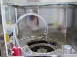
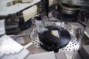
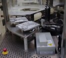
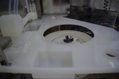
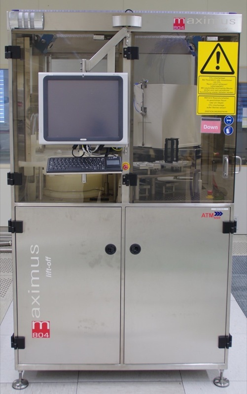
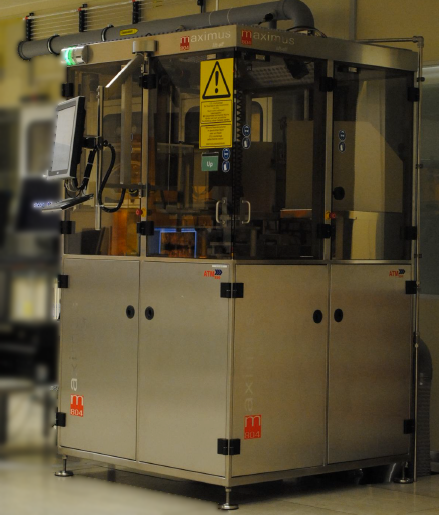
Used MAXIMUS 804 #9013168 for sale
URL successfully copied!
Tap to zoom


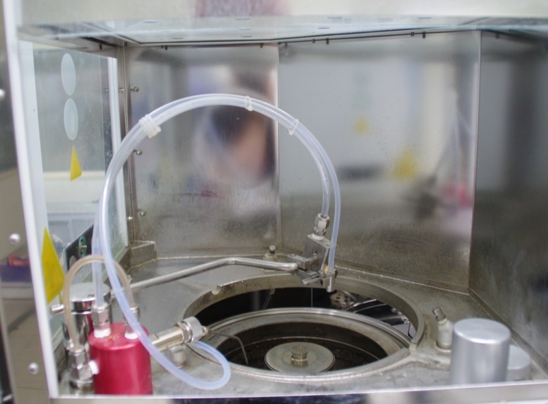

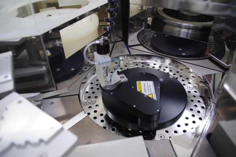

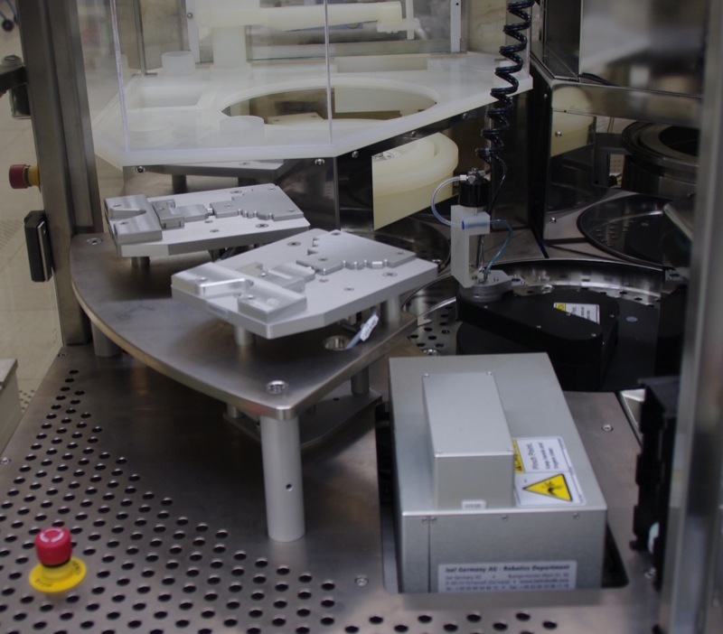

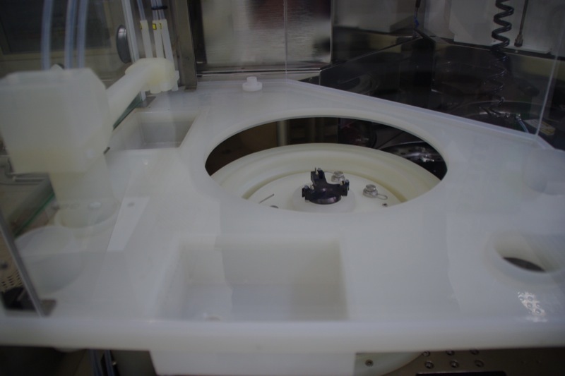




ID: 9013168
Vintage: 2010
Resist stripper
Automatic lift-off and cleaning system for 2”, 3”, 4”, and 6" wafer
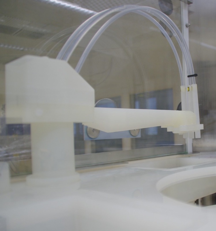
3-axis robot
Class 1
Flat touch screen monitor
Motor spinning speed 1 – 1000 rpm
Motor acceleration 1-50000 rpm/sec
5 liter waste tank with high-level sensor
Stainless steel tank for hot nmp
Carrier agitation and lifting unit
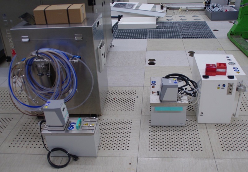
Media recirculation unit
Cryostat for heating and cooling
Up to 80°c
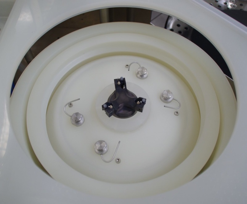
Lift- off process chamber
Brushless dc motor
Drain filter for lift off processing
High pressure system nmp pressures from approx 10 bar up to 180 bar
Programmable chamber rinse system with nmp
Cleaner module (di- water and ipa rinse)
Fully automatic and programmable cassette-to-cassette cleaning system
CE Marked
De-installed
2010 vintage.
MAXIMUS 804 is a photoresist equipment designed for semiconductor wafer fabrication. It utilises advanced, precision technology to ensure quality control in sample processing and analysis. The system requires a variety of advanced processes to ensure reliable sample analysis. This includes lithography, etching, photoresist application, chemical mechanical planarization (CMP), and deposition. The photoresist unit significantly reduces the cost of semiconductor wafer fabrication and is capable of producing results with higher accuracy. This is achieved by using a vacuum chuck to effectively hold the wafer and ensure accurate contact between the wafer and each of the different components within the machine. This is followed by the precise application of photoresists. The photo resists are used to protect the wafer from etching and chemical processes, which are integral to semiconductor fabrication. The photoresist can be optically exposed through an advanced spectrophotometer and reflective optical tool which ensures repeatable patterns in sample analysis and fabrication. The asset is capable of delivering highly precise results, as it utilises nanometer-scale films and resists to selectively etch structures on the wafer. In addition, it uses CMP to ensure uniformity and planarity of the sample. During lithography, the photoresist is selectively applied over the wafer in the predetermined pattern. The wafer is then exposed to an ultraviolet (UV) light to selectively pattern the photoresist. Finally, the patterned photoresist can be etched and removed, leaving behind the wafer with precise patterns formed according to the design. 804 photoresist model also includes advanced testing and analysis features. This includes advanced analysis techniques such as laser interferometry, optical scattering, and edge resolution. These features ensure that the wafers meet the exacting standards required for semiconductor fabrication. Overall, MAXIMUS 804 photoresist equipment utilises advanced technology and precision process techniques to provide reliable and cost effective semiconductor wafer fabrication. The system can be used to form precise patterns with repeatable accuracy, and can be used to make products with reliable performance and long lasting reliability.
There are no reviews yet


