Used MIKASA MS-B150 #293797162 for sale
URL successfully copied!
Tap to zoom
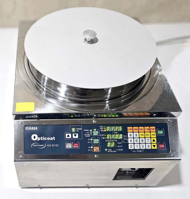

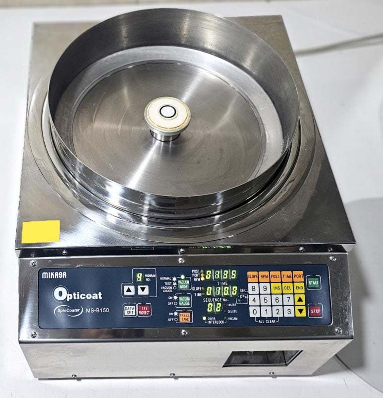
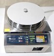
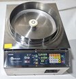
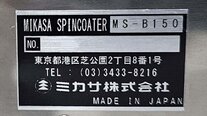
MIKASA MS-B150 photoresist equipment is a cutting-edge equipment used in semiconductor manufacturing processes, particularly in photolithography. This system is designed to apply photoresist materials onto semiconductor wafers with precision and consistency, essential for creating intricate patterns and features on the wafer surface. MS-B150 offers advanced capabilities that enable semiconductor manufacturers to achieve high-resolution patterning and superior yields in their production processes. At the core of MIKASA MS-B150 unit is its advanced dispensing mechanism, which ensures precise and uniform deposition of photoresist material onto the wafer surface. This mechanism is equipped with high-precision pumps and nozzles that enable controlled dispensing of photoresist in ultra-thin layers, crucial for achieving submicron resolution in semiconductor patterning. The machine's dispensing process is fully programmable, allowing users to adjust parameters such as flow rate, dispensing speed, and coating thickness to meet specific process requirements. In addition to its dispensing capabilities, MS-B150 tool offers features for post-application processes such as spinning, baking, and developing. After the photoresist material is dispensed onto the wafer, the asset can spin the wafer at high speeds to achieve a uniform coating thickness. Following the spinning process, the wafer can be baked in the model's integrated hotplate to remove solvents and achieve optimal adhesion of the photoresist to the wafer surface. MIKASA MS-B150 also supports development processes to selectively remove exposed or unexposed photoresist areas, essential for defining the desired pattern on the wafer. One of the key advantages of MS-B150 equipment is its versatility in handling various types of photoresist materials, including positive and negative photoresists. Positive photoresists are typically used to create features on the wafer surface by selectively removing exposed areas, while negative photoresists enable patterning by selectively retaining exposed areas. The system's compatibility with different photoresist formulations allows semiconductor manufacturers to adapt to diverse process requirements and achieve optimal results in their fabrication processes. Moreover, MIKASA MS-B150 unit is designed for high-throughput manufacturing environments, offering fast cycle times and efficient wafer handling capabilities. The machine's automated controls and advanced software enable seamless integration with other semiconductor manufacturing equipment, providing a streamlined workflow for production processes. With its robust construction and reliable performance, MS-B150 tool is built to meet the demanding requirements of semiconductor fabrication facilities and ensure consistent and repeatable results in photoresist application processes. Overall, MIKASA MS-B150 photoresist asset represents a state-of-the-art solution for semiconductor manufacturers seeking to achieve precise patterning and high-resolution features on semiconductor wafers. With its advanced dispensing capabilities, post-application processing features, and compatibility with various photoresist materials, MS-B150 model offers semiconductor manufacturers a versatile and reliable tool for enhancing their manufacturing processes and achieving superior yields in semiconductor production.
There are no reviews yet