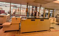
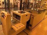
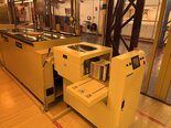
Used MUSCAT T200 #293738316 for sale
URL successfully copied!
Tap to zoom
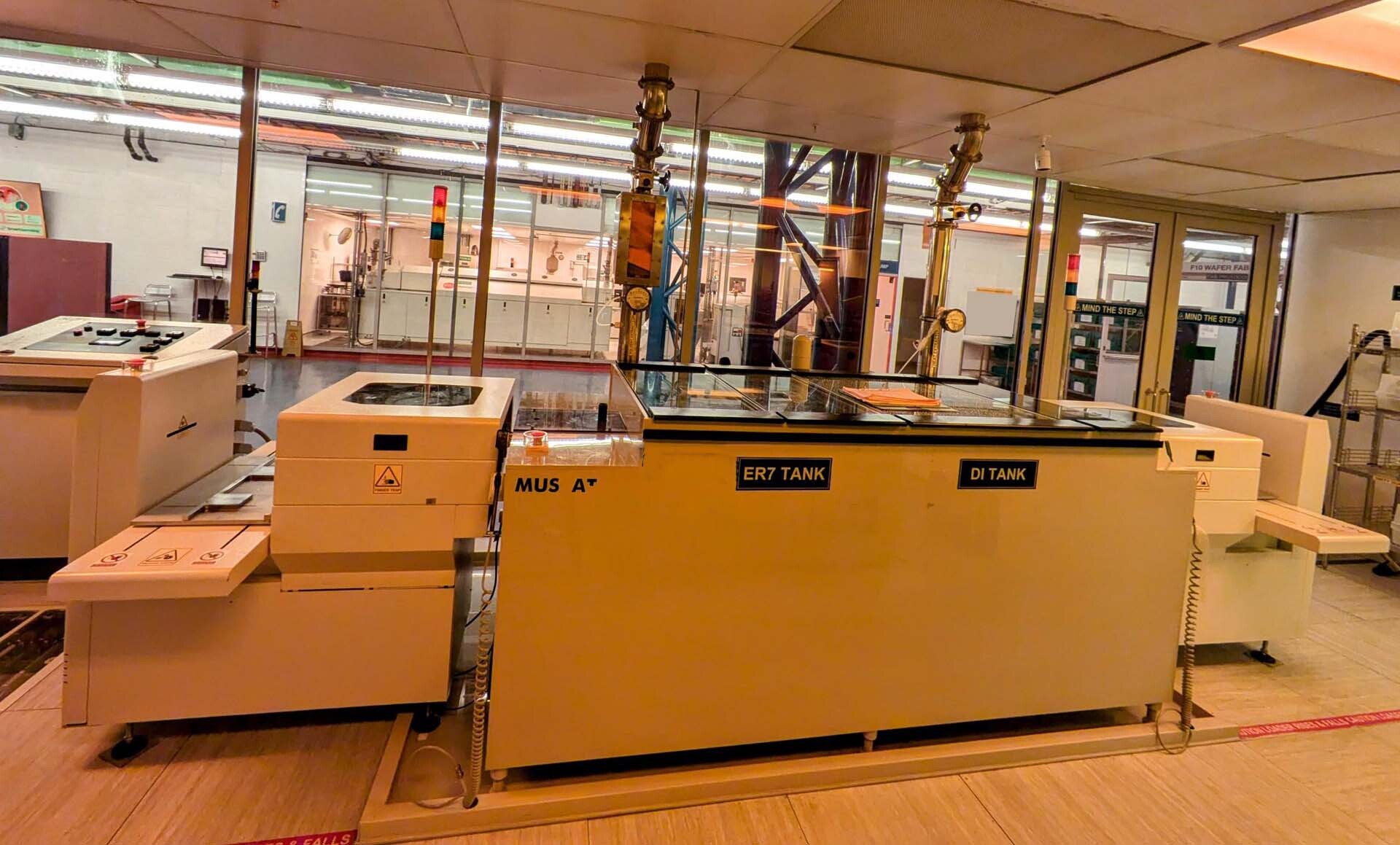
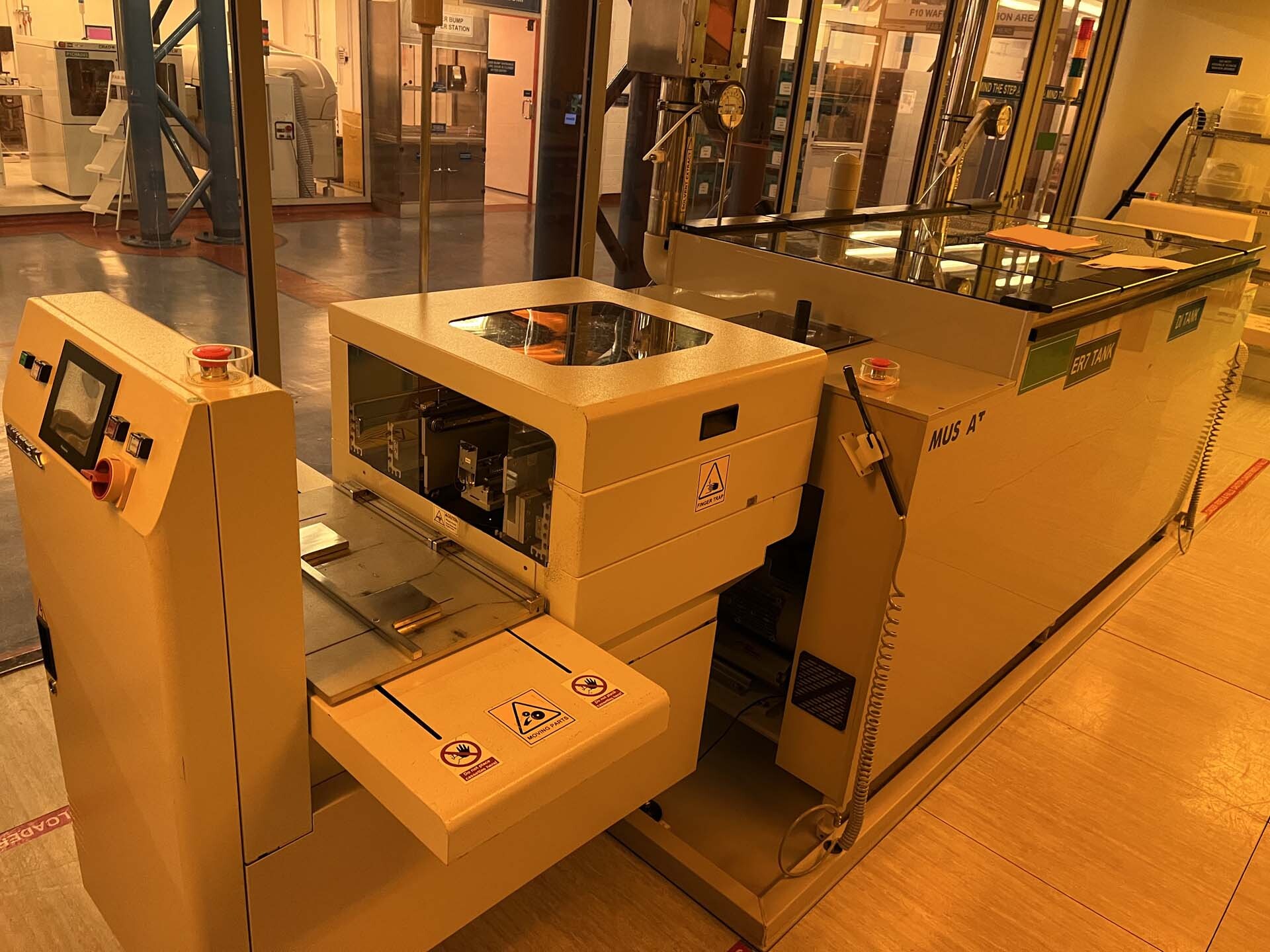
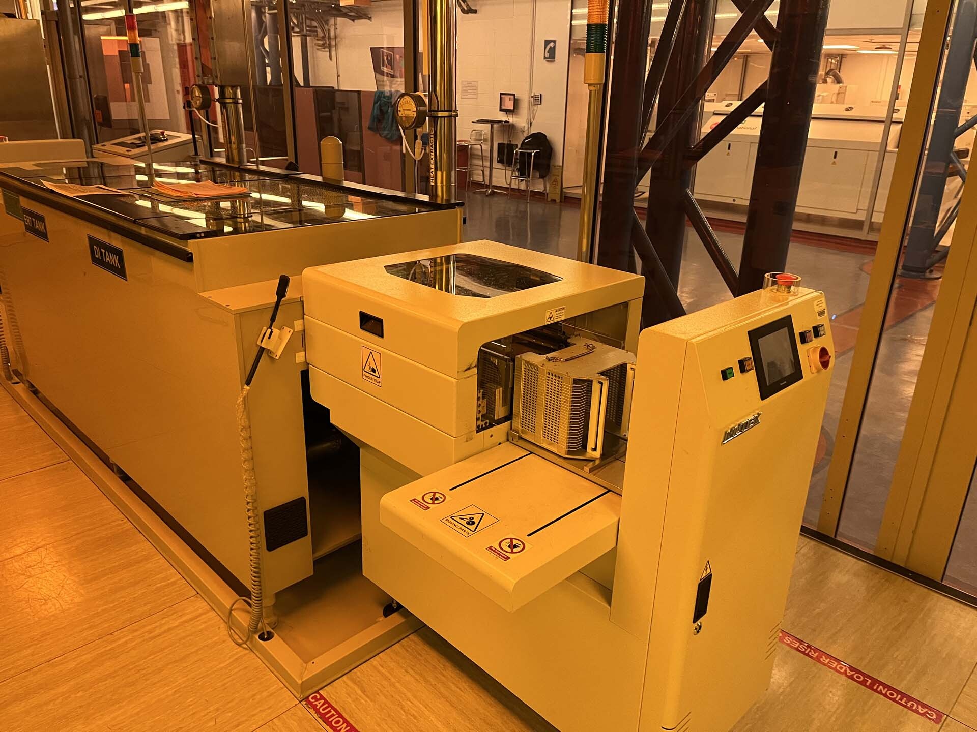
MUSCAT T200 is a specialized photoresist equipment designed for advanced photolithography processes used in semiconductor manufacturing and other microfabrication applications. A photoresist is a light-sensitive material that undergoes chemical changes when exposed to UV light, serving as a mask for transferring patterns onto substrates. T200 photoresist system offers high-performance characteristics that enable precise control over pattern resolution, line edge roughness, and process compatibility for demanding semiconductor fabrication needs. Key Features of MUSCAT T200: 1. Advanced Chemistries: T200 photoresist unit utilizes advanced chemistry formulations that are optimized for high-resolution patterning and excellent adhesion properties. These chemistries allow for the formation of well-defined patterns with sharp edge acuity and minimal defects, critical for achieving high yields in semiconductor manufacturing. 2. High Sensitivity: MUSCAT T200 photoresist machine exhibits high sensitivity to UV light exposure, enabling rapid patterning processes with reduced exposure times. This high sensitivity is essential for increasing throughput in semiconductor fabrication facilities and achieving tight control over feature sizes and dimensions. 3. Thermal Stability: T200 offers exceptional thermal stability, allowing for the utilization of multiple processing steps such as post-exposure bake, development, and etching without compromising pattern fidelity. The tool's thermal stability ensures consistent performance across a wide range of process conditions, contributing to the reproducibility of pattern transfer processes. 4. Compatibility with Multiple Substrates: MUSCAT T200 photoresist asset is compatible with various substrate materials commonly used in semiconductor manufacturing, including silicon, silicon dioxide, and III-V compound semiconductors. This compatibility ensures flexibility in process integration and enables the fabrication of complex device structures with diverse material compositions. 5. Process Control and Uniformity: T200 facilitates precise process control and uniformity in pattern transfer processes, resulting in high-quality pattern replication with minimal variation. The model's excellent uniformity across large substrate areas ensures consistent device performance and enhances the overall yield in semiconductor production. 6. Low Cost of Ownership: MUSCAT T200 is designed to offer a low cost of ownership by optimizing material consumption, reducing process steps, and minimizing waste generation. The equipment's efficiency in material utilization and process workflow contributes to overall cost savings for semiconductor manufacturers, making it a cost-effective solution for high-volume production. Applications of T200: MUSCAT T200 photoresist system is widely used in advanced semiconductor manufacturing processes such as optical lithography, electron beam lithography, and nanoimprint lithography. It is employed in the fabrication of integrated circuits, MEMS devices, photonic components, and other microscale devices requiring precise patterning and high-resolution features. In conclusion, T200 represents a state-of-the-art photoresist unit that offers superior performance, reliability, and versatility for a wide range of semiconductor fabrication applications. With its advanced chemistries, high sensitivity, thermal stability, substrate compatibility, process control, and cost-effectiveness, MUSCAT T200 is a valuable tool for achieving advanced patterning requirements in the semiconductor industry.
There are no reviews yet