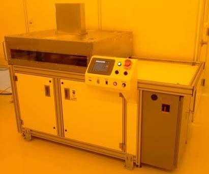
Used OWENS DESIGN Gen 2 #9234063 for sale
URL successfully copied!
Tap to zoom


ID: 9234063
Vintage: 2013
Spin coater
Water soluble polymer coating
For LCD glass substrates, 24"
2013 vintage.
OWENS DESIGN Gen 2 is a digital photoresist equipment that was specifically designed to transform traditional masking processes in the semiconductor manufacturing market. This system is one of the most advanced photoresist processes available, based on a multi-layer lithography technology that enables wafer-level control of photomasking. It is ideal for creating precise patterns with resolutions below 10 nanometers on very small or complex circuit features. The photoresist unit relies on the optical effect of photomodification of a composite photosensitive material on a specific surface. This photosensitive material is a coat of chemicals, which includes a light-sensitive agent and a developer. When exposed to light from a specific wavelength, the light-sensitive agent changes while the developer remains unchanged. A precise mask with a laser-cut pattern is placed over a wafer and an exposure of a specific wavelength is used to expose the photosensitive material. After exposure, the wafer is treated with a developer chemical which changes the exposed photosensitive material, creating a precise pattern. Gen 2 photoresist machine is highly reliable and predictable and works with a variety of lithography processes. It offers a variety of customizable features including full mask libraries, easy operator programming, multi-positional mask table, wafer tray indexable automatic stages, programmable exposure time controls, and an accessible library of mask recipes. OWENS DESIGN Gen 2 also features an automatic laser-dicing facility that can be used to separate multiple wafers into smaller pieces for further processing. Additionally, as part of its state-of-the-art diagnostic features, the tool has an automated alignment asset and an adaptive focus control feature to ensure accuracy and repeatable process results. In conclusion, Gen 2 photoresist model is a powerful tool for reliable, accurate, wafer-level lithography applications. It provides accurate patterning for improved yield and production time, and significantly reduces cost per wafer through its programmable features.
There are no reviews yet