Used SATISLOH DS 160 #293830377 for sale
URL successfully copied!
Tap to zoom
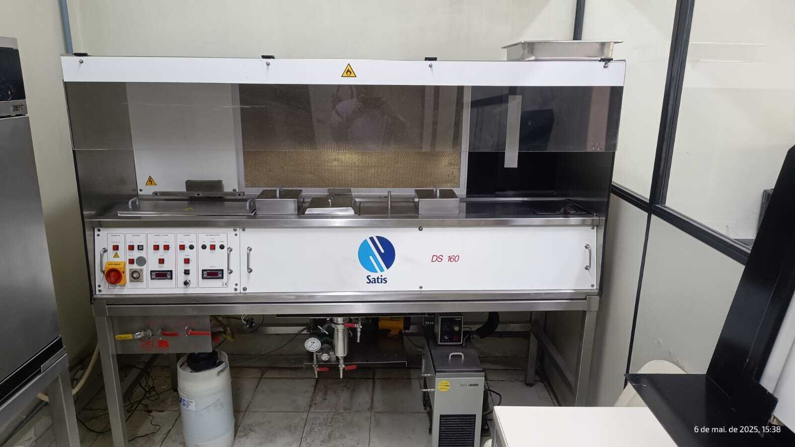

SATISLOH DS 160 is an advanced photoresist equipment used in the semiconductor industry for the precise patterning of integrated circuits and other microelectronic devices. This system consists of a series of components designed to enable high-resolution lithography, crucial for achieving fine line widths and high device densities in semiconductor manufacturing processes. At the core of DS 160 unit is the photoresist material itself, which is a light-sensitive polymer that undergoes chemical and physical changes when exposed to ultraviolet (UV) light. The photoresist contains photosensitive compounds that generate acid or other reactive species upon exposure to light, initiating a series of reactions that ultimately determine the pattern transferred onto the substrate. SATISLOH DS 160 photoresist is formulated to provide excellent resolution, sensitivity, and adhesion properties, allowing for the precise delineation of features on the semiconductor wafer. The lithography process in DS 160 machine begins with the application of the photoresist material onto the substrate, typically a silicon wafer. This can be done using spin coating, in which the wafer is rotated at high speeds to achieve a uniform coating of photoresist. The coated wafer is then soft baked to drive off any solvent and improve adhesion of the photoresist to the substrate. Next, the wafer is exposed to UV light through a mask that contains the desired circuit patterns. The UV light passes through the transparent regions of the mask, exposing corresponding areas of the photoresist on the wafer. The exposure activates the photoactive compounds in the resist, leading to a chemical change in the exposed regions. Following exposure, the wafer undergoes a post-exposure bake (PEB) process to further enhance the reactivity of the photoresist and to stabilize the exposed regions. This step is critical for controlling the shape and dimensions of the pattern transferred onto the substrate. The pattern is then developed by immersing the wafer in a developer solution that selectively dissolves either the exposed or unexposed regions of the photoresist, depending on the type of resist used. This step reveals the patterned features on the substrate, which can then be transferred into the underlying layers through processes such as etching or deposition. SATISLOH DS 160 tool offers several advantages for semiconductor manufacturers. Its high resolution capabilities enable the fabrication of intricate and densely packed circuits, essential for the production of advanced electronic devices. The asset's sensitivity allows for shorter exposure times, leading to increased throughput and efficiency in manufacturing processes. Moreover, DS 160 photoresist model delivers excellent adhesion properties, ensuring good pattern fidelity and uniformity across the wafer. This results in improved device performance and reliability, as well as reduced defects and yield losses during production. In conclusion, SATISLOH DS 160 is a state-of-the-art photoresist equipment that plays a crucial role in the fabrication of semiconductor devices. With its advanced formulations, precise lithography capabilities, and superior performance characteristics, this system enables semiconductor manufacturers to achieve high levels of accuracy and productivity in their manufacturing processes, ultimately contributing to the development of cutting-edge electronic products.
There are no reviews yet