Used SEMITOOL M75 #293740158 for sale
URL successfully copied!
Tap to zoom
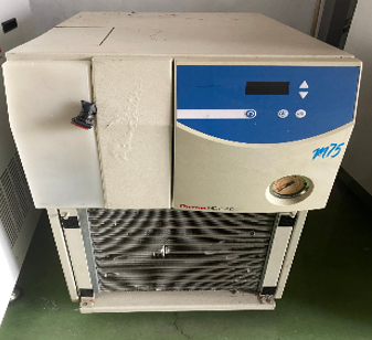

SEMITOOL M75, a cutting-edge photoresist equipment, is a high-performance semiconductor manufacturing tool specifically designed for the precision application and development of photoresist layers in wafer processing. It is an integral component in the fabrication process of integrated circuits and microelectronics, providing the capability to define patterns on semiconductor substrates with extreme accuracy and reliability. One of the key features of M75 system is its advanced technology for coating, baking, and developing photoresist layers on wafers. The unit offers a wide range of functionality and flexibility, allowing for customization based on specific process requirements. It is equipped with state-of-the-art dispensing mechanisms, precision temperature control systems, and intuitive software interfaces to ensure optimal performance and consistent results. SEMITOOL M75 machine utilizes sophisticated dispensing modules to apply photoresist materials onto the surface of semiconductor wafers with high precision and uniformity. These modules are designed to handle a variety of photoresist formulations, including positive-tone and negative-tone resists, to accommodate diverse processing needs. The tool's advanced nozzle design and controlled dispensing parameters enable the deposition of thin, uniform layers of photoresist with minimal waste and excellent edge definition. In addition to the coating process, M75 asset features specialized baking chambers that facilitate the post-application curing of photoresist layers. The model allows for precise control of temperature, humidity, and process duration during the baking stage, ensuring optimal adhesion and stability of the photoresist on the wafer surface. This critical step is essential for enhancing the resolution and reliability of photolithography patterning in subsequent processing steps. Furthermore, SEMITOOL M75 equipment incorporates innovative technology for the efficient development of exposed photoresist patterns on semiconductor wafers. The system's development chambers utilize chemical solutions and agitation mechanisms to selectively dissolve the unexposed regions of the photoresist layer, revealing the underlying wafer structure with high fidelity and accuracy. The unit allows for customizable development recipes and process parameters to achieve precise control over pattern transfer and feature dimensions. M75 machine is equipped with advanced monitoring and control capabilities to ensure the quality and consistency of photoresist processing. Built-in sensors, actuators, and feedback mechanisms enable real-time monitoring of key process parameters, such as film thickness, temperature, and uniformity, to detect and correct deviations from the desired specifications. The tool's robust data logging and analysis features facilitate process optimization and troubleshooting, contributing to enhanced yield and performance in semiconductor manufacturing. In conclusion, SEMITOOL M75 photoresist asset represents a state-of-the-art solution for semiconductor fabrication, offering unmatched precision, reliability, and efficiency in the application and development of photoresist layers. With its advanced technology, customizable features, and robust control capabilities, the model plays a crucial role in enabling the production of high-quality integrated circuits and microelectronic devices with intricate patterns and structures.
There are no reviews yet