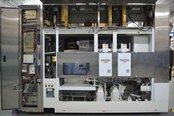
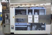
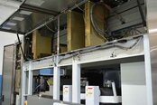
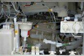
Used SEMITOOL Paragon #293592805 for sale
URL successfully copied!
Tap to zoom
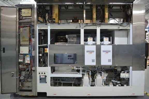

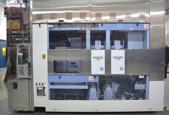

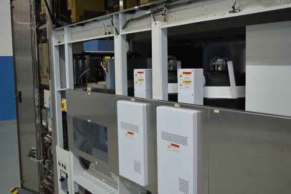

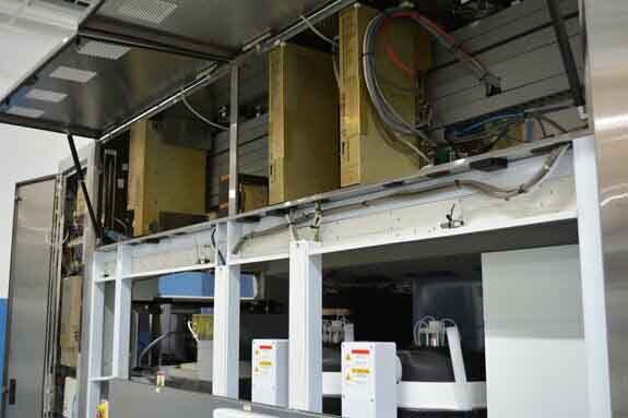

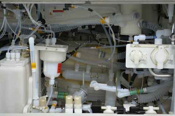


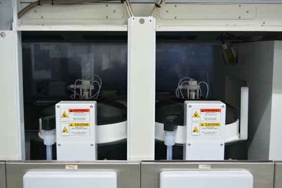

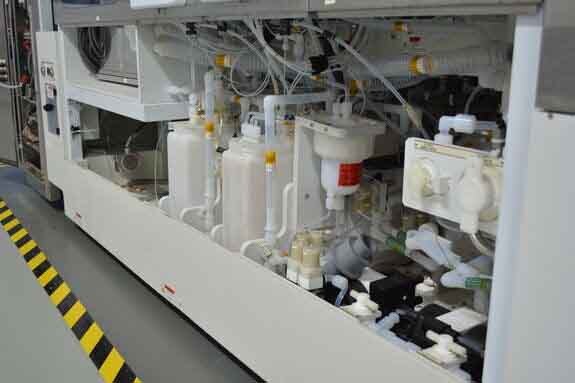

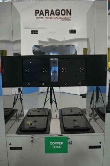

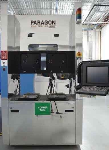

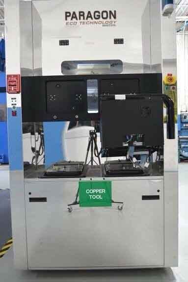

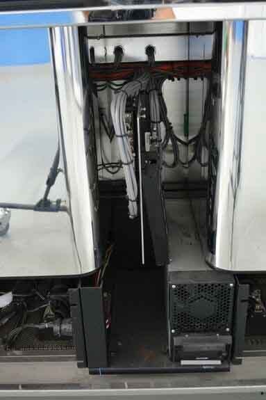

ID: 293592805
Wafer Size: 12"
ECD Plating system, 12"
(2) FOUP WIP
Anneal chamber
ULVAC Metrology unit
(2) CFD Chambers with in-situ rinse
RTA Probe
Pump
Bleed bath recovery
(2) Capsule chambers with cooling coils
Heated N2
Sample port
Tank with AMCS connections
Power supply: 480 VAC, 125 A, 50/60 Hz.
SEMITOOL Paragon is a 'photoresist' equipment developed by SEMITOOL, Inc. for creating extremely fine features in semiconductors. The system utilizes a high-precision mask-aligner that is capable of imaging patterns onto a semiconductor substrate with outstanding accuracy. The process starts with a photomask containing the pattern that needs to be transferred onto the substrate. Then, a specialized piece of photomask is placed above the substrate, and light shining through the mask is used to create the desired pattern. Paragon photoresist unit is composed of two main pieces of equipment: the Photo Aligner and the Developer. The Photo Aligner is composed of an alignment stage, a top-holder, and an illuminator. The alignment stage controls the precision with which the photomask is aligned over the substrate, while the top-holder provides a smooth surface that the photomask can move over. The illuminator utilizes photoresist-compatible light sources, including visible, UV and IR, to allow for the creation of extremely fine features. The Developer is designed for the removal and fixation of the photoresist material. After the photoresist material has been exposed to the desired pattern, it must be cleaned from the surface and a new layer of photoresist needs to be applied. To achieve this, the Developer utilizes a wet bench which uses chemical baths to remove and fix the photoresist. SEMITOOL Paragon photoresist machine is designed to enable the accurate and repeatable creation of semiconductor patterns with small sizes and feature sizes. The tool provides accuracy down to 45nm with high throughput and feature-size control. The asset's mask-aligner allows for extremely precise alignment of the photomask on the wafer to further increase accuracy. Additionally, the model allows for the use of a variety of photoresists, ensuring that the desired feature sizes can be achieved.
There are no reviews yet
