Used SEMITOOL Raider ECD 212 #293807056 for sale
URL successfully copied!
























Tap to zoom
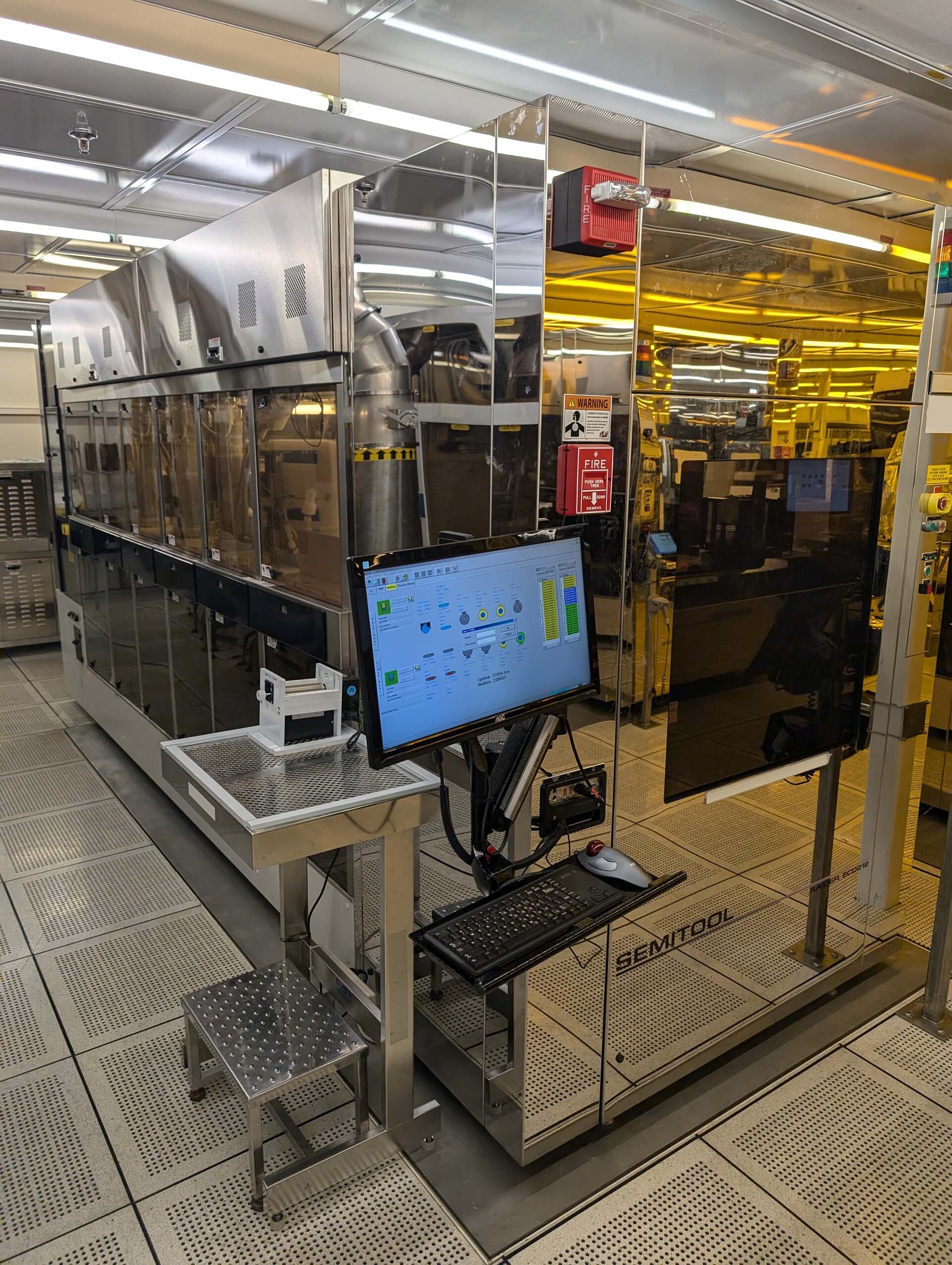

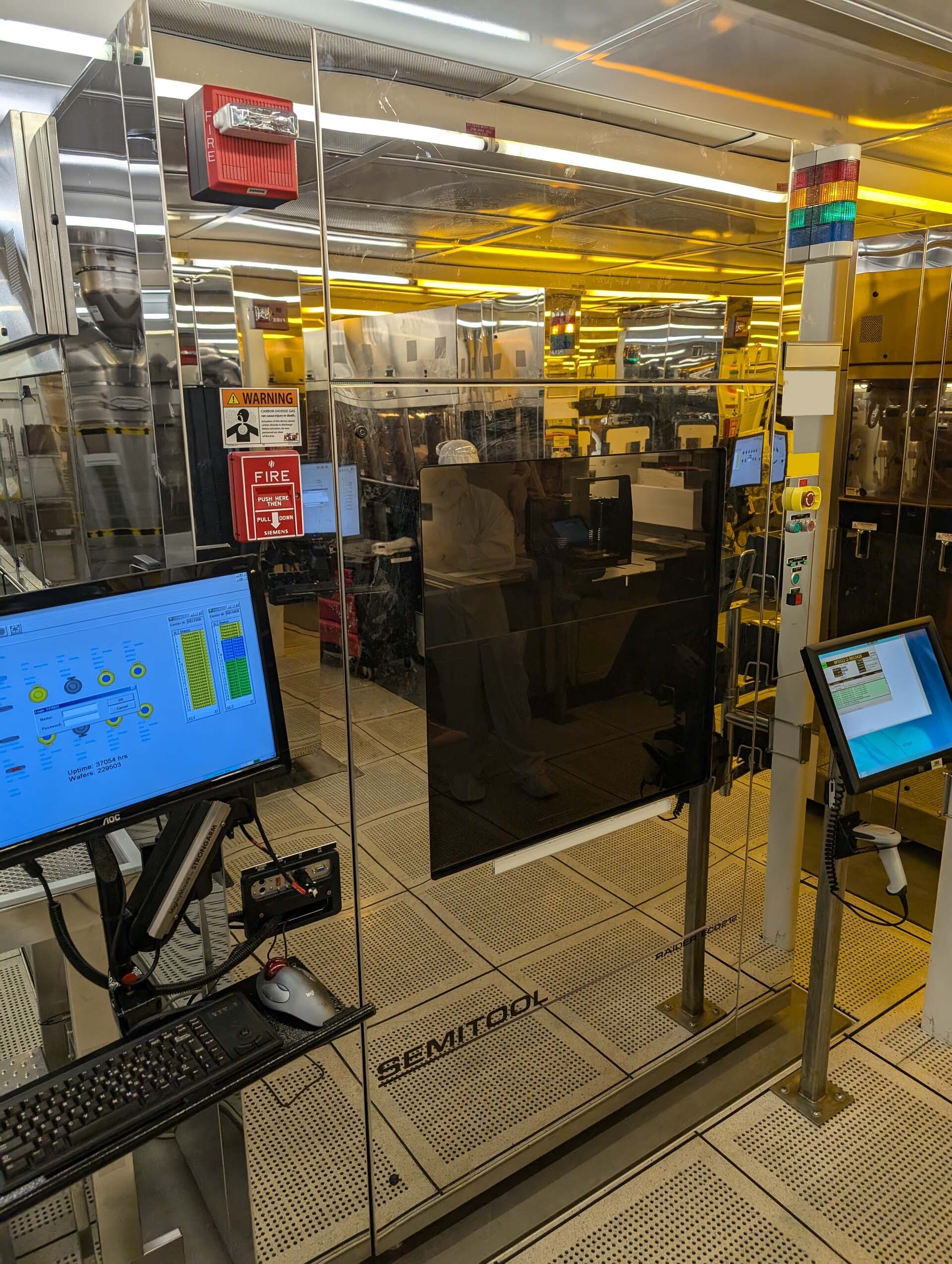
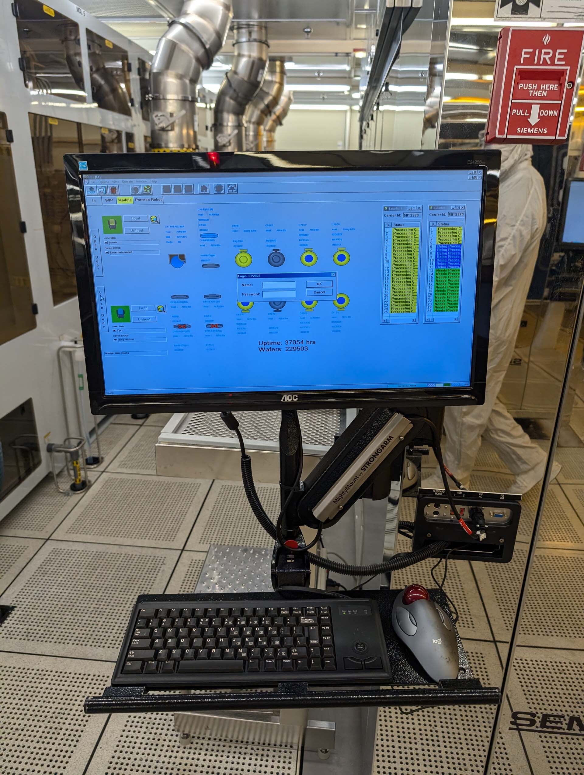
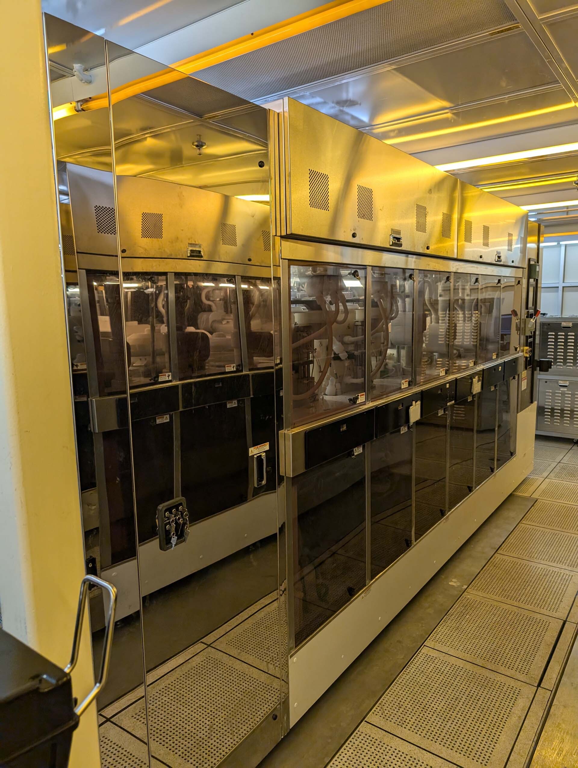
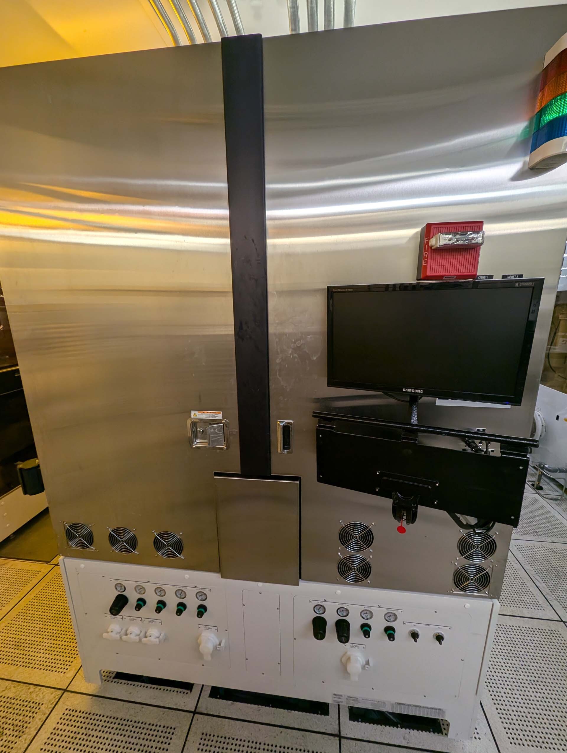
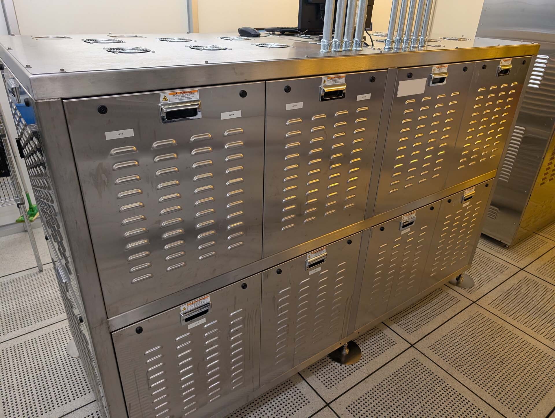
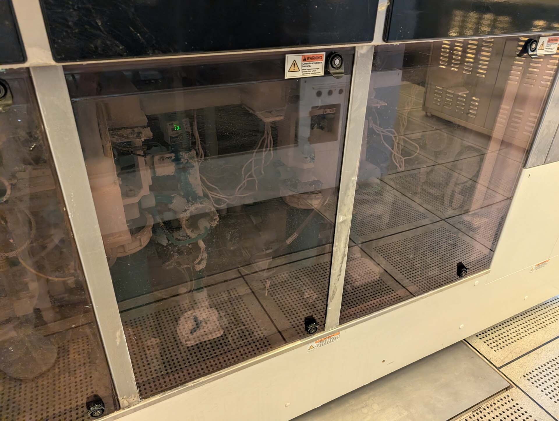
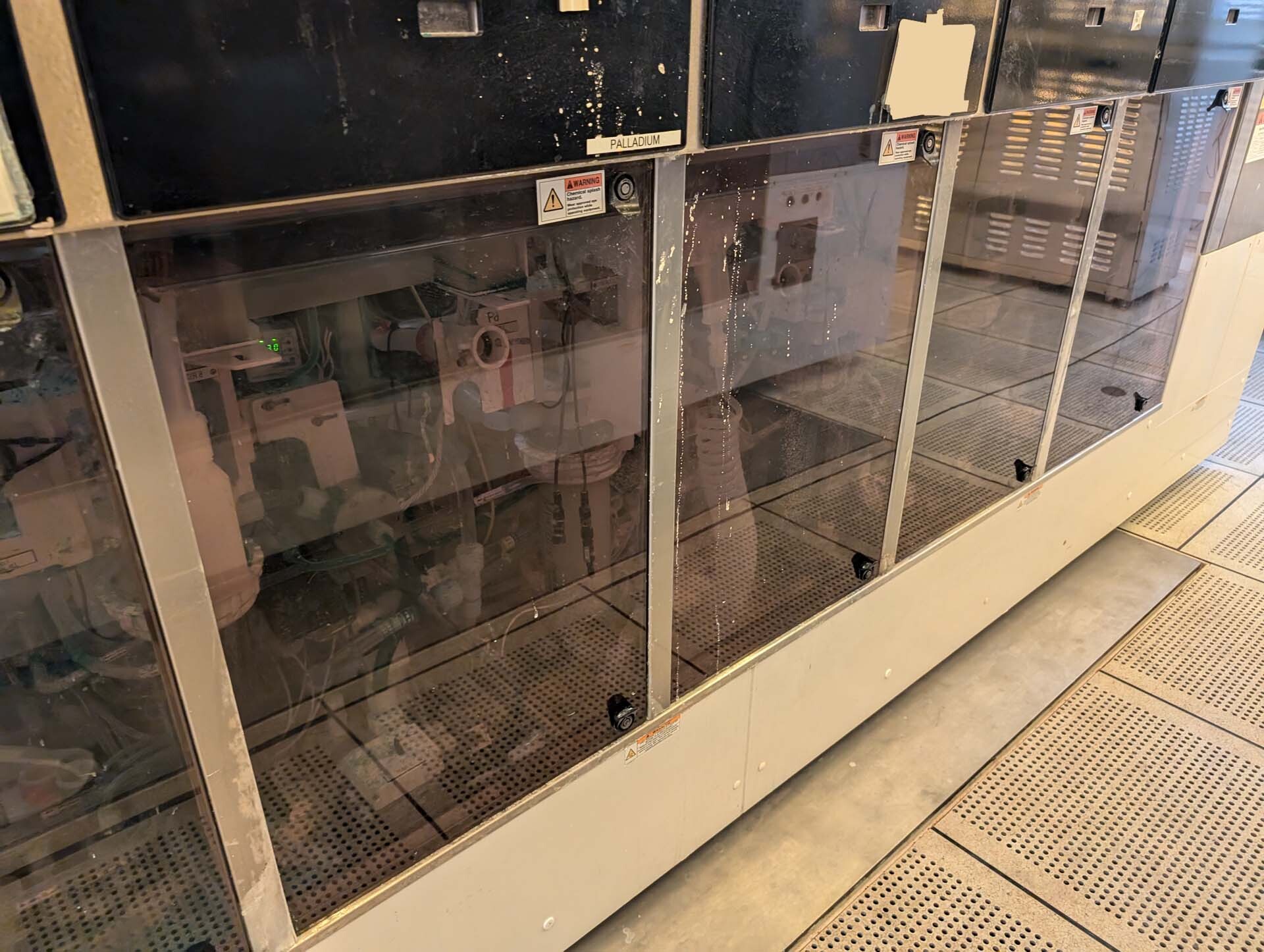
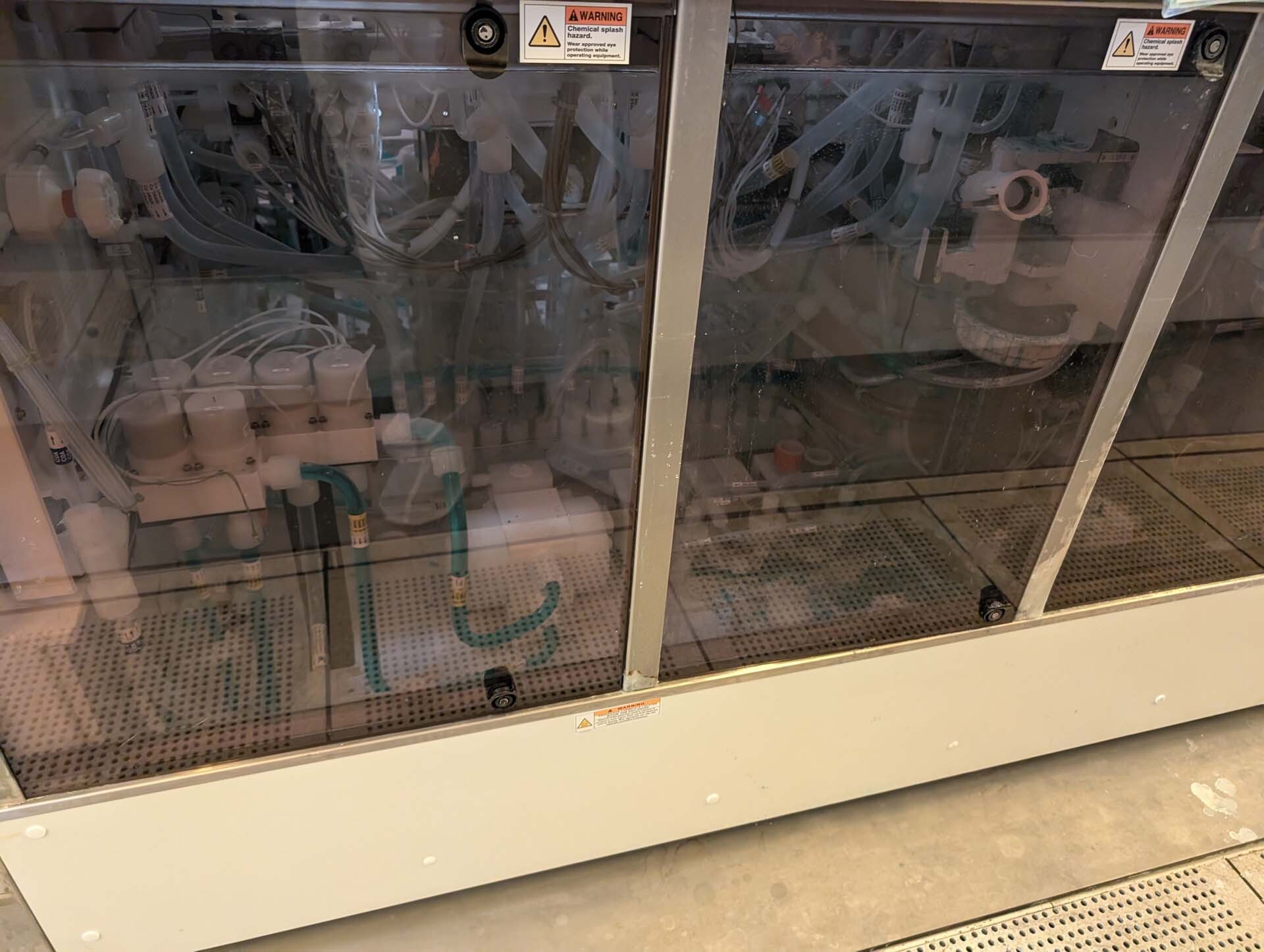
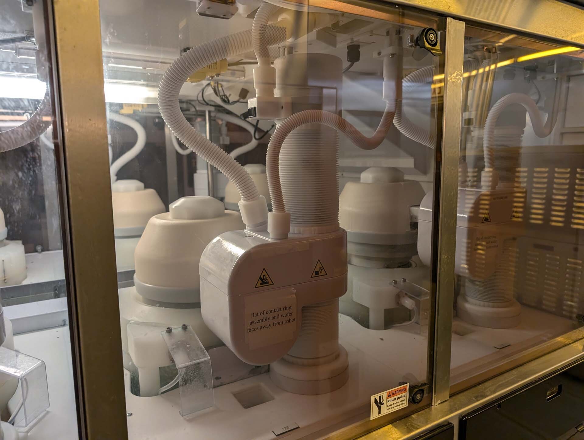
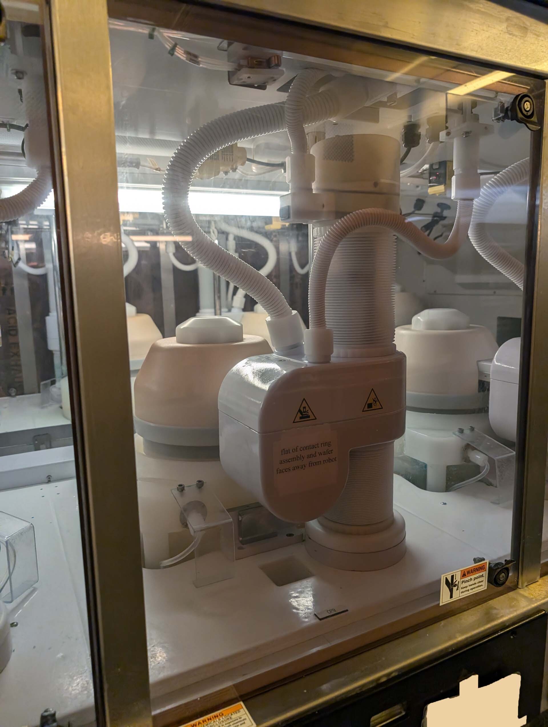
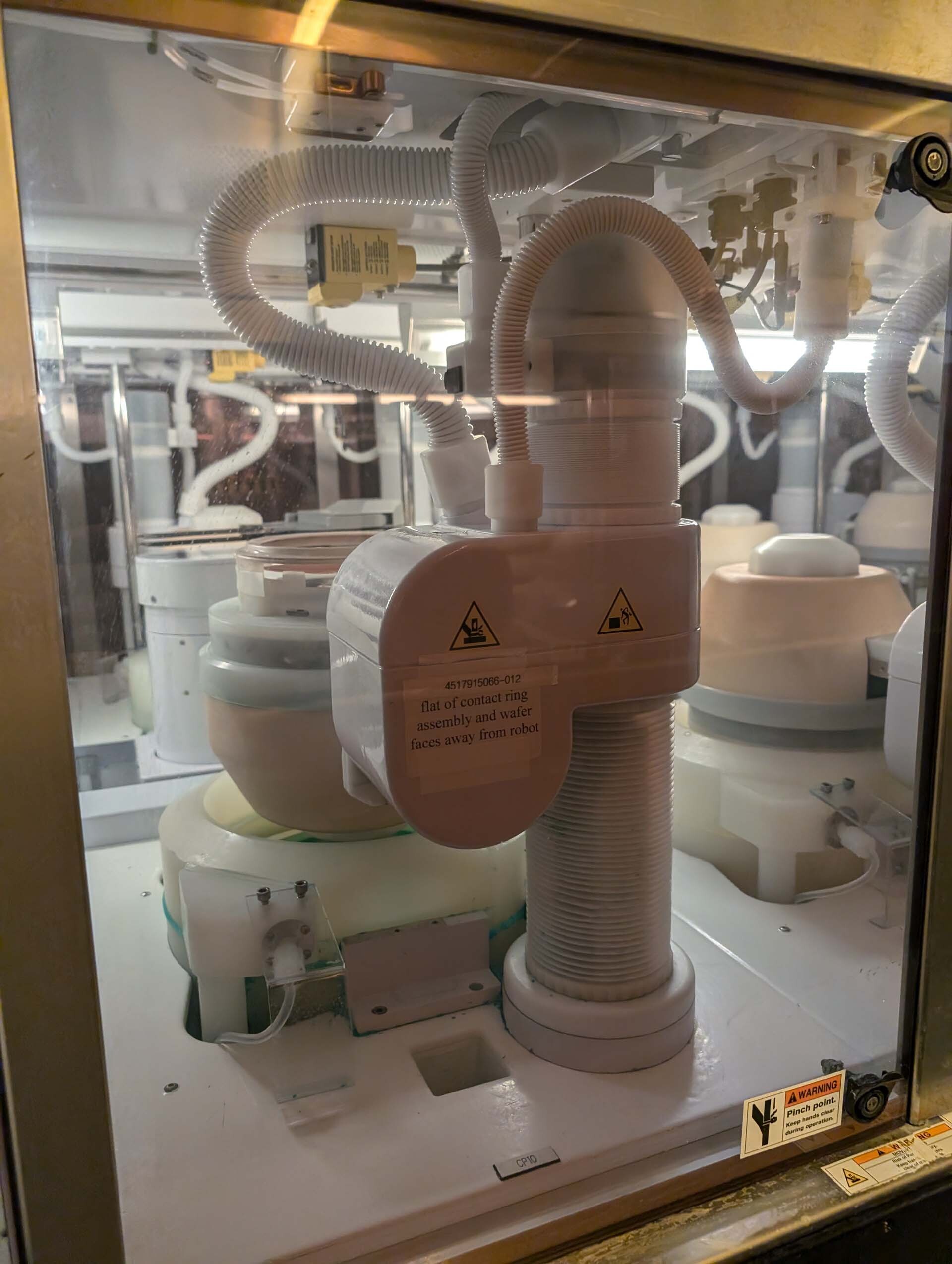
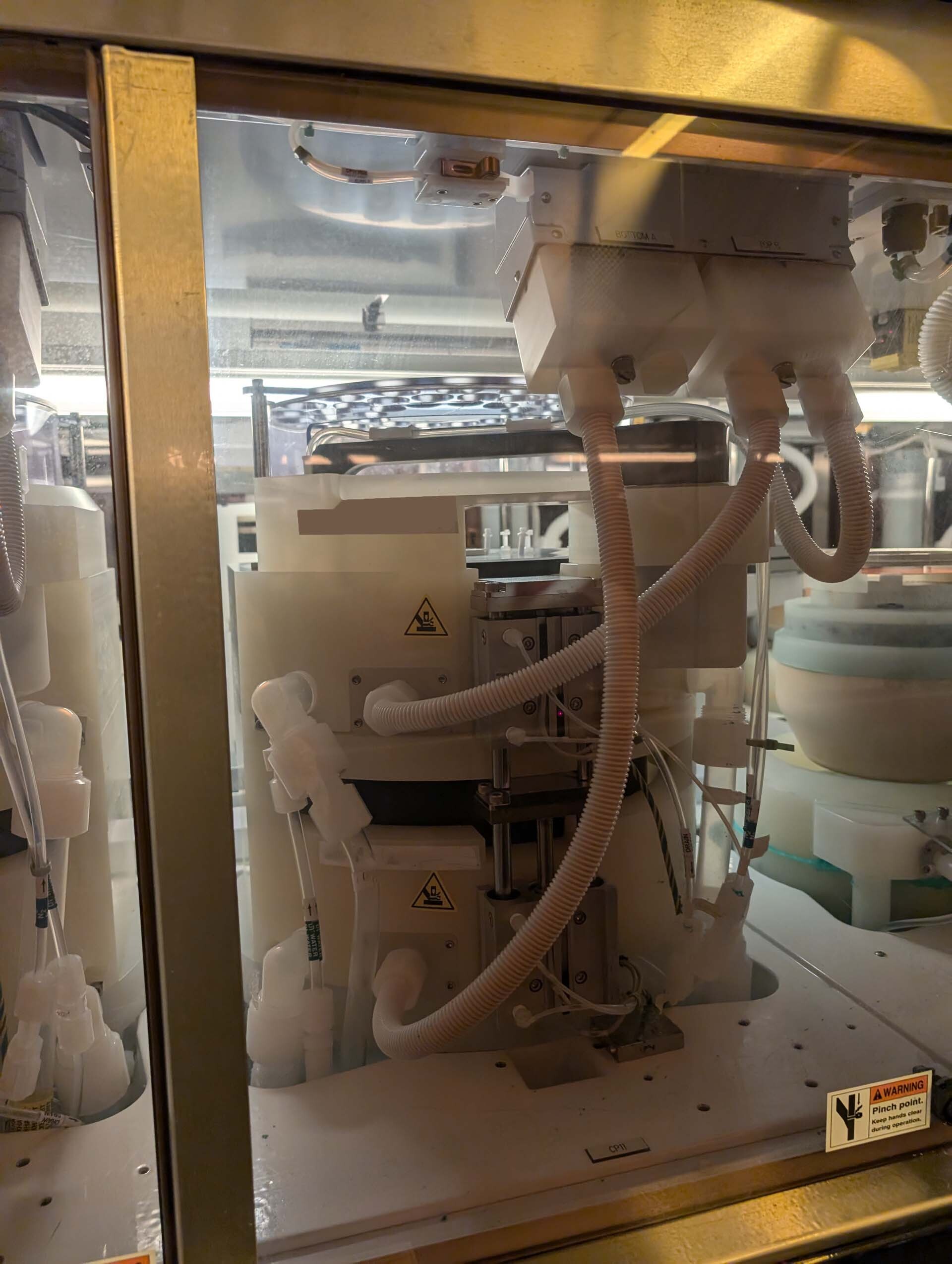
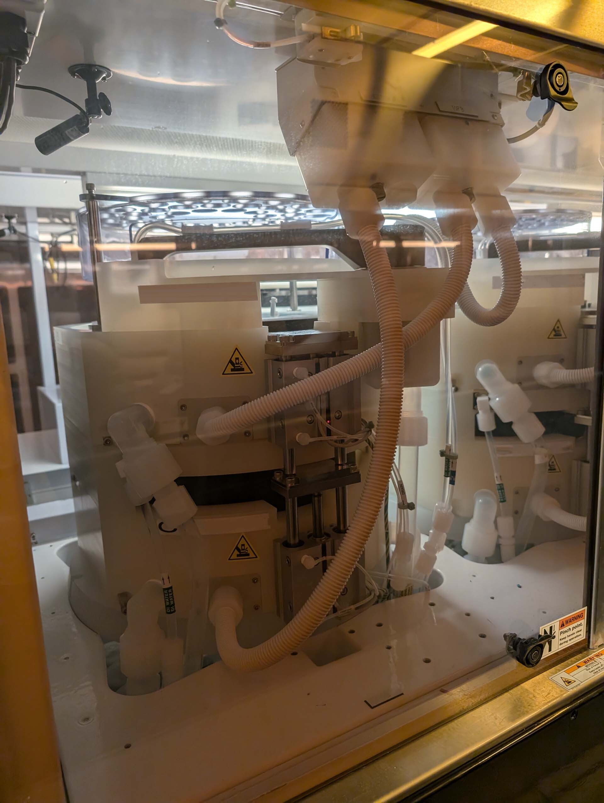
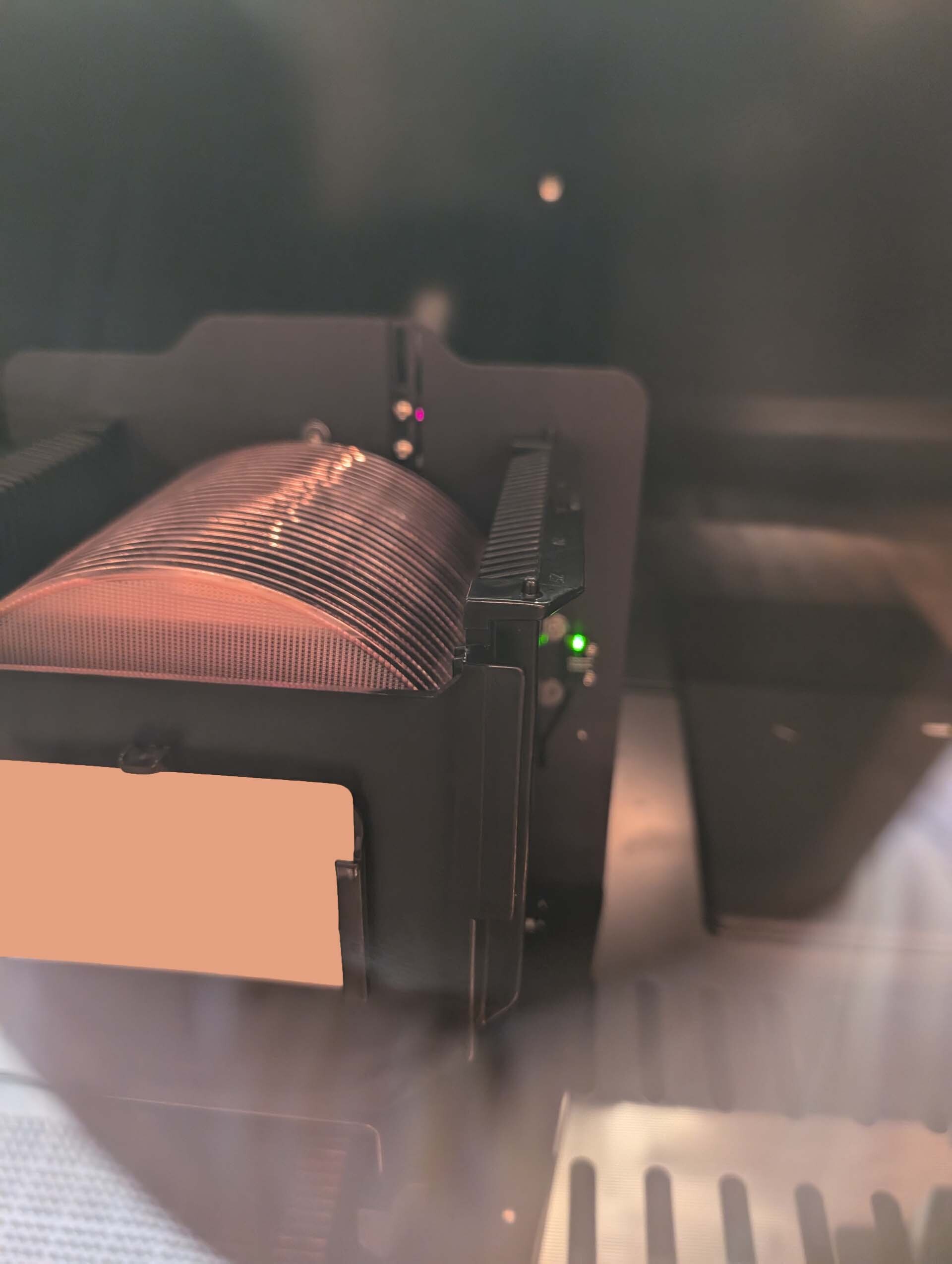
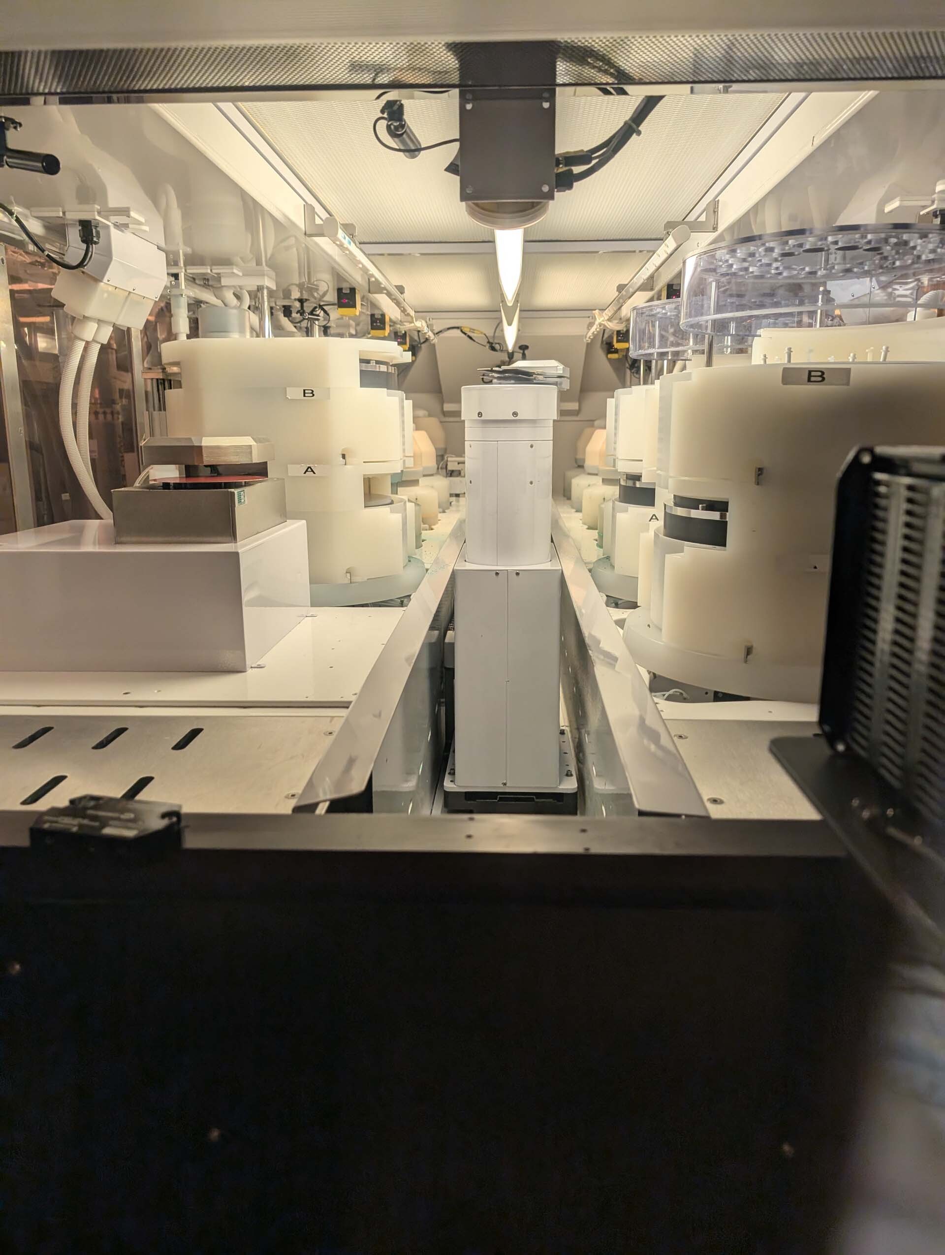
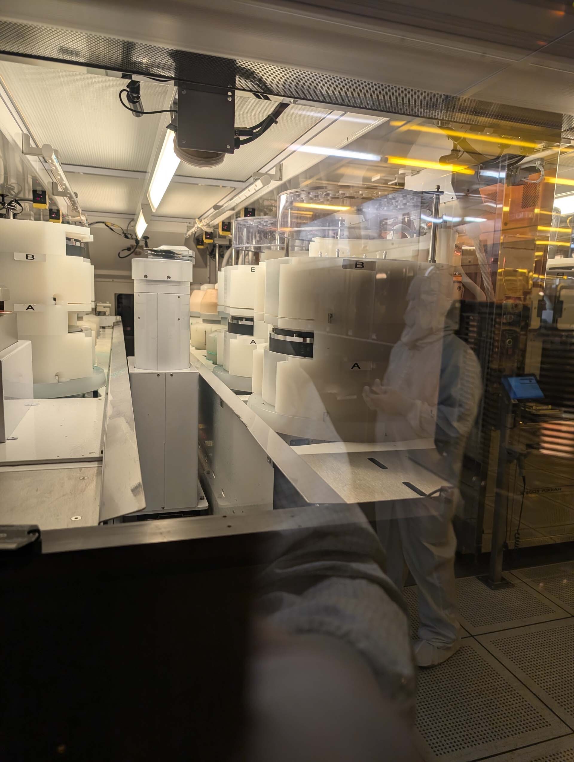
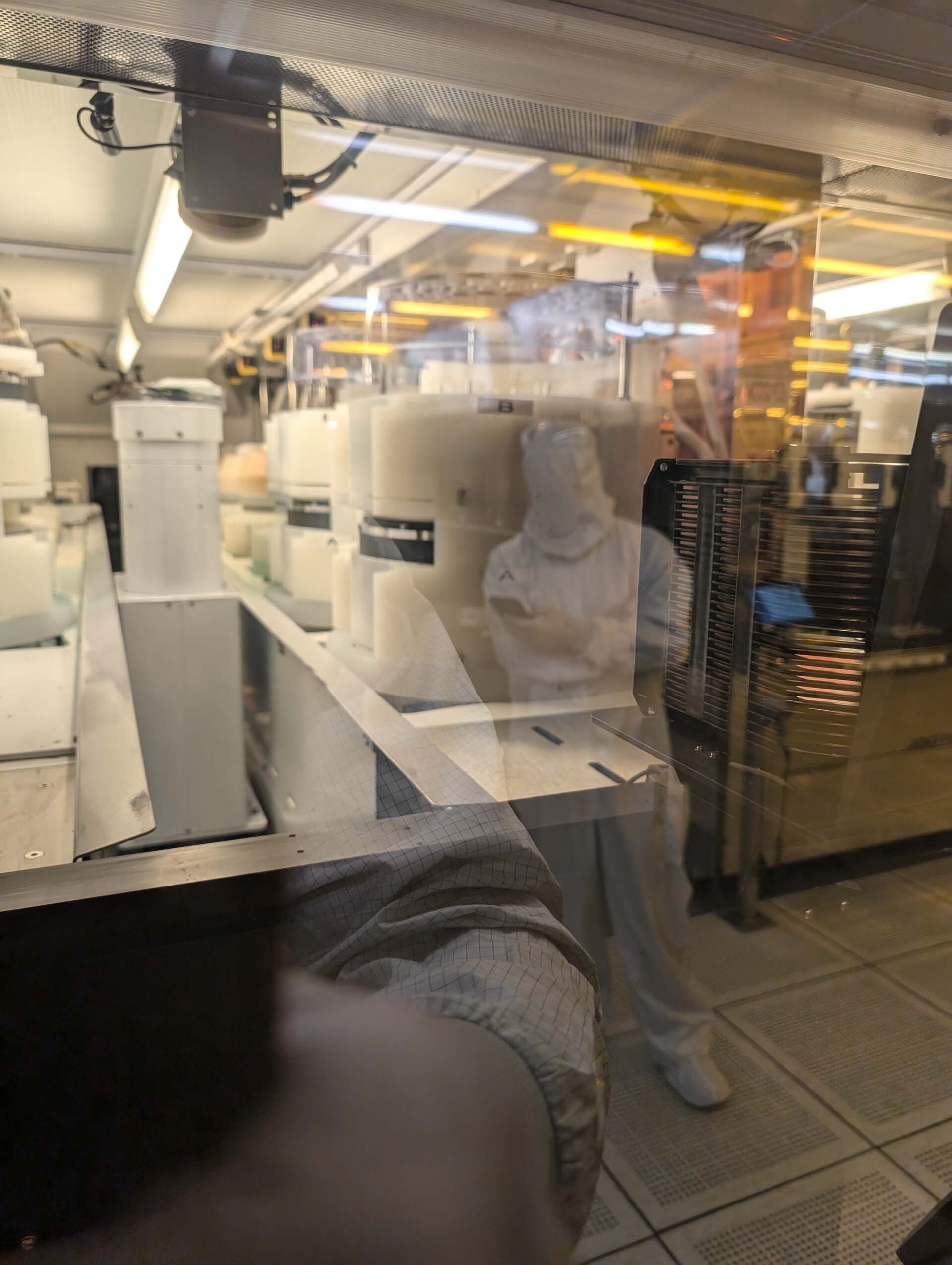
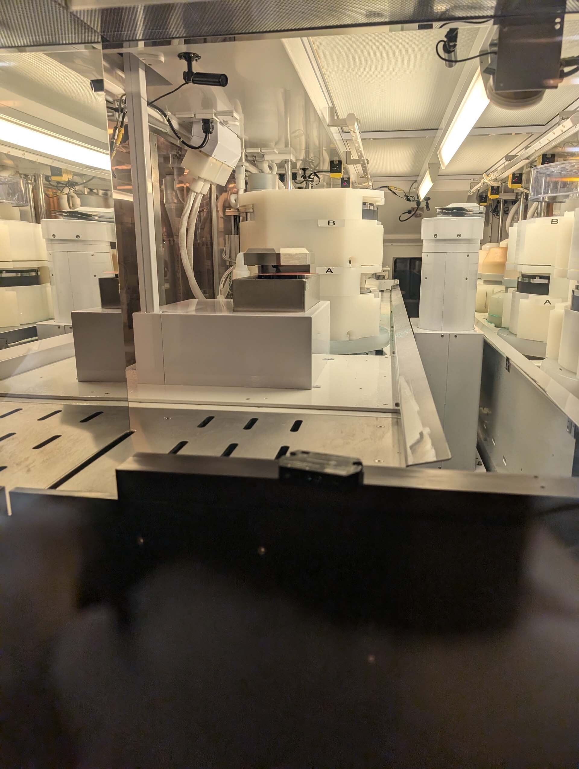
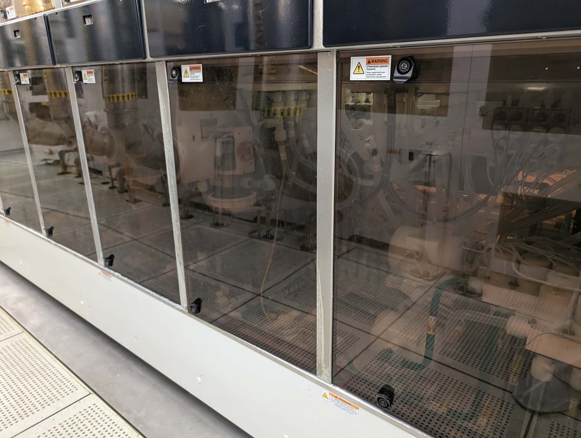
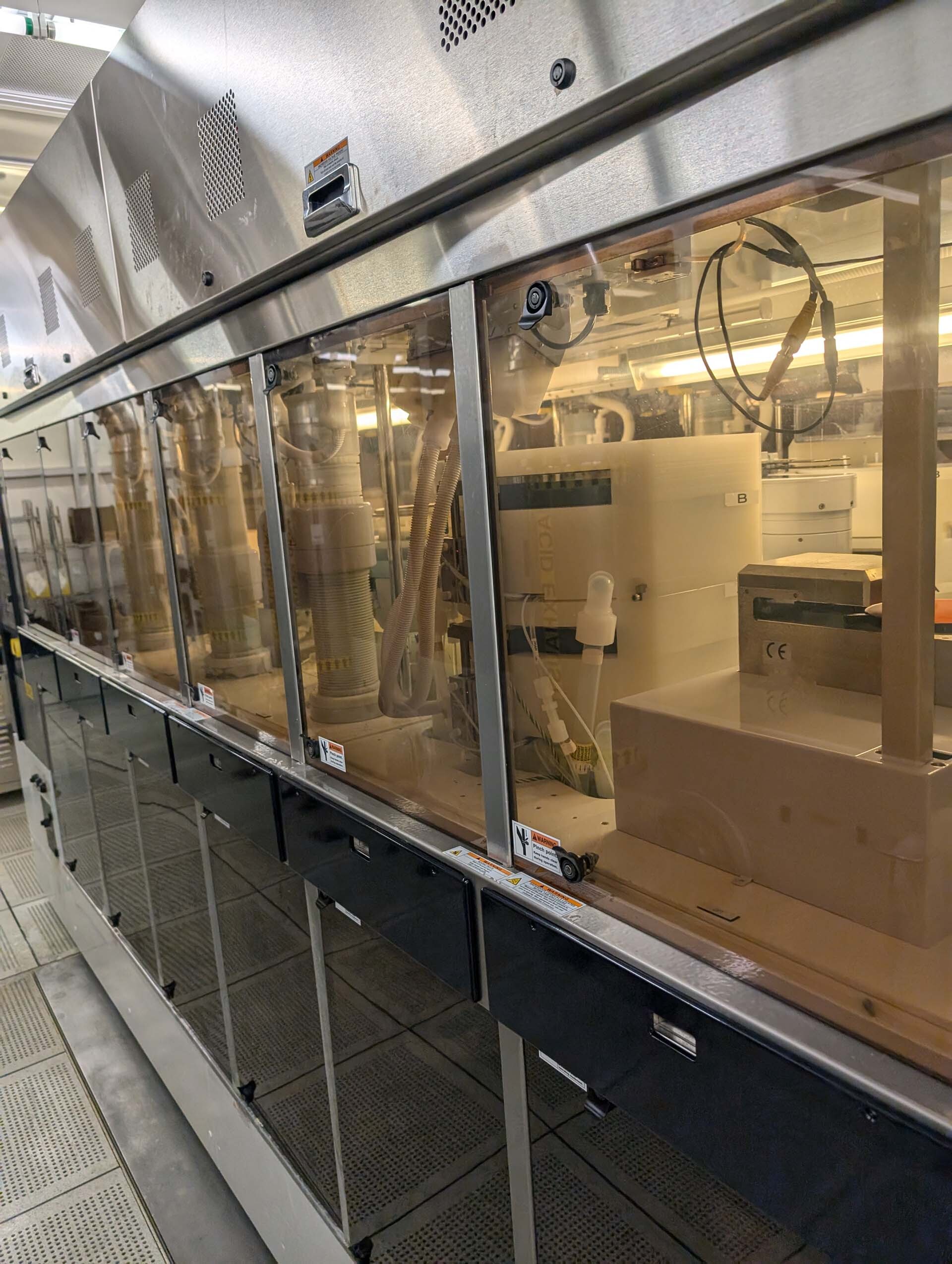
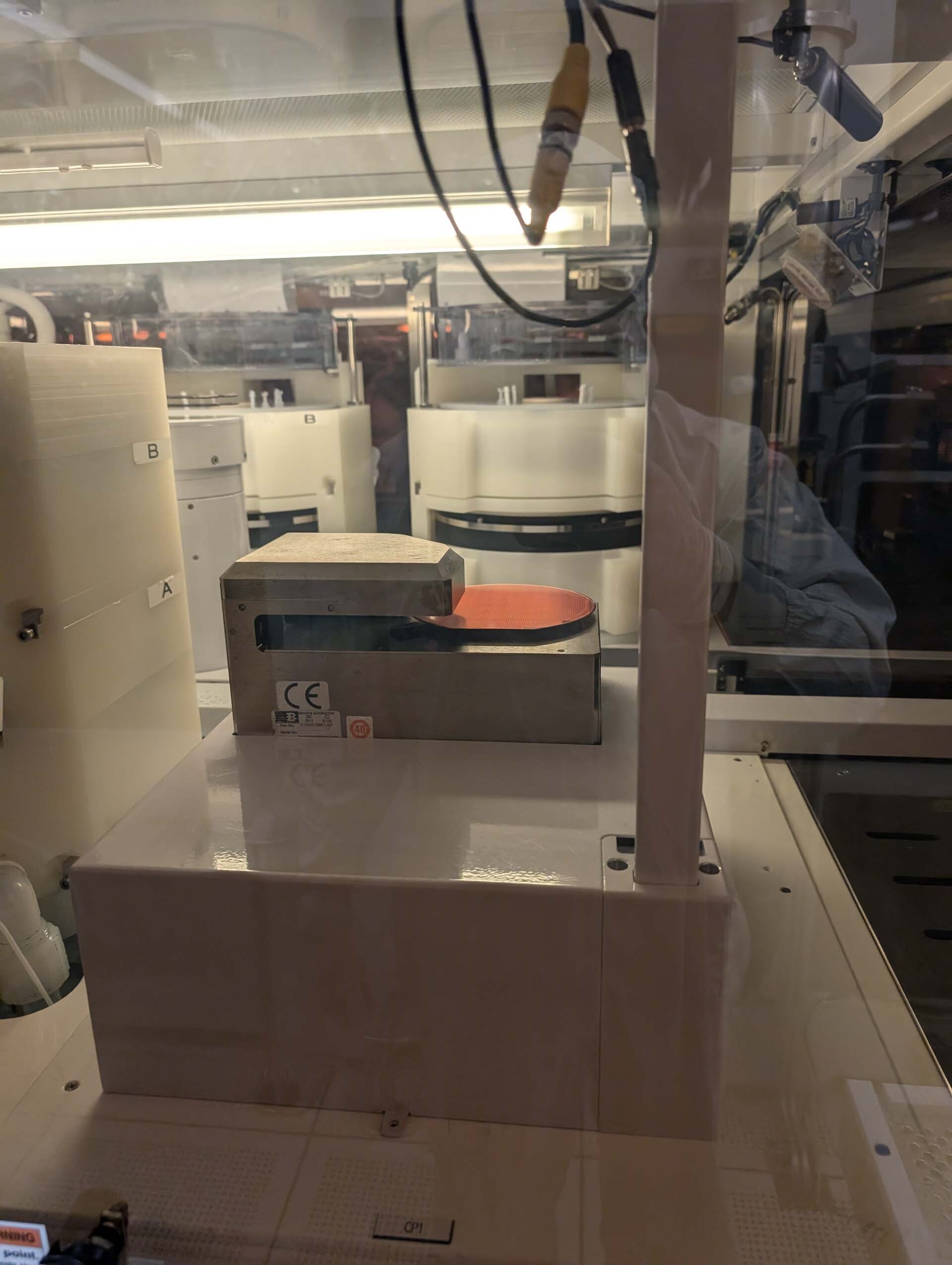
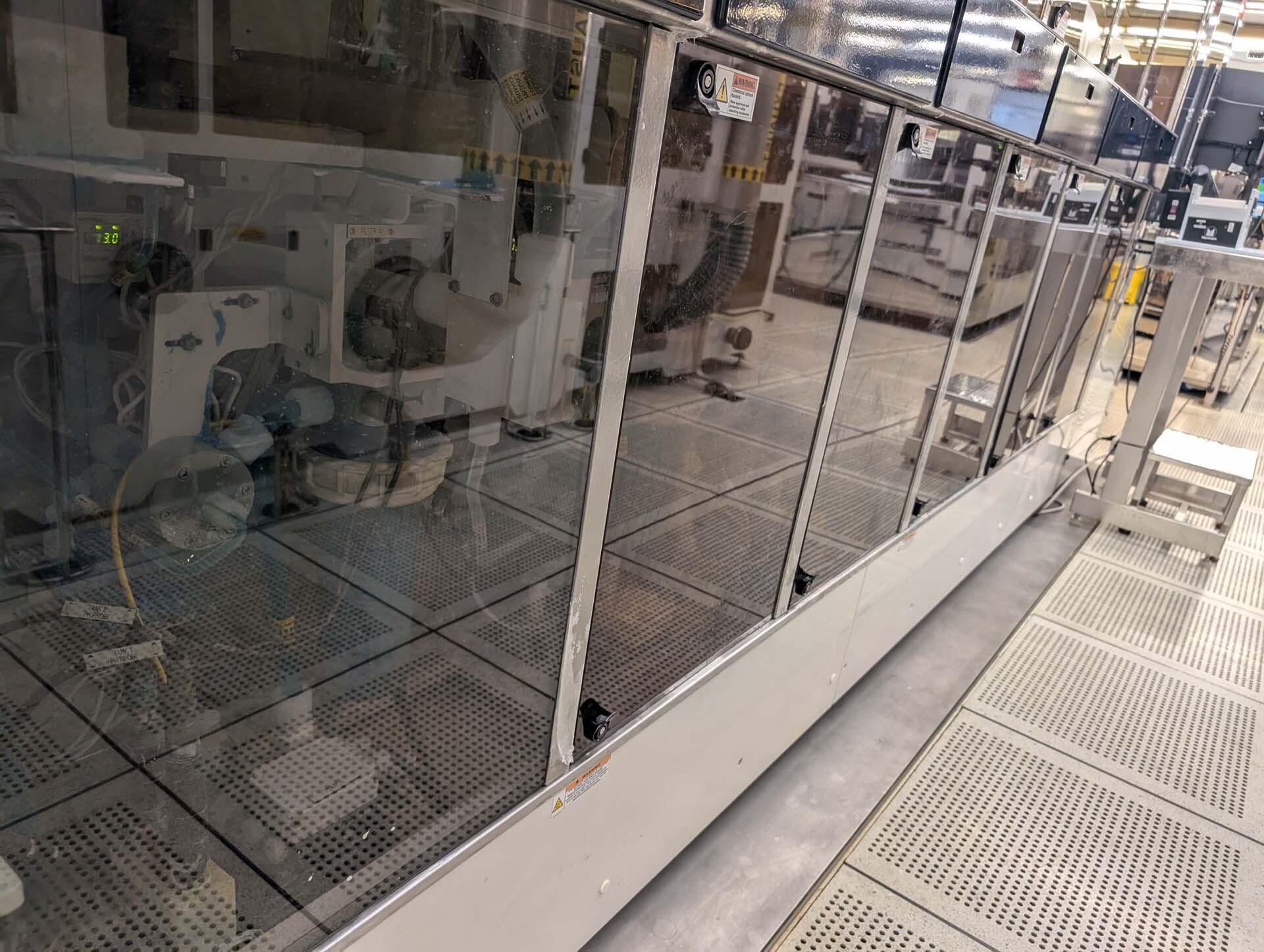
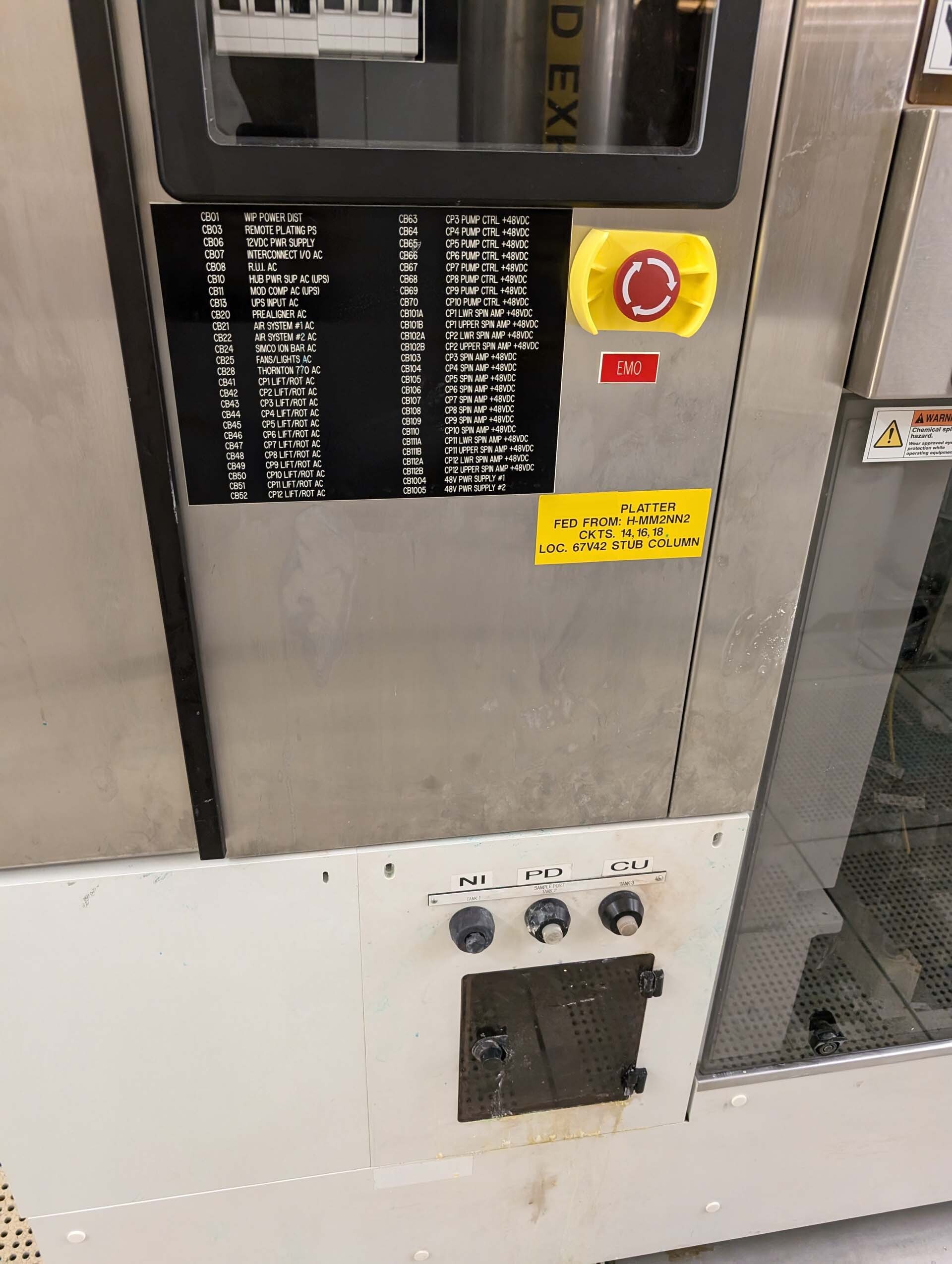
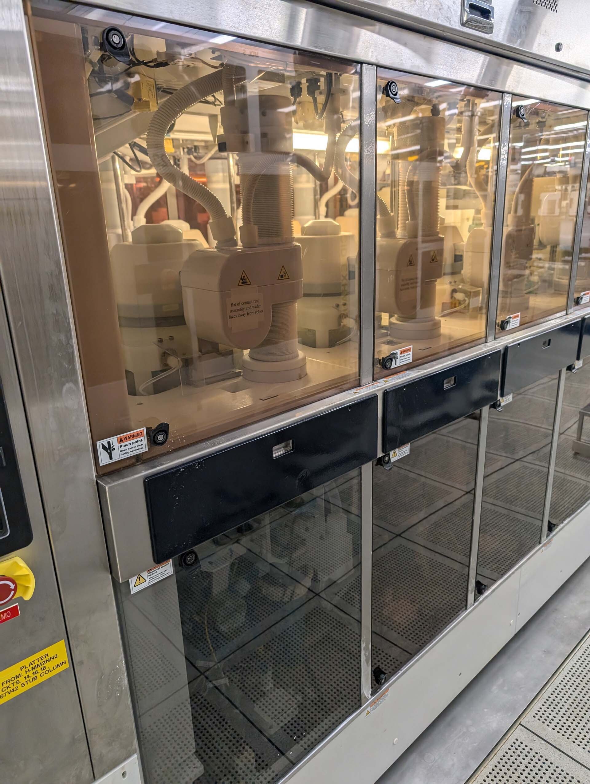
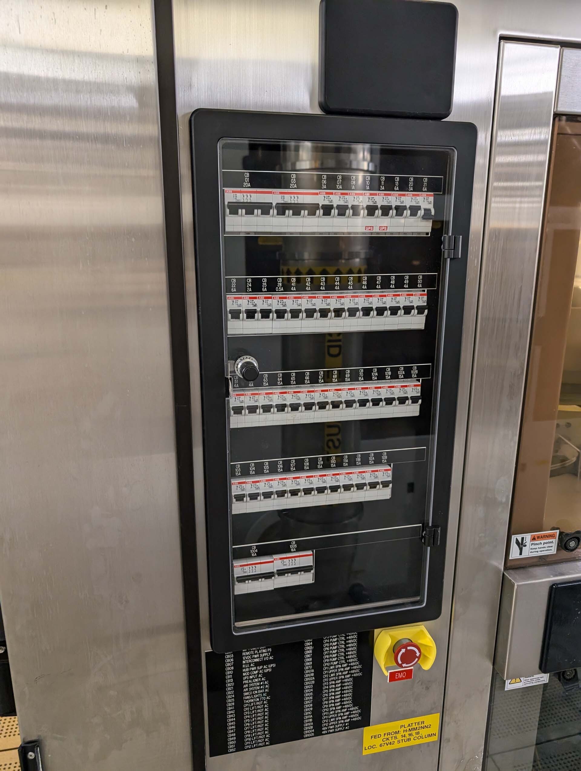
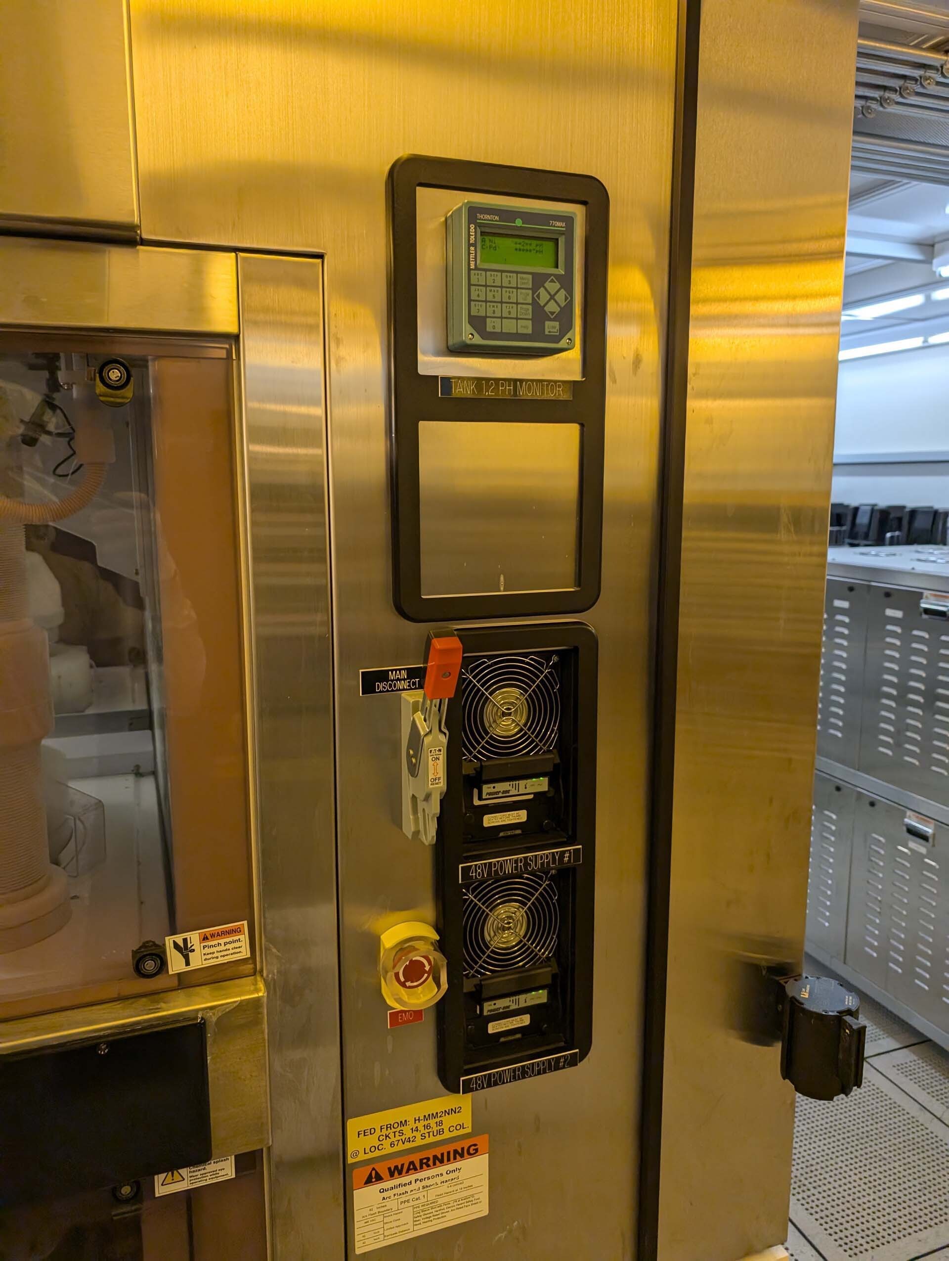

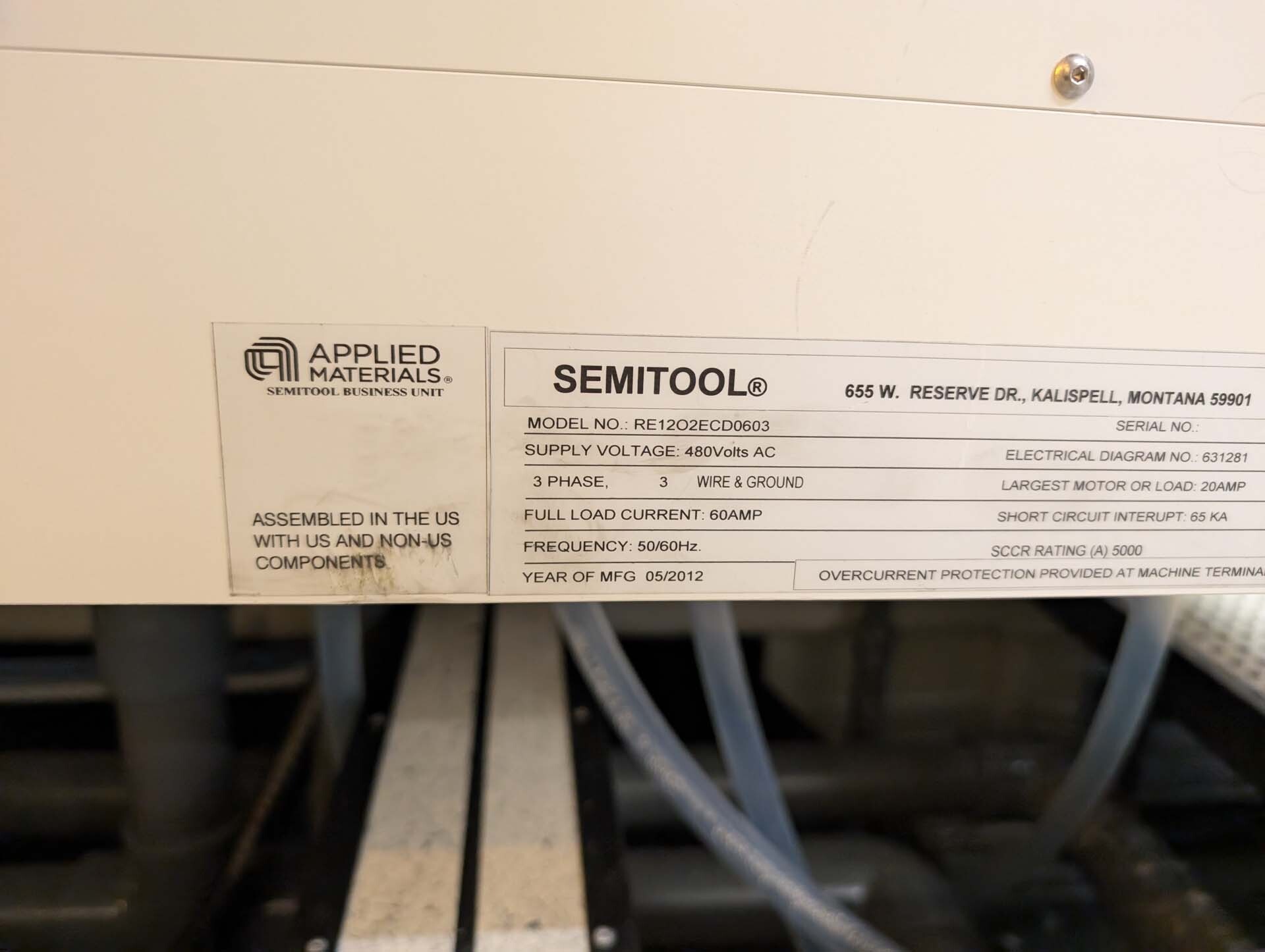
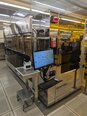
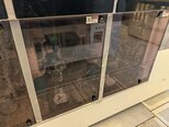
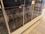
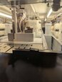
SEMITOOL Raider ECD 212 is a highly advanced photoresist equipment designed for semiconductor manufacturing processes. This system offers cutting-edge technology to provide precise and efficient photoresist coating and development for semiconductor wafers. Raider ECD 212 is equipped with state-of-the-art features that enable high-performance results in the fabrication of integrated circuits and other semiconductor devices. At the core of SEMITOOL Raider ECD 212 is its ElectroChemical Deposition (ECD) technology, which is crucial for achieving uniform and controlled deposition of photoresist material on wafers. The ECD process utilizes electrochemical reactions to deposit photoresist layers with high precision and consistency, ensuring uniform coverage across the entire wafer surface. This technology allows for the creation of intricate patterns and structures on semiconductor wafers with minimal variation and defects. One of the key features of Raider ECD 212 is its advanced automation capabilities, which streamline the photoresist coating and development processes. The unit is equipped with a robotic arm that can handle multiple wafers simultaneously, allowing for high-throughput production with minimal manual intervention. This automation not only speeds up the manufacturing process but also reduces the potential for errors and contamination, resulting in higher yields and lower production costs. SEMITOOL Raider ECD 212 is also equipped with a sophisticated control machine that enables precise adjustment of process parameters such as deposition rate, film thickness, and curing time. Operators can easily program and monitor these parameters through an intuitive interface, allowing for real-time monitoring of the deposition process and quick adjustments as needed. This level of control ensures that the photoresist layers are deposited with the desired characteristics and properties, meeting the strict requirements of semiconductor fabrication. In addition to its advanced technology and automation capabilities, Raider ECD 212 is designed for versatility and flexibility in accommodating various semiconductor wafer sizes and types. The tool can support wafer sizes ranging from small to large diameters, and it is compatible with a wide range of photoresist materials commonly used in semiconductor fabrication. This flexibility makes SEMITOOL Raider ECD 212 suitable for a variety of applications in the semiconductor industry, from research and development to high-volume production. Furthermore, Raider ECD 212 is engineered for reliability and durability, with robust construction and high-quality components that ensure consistent performance over extended periods of operation. The asset is designed to meet the demanding requirements of semiconductor manufacturing environments, with features such as advanced filtration systems to maintain the purity of process chemicals and prevent contamination. These design elements contribute to the model's overall efficiency and reliability, making it a trusted solution for semiconductor manufacturers worldwide. Overall, SEMITOOL Raider ECD 212 is a cutting-edge photoresist equipment that offers unparalleled performance, precision, and reliability in semiconductor manufacturing. With its advanced technology, automation capabilities, and versatility, Raider ECD 212 is a valuable tool for achieving high-quality results in the fabrication of semiconductor devices, contributing to the advancement of technology in various industries.
There are no reviews yet