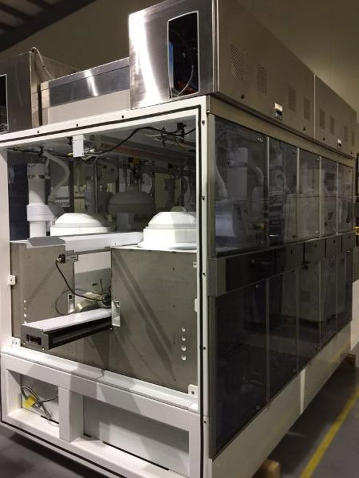
Used SEMITOOL Raider ECD 310 #9274916 for sale
URL successfully copied!
Tap to zoom


SEMITOOL Raider ECD 310 is an advanced photoresist equipment developed for stabilization of high quality photoresist circuitry patterns in microelectronics production. It provides improved performance that exceeds the capabilities of standard lithographic methods. The equipment utilizes advanced direct write technology, which avoids costly contact printing of resist patterns while maintaining the highest image quality and precision. This system features a monochrome laser alignment unit that utilizes laser diodes in place of traditional optical components, enabling superior accuracy. This technology also eliminates misalignments and compensates for shot-to-shot process variation throughout a production run, guaranteeing consistent etch depth and a reliable etch rate. SEMITOOL RAIDER ECD-310 is backed by an array of features that make it an attractive choice for photoresist processing. It has a high power capability and provides an efficient proces rcor potential of up to 36V. The machine also has an advanced protective coating layer, which reduces the possibility of adhesion plate damage from heat and aggressive chemicals. It features a compact design which enables efficient fabrication space while offering the highest throughput and reliability. Raider ECD 310 also provides temperature controlling capabilities that guarantee particle-free process and cooling processes. This tool is equipped with a high-performance megasonic cleaning unit which utilizes megasonic waves to compound into the photoresist layer above the patterned device. This cleaning process offers consistent results and excellent precision. In addition, the asset also features a low-temperature bake furnace, rapid solvent dryer and encapsulated developer. These components work together to provide an accurate process result without incurring additional thermal damage. RAIDER ECD-310 is capable of creating intricate circuitry patterns with feature sizes as small as 2µm, providing superior resolution for the most demanding applications. It is an effective and reliable tool for today's microelectronics manufacturing environment due to its advanced technological features, allowing for efficient fabrication of complex photoresist circuitry patterns.
There are no reviews yet