Used SEMITOOL Raider ECD 312 #293807054 for sale
URL successfully copied!










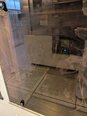



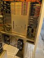

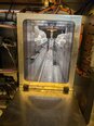
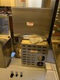










Tap to zoom
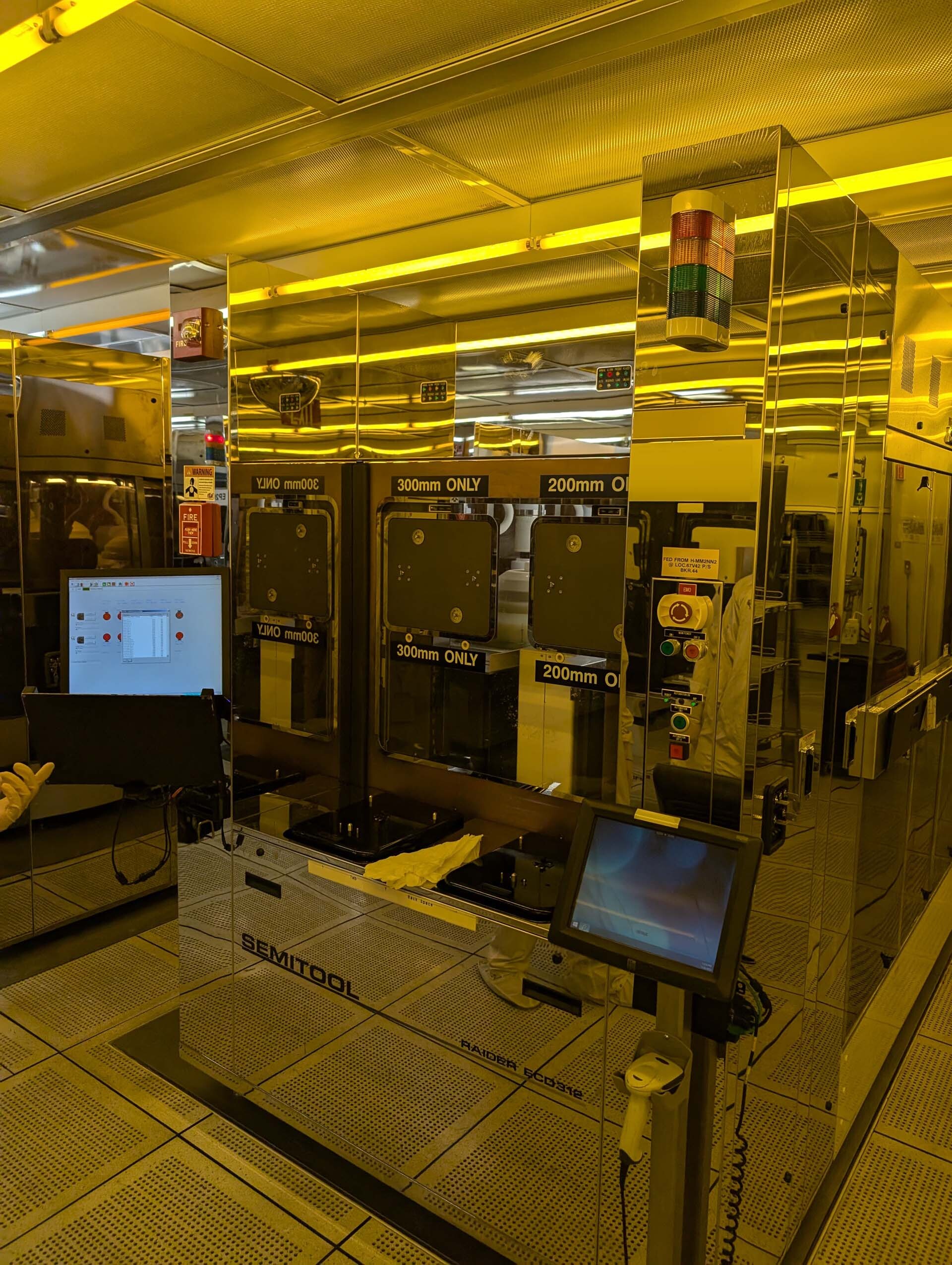

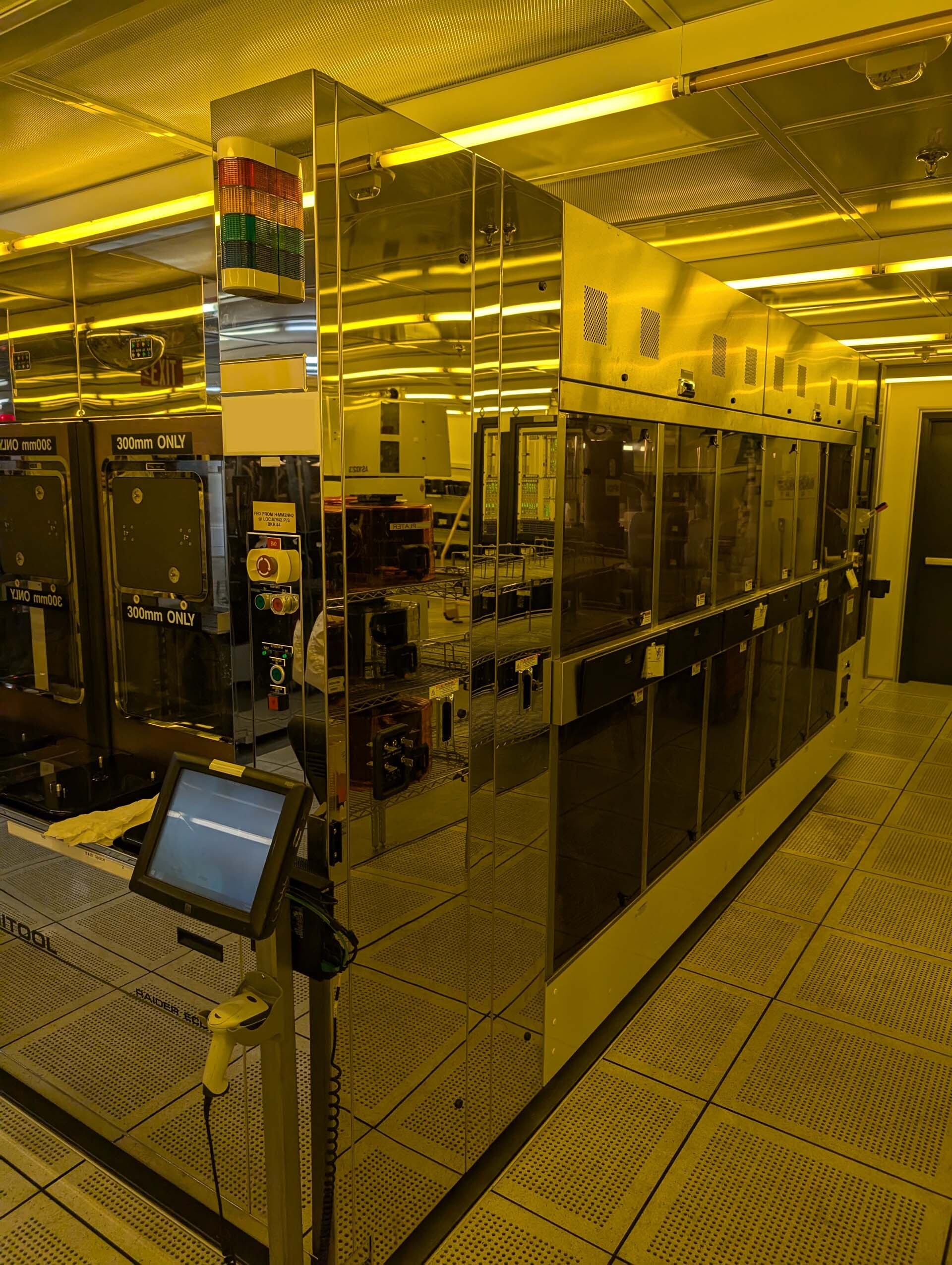
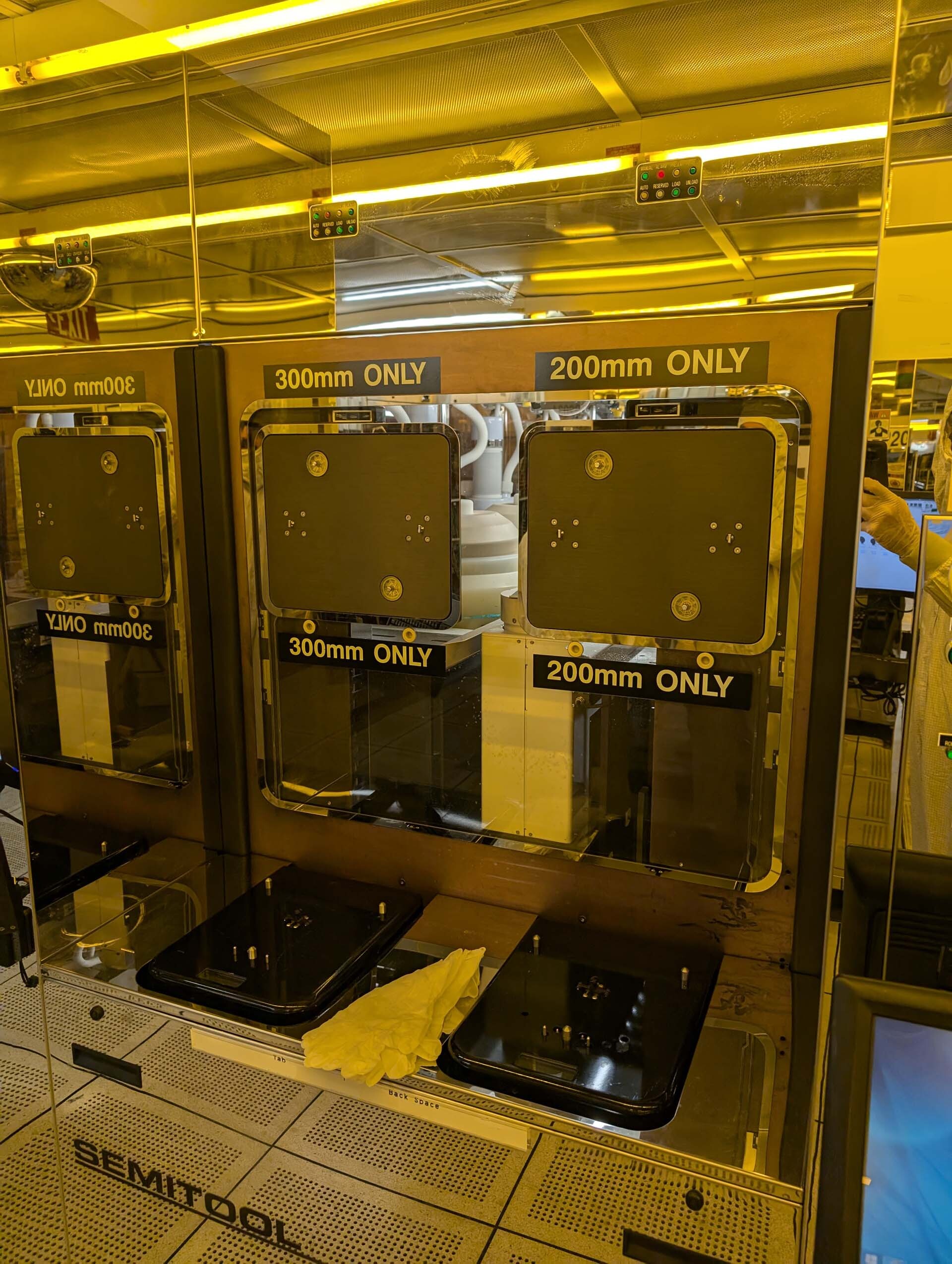
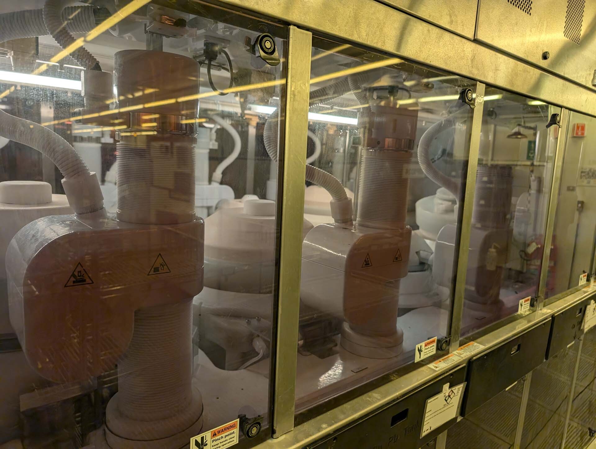
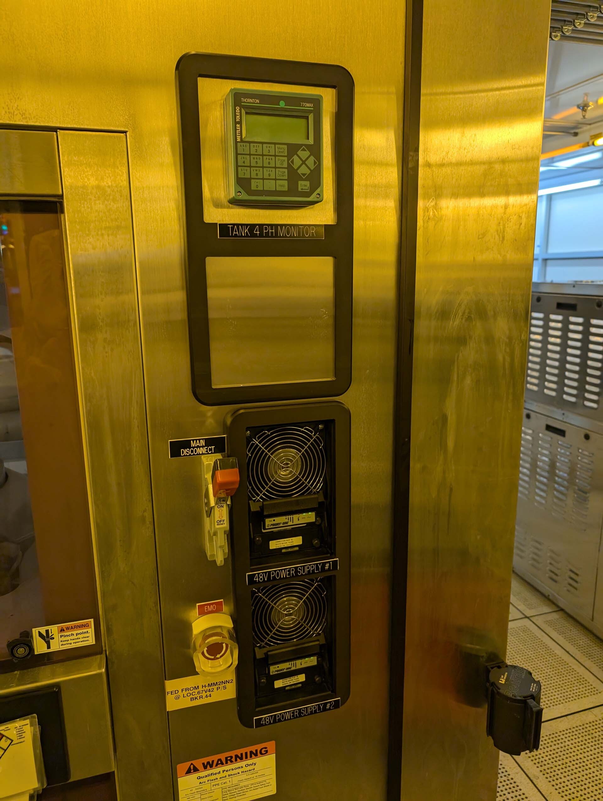
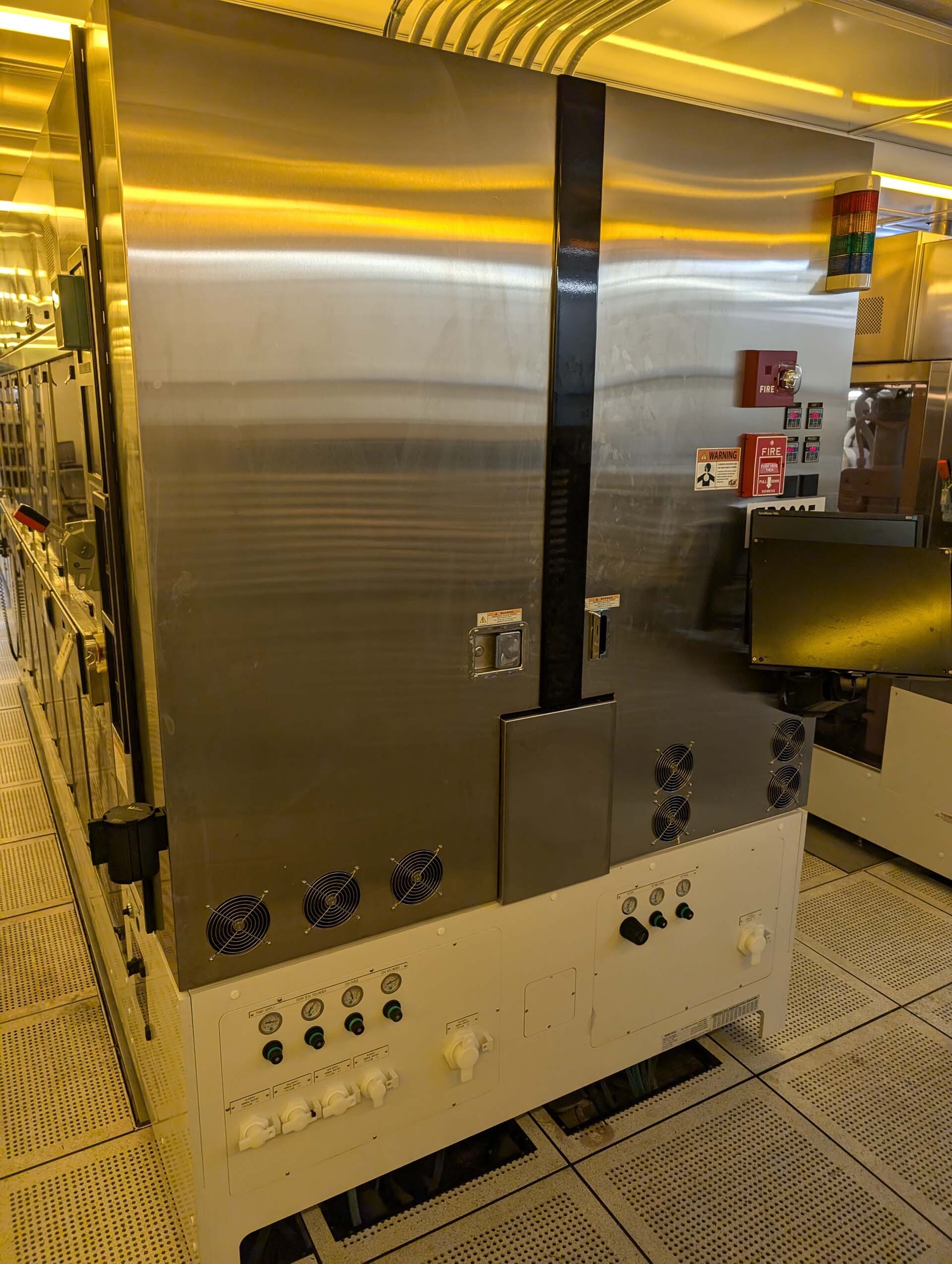
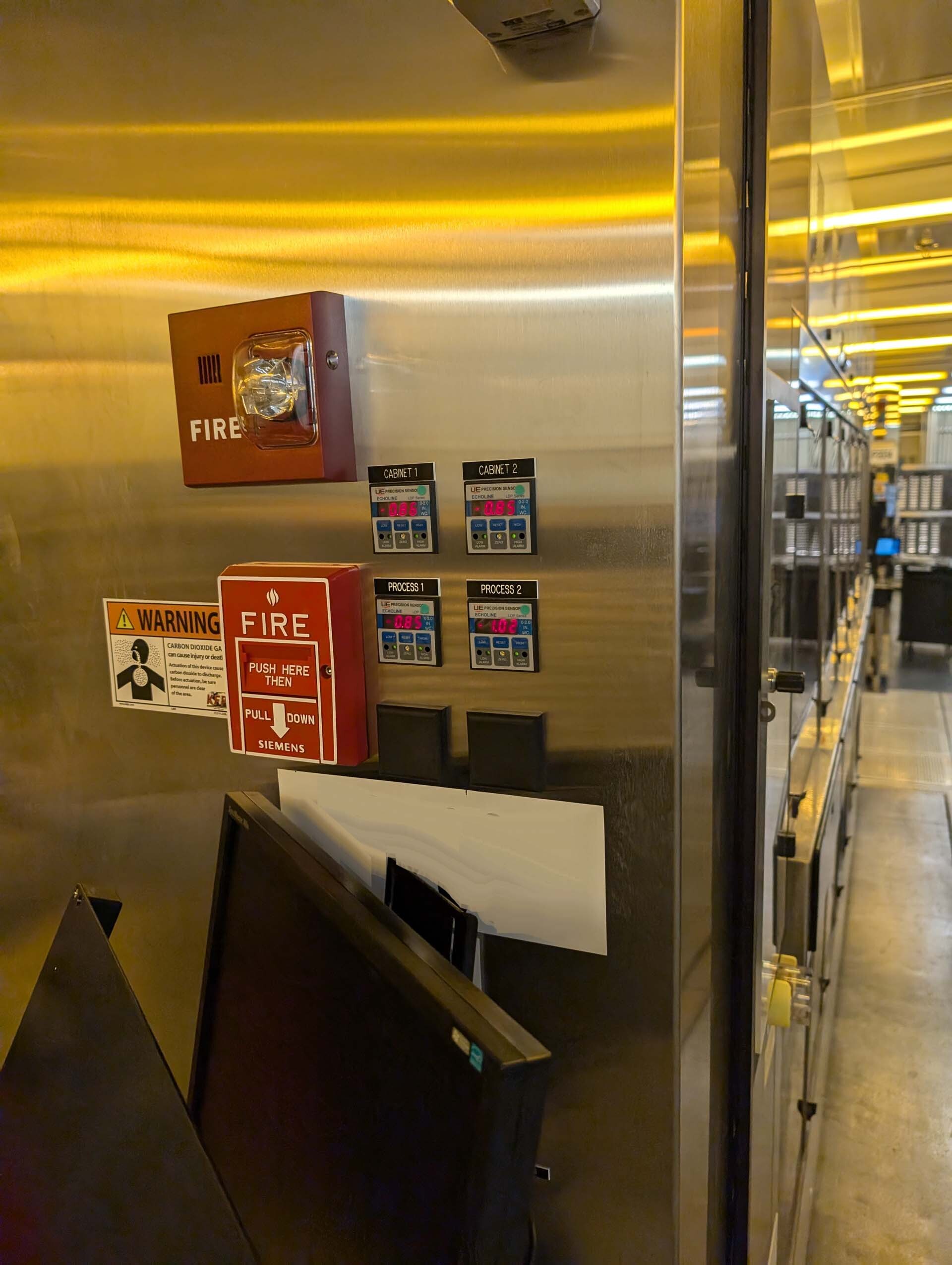
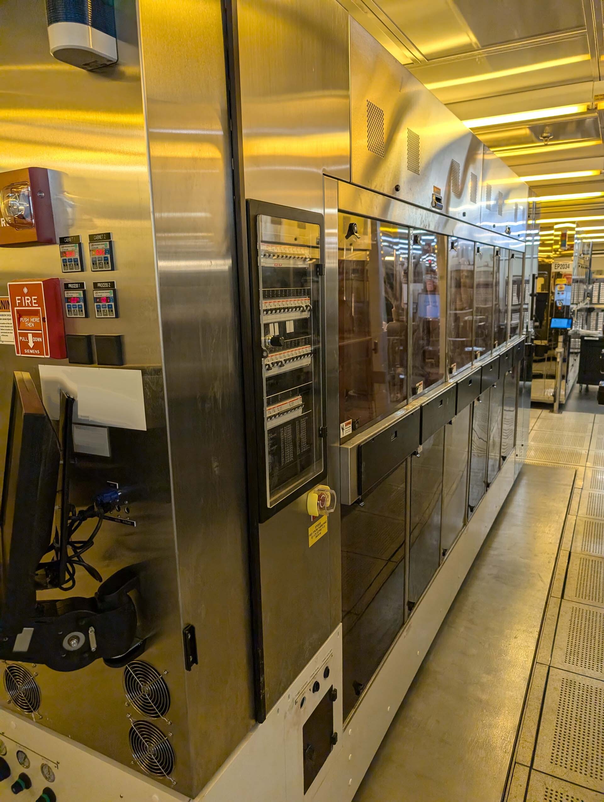
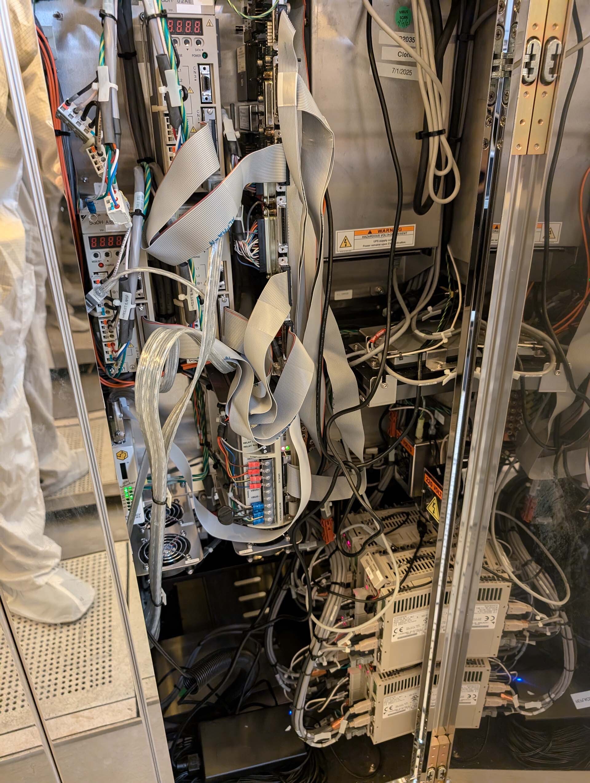
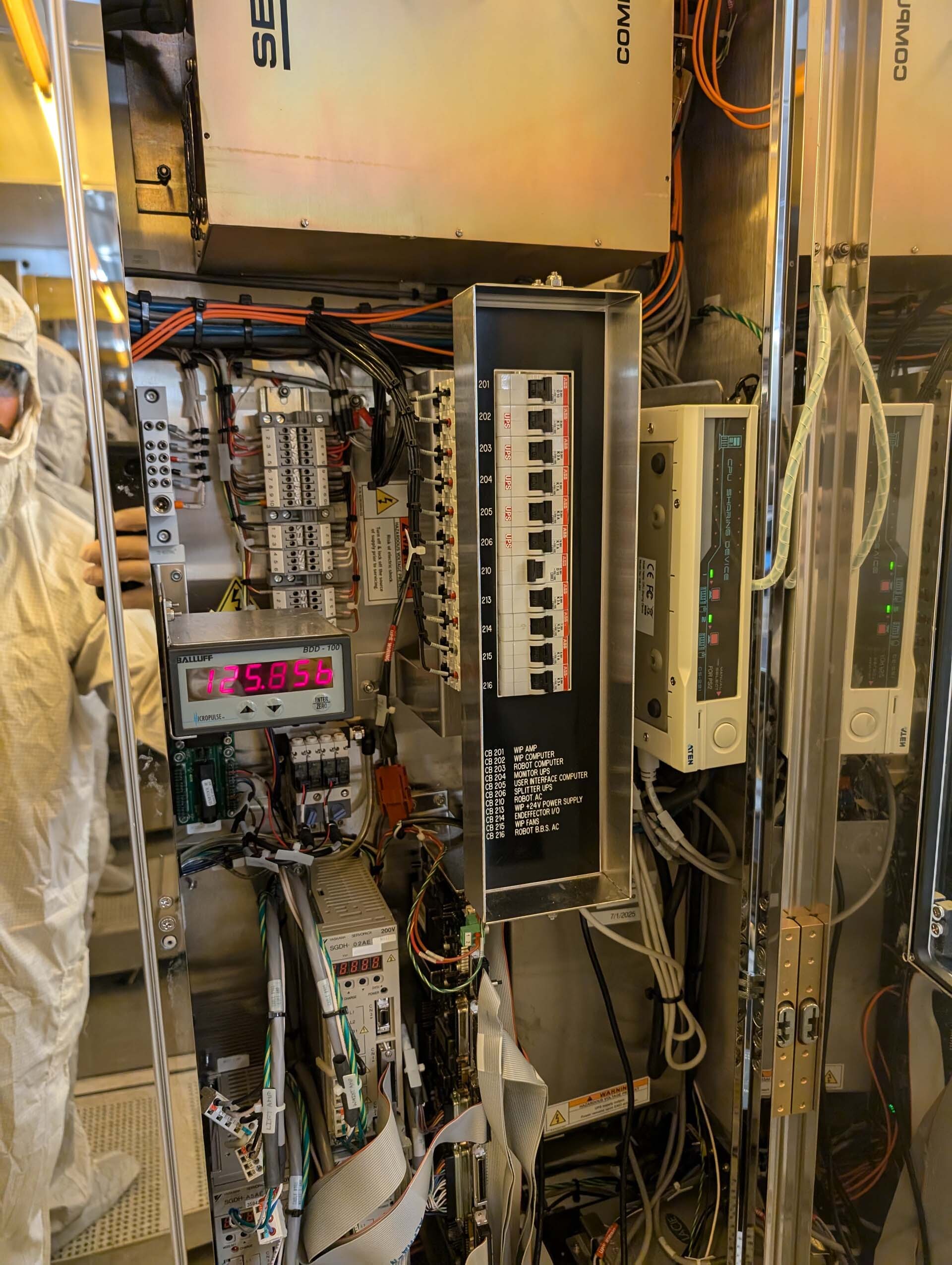
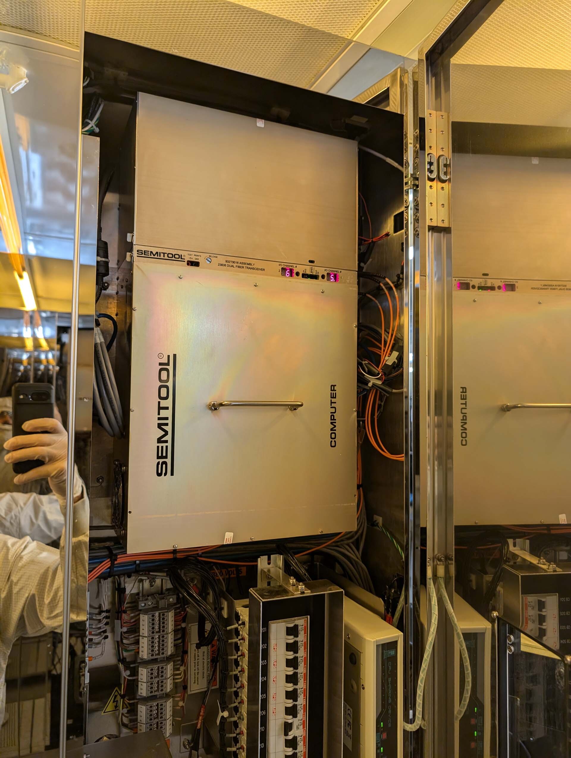
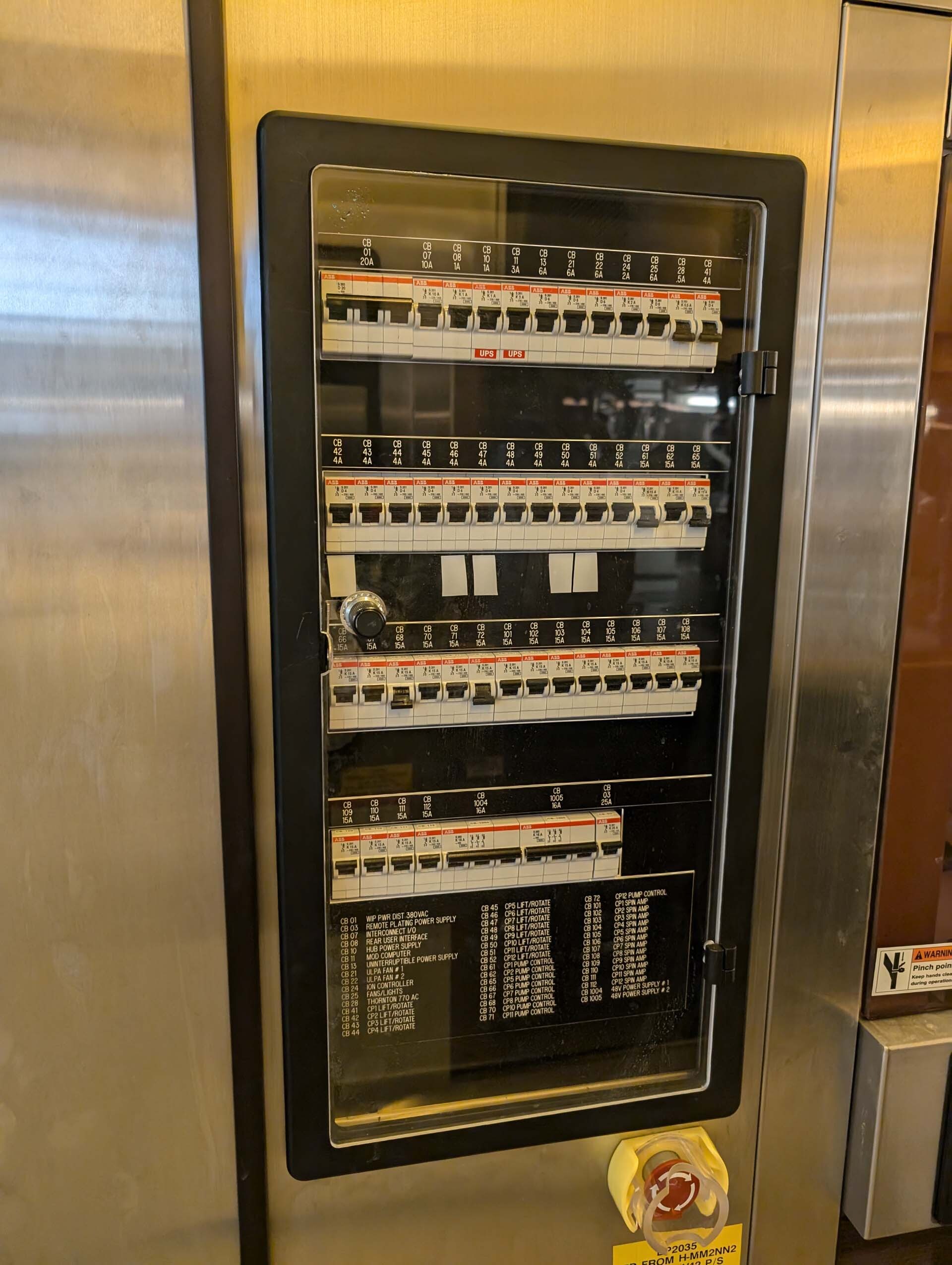
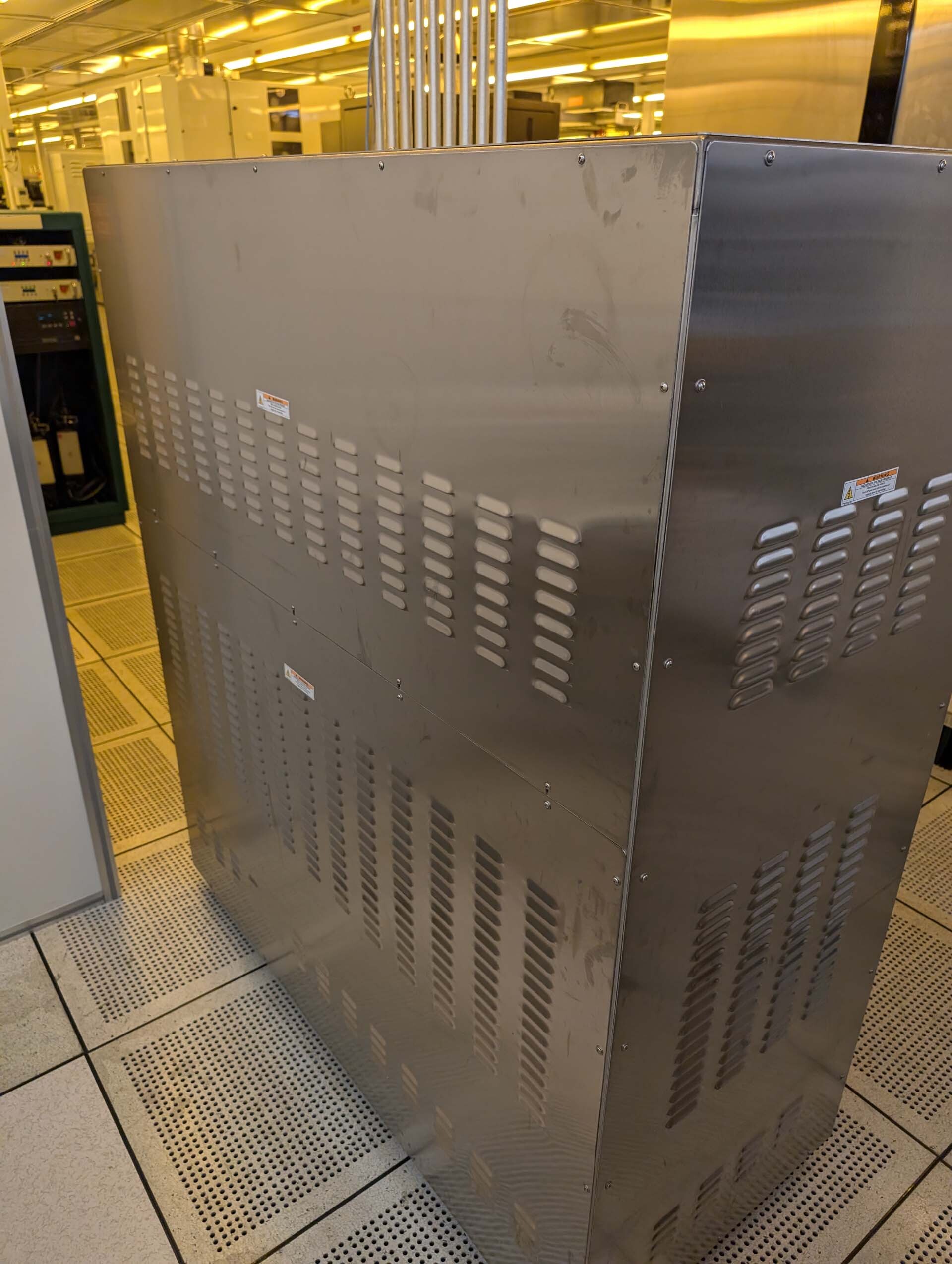
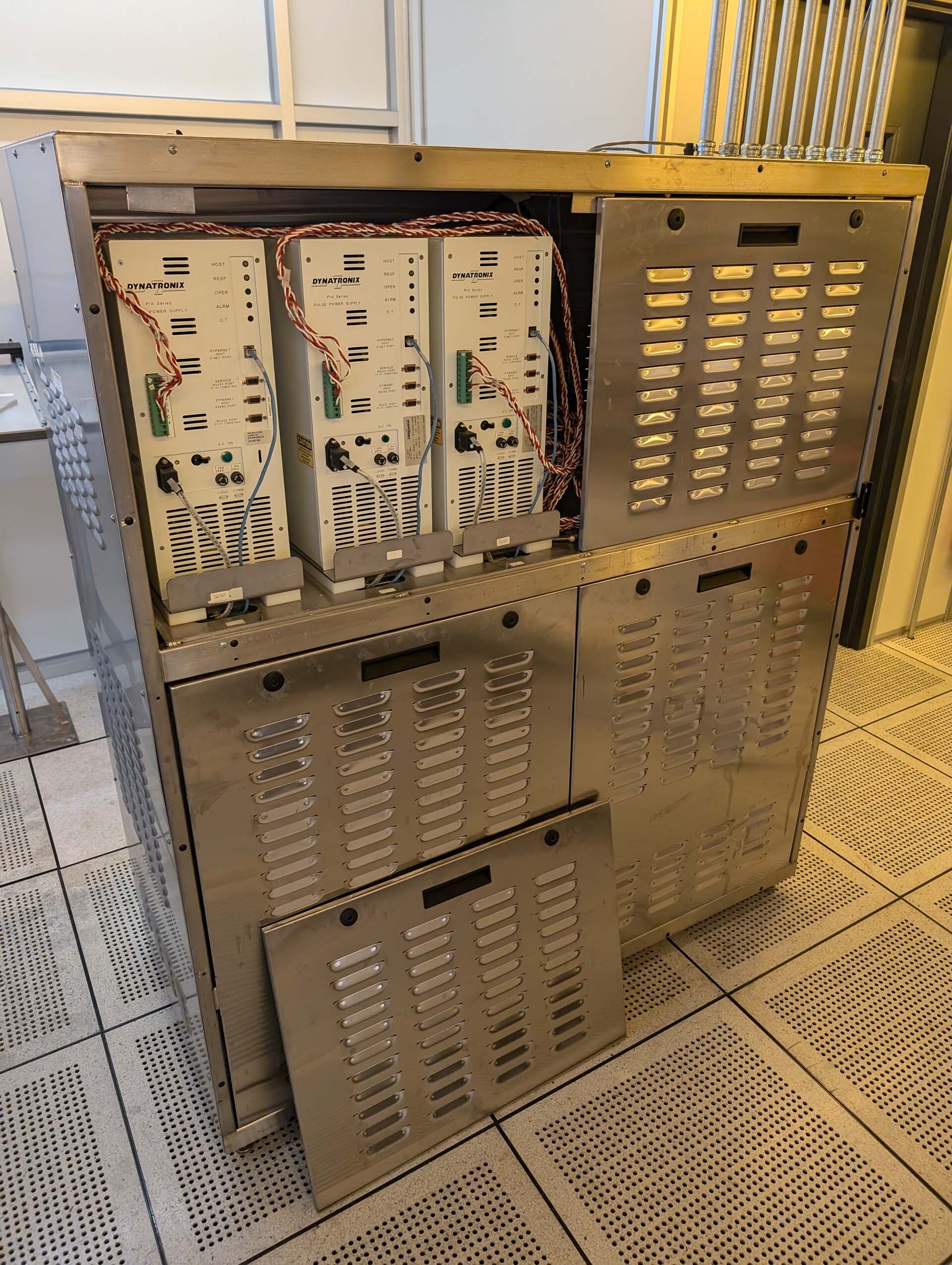
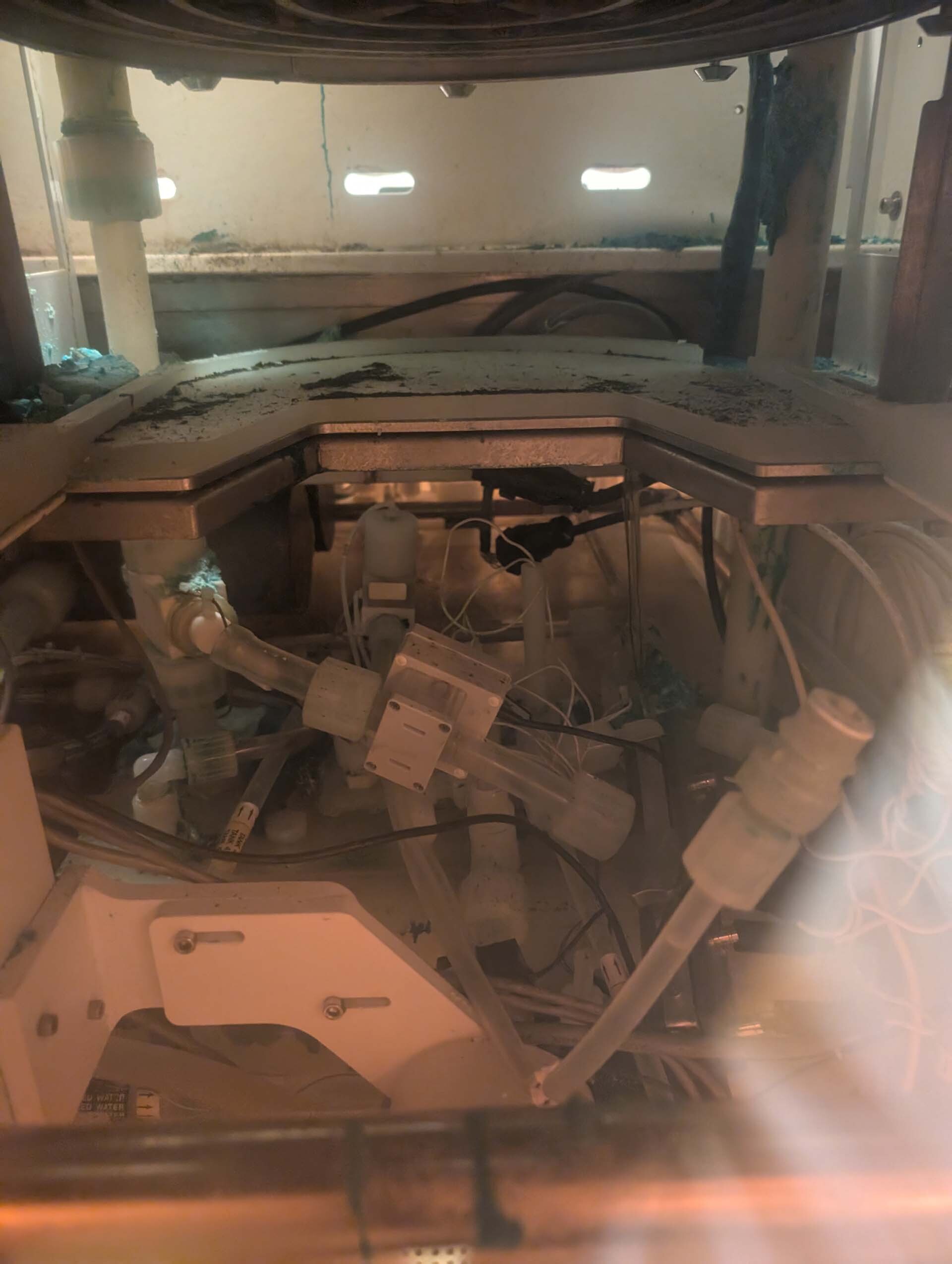
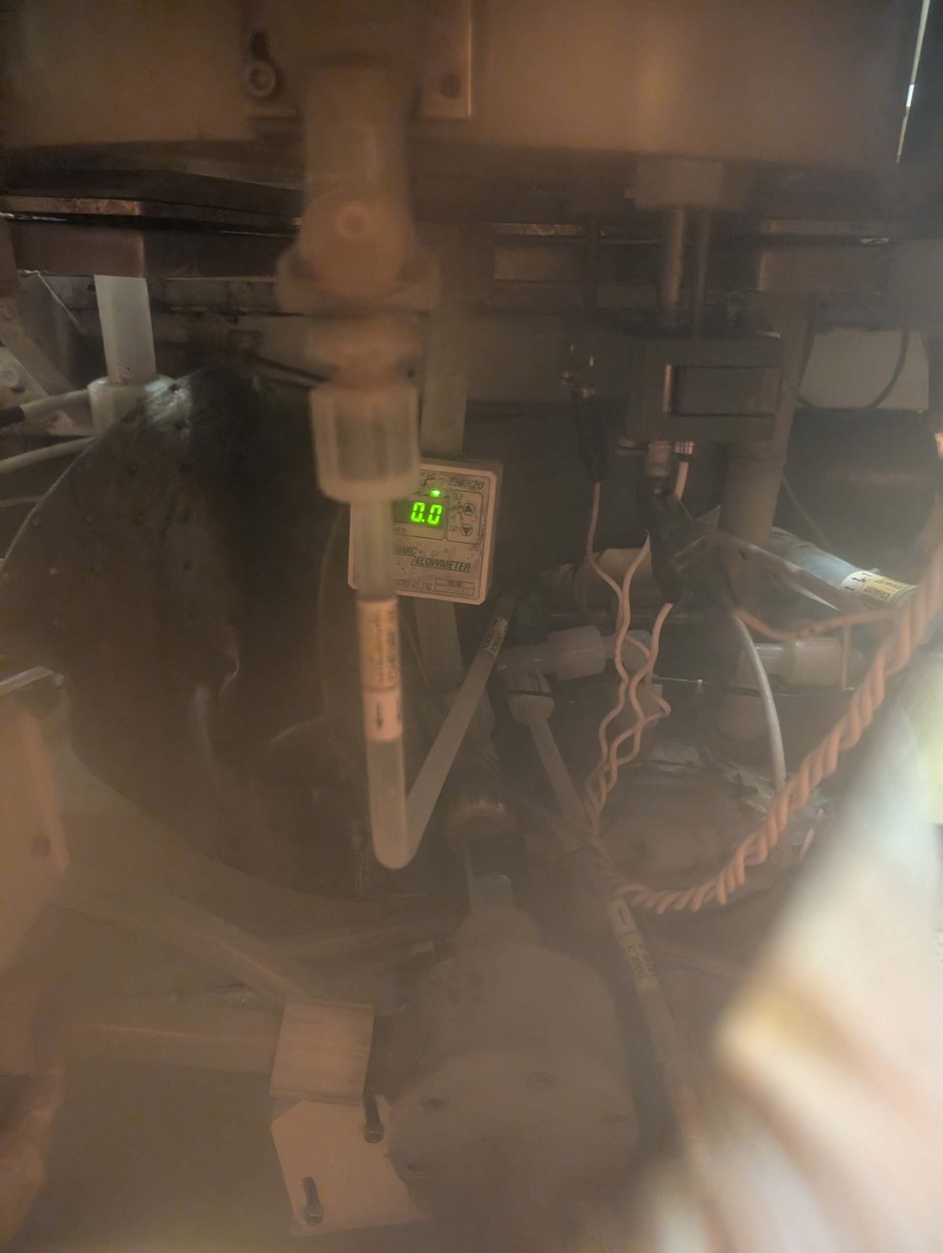
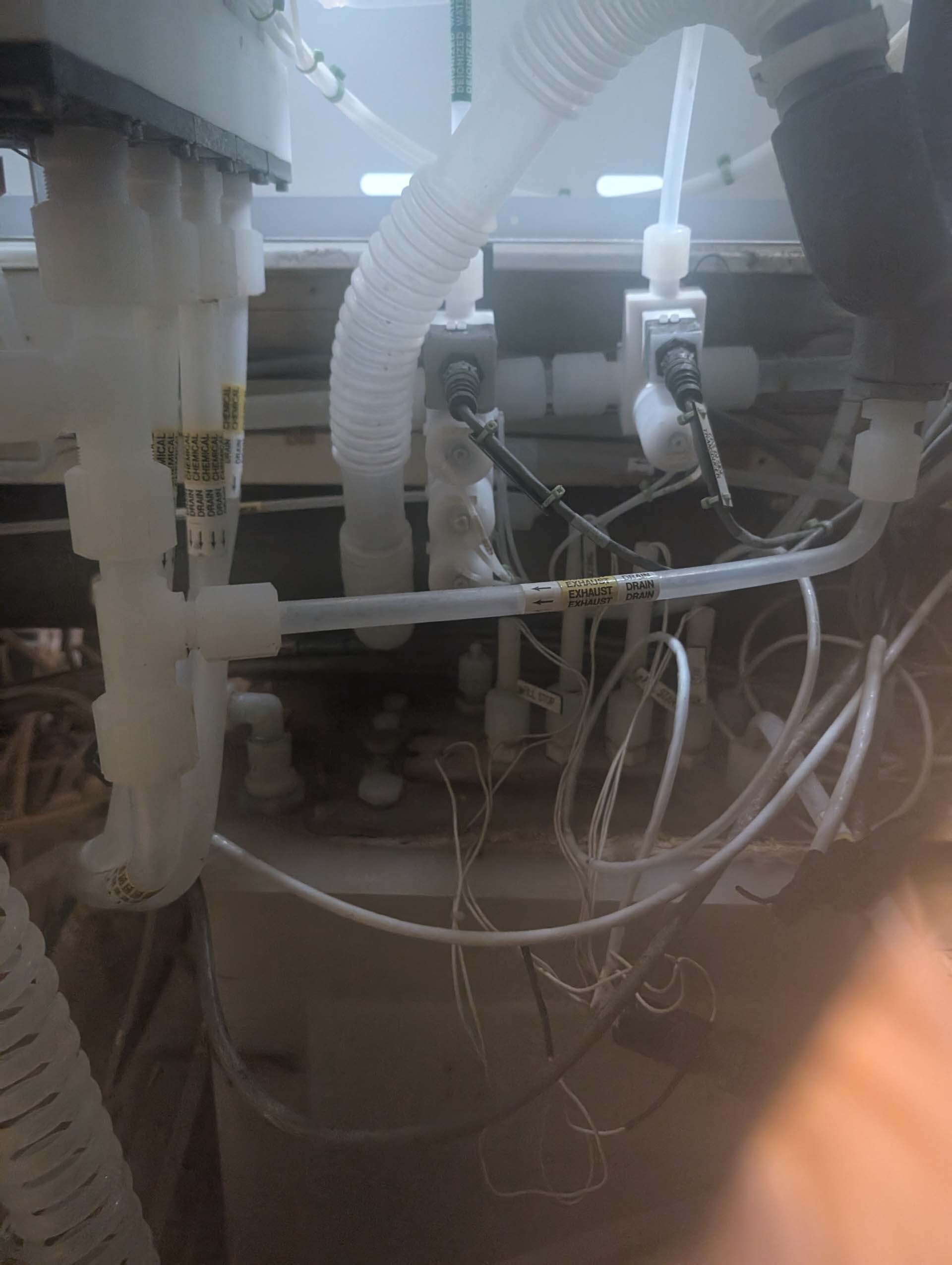
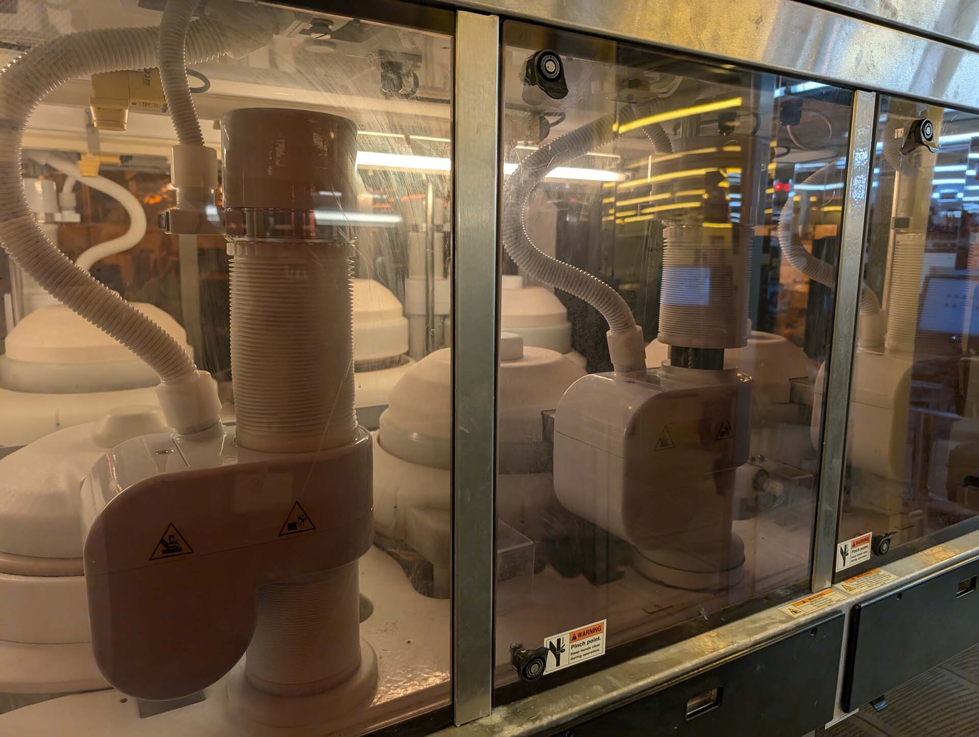
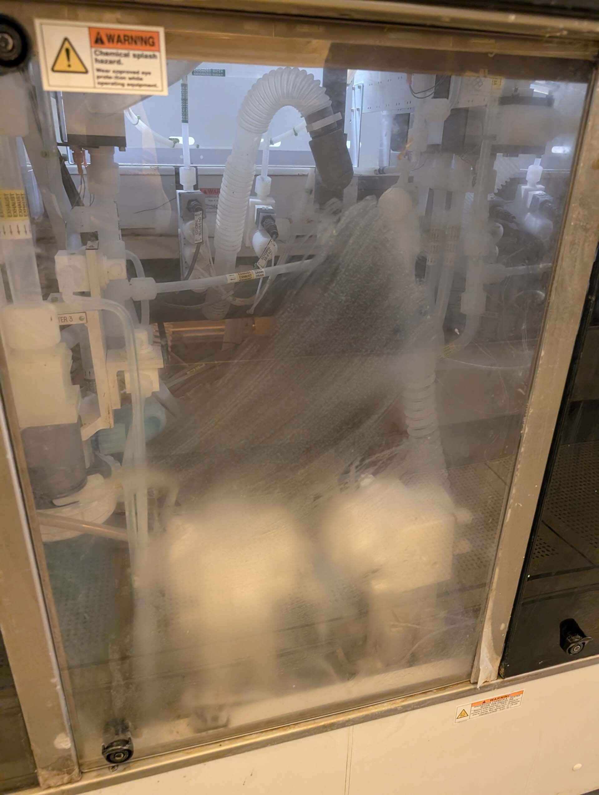
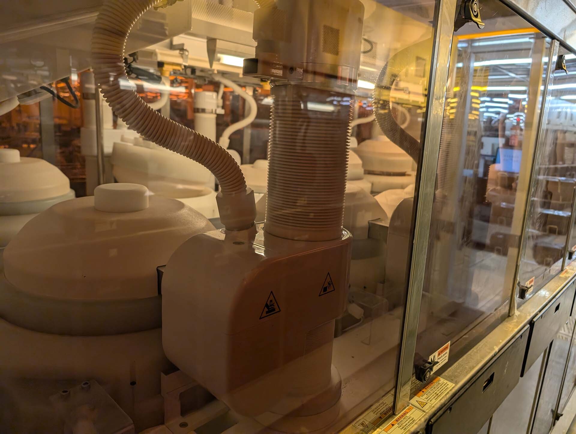
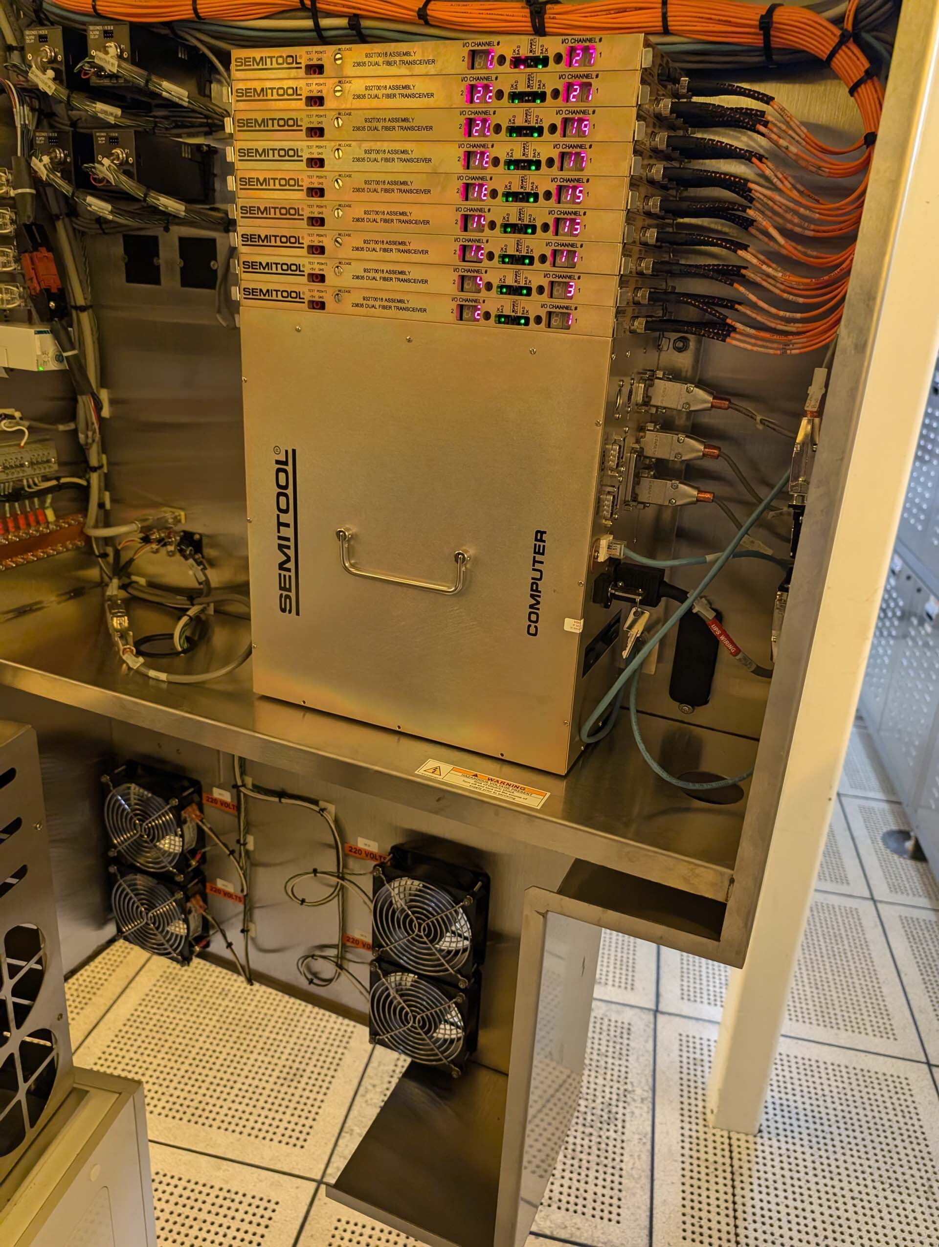
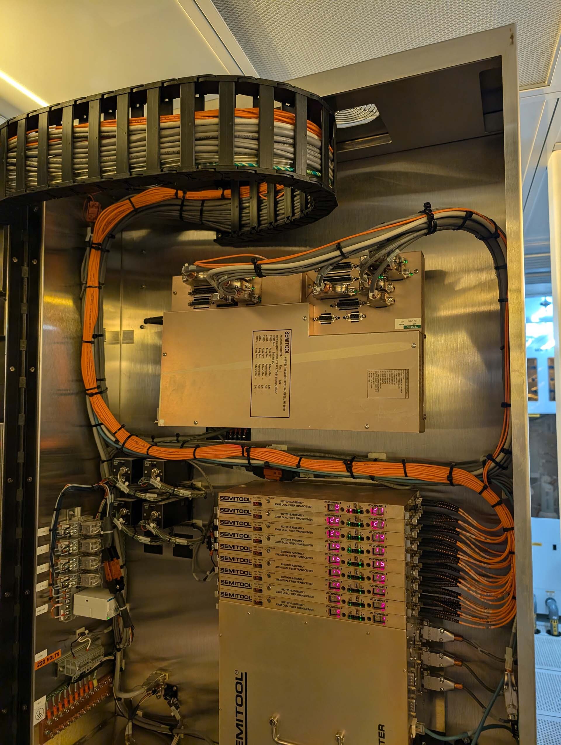
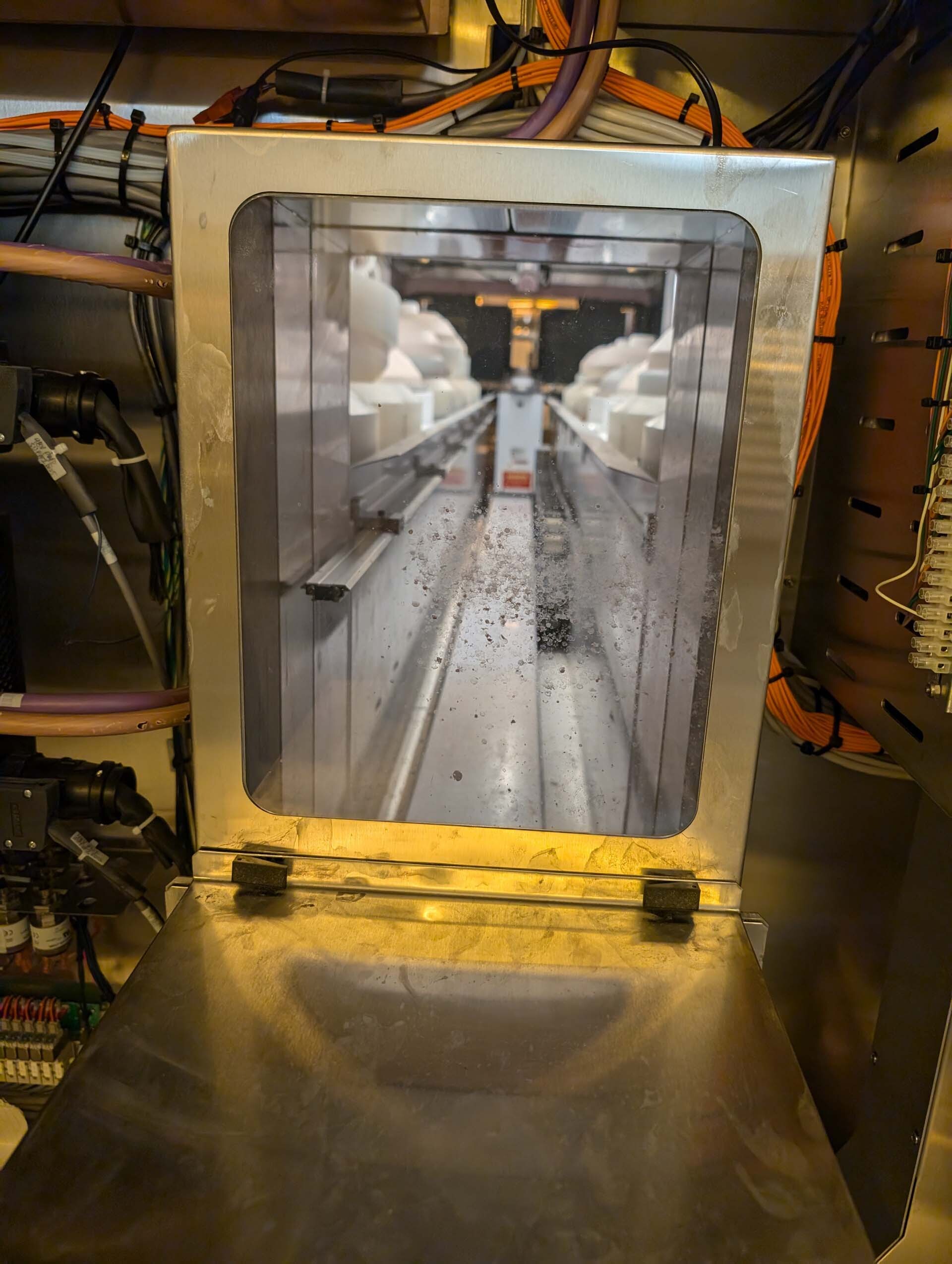
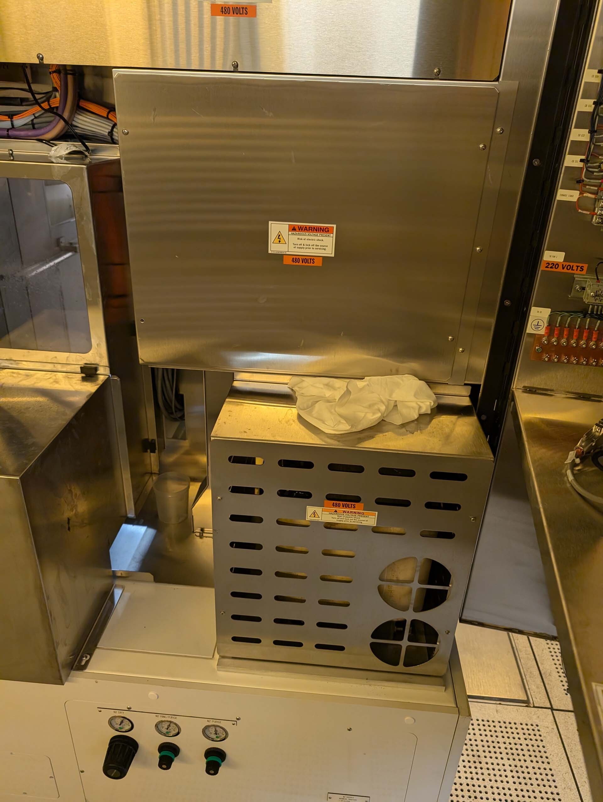
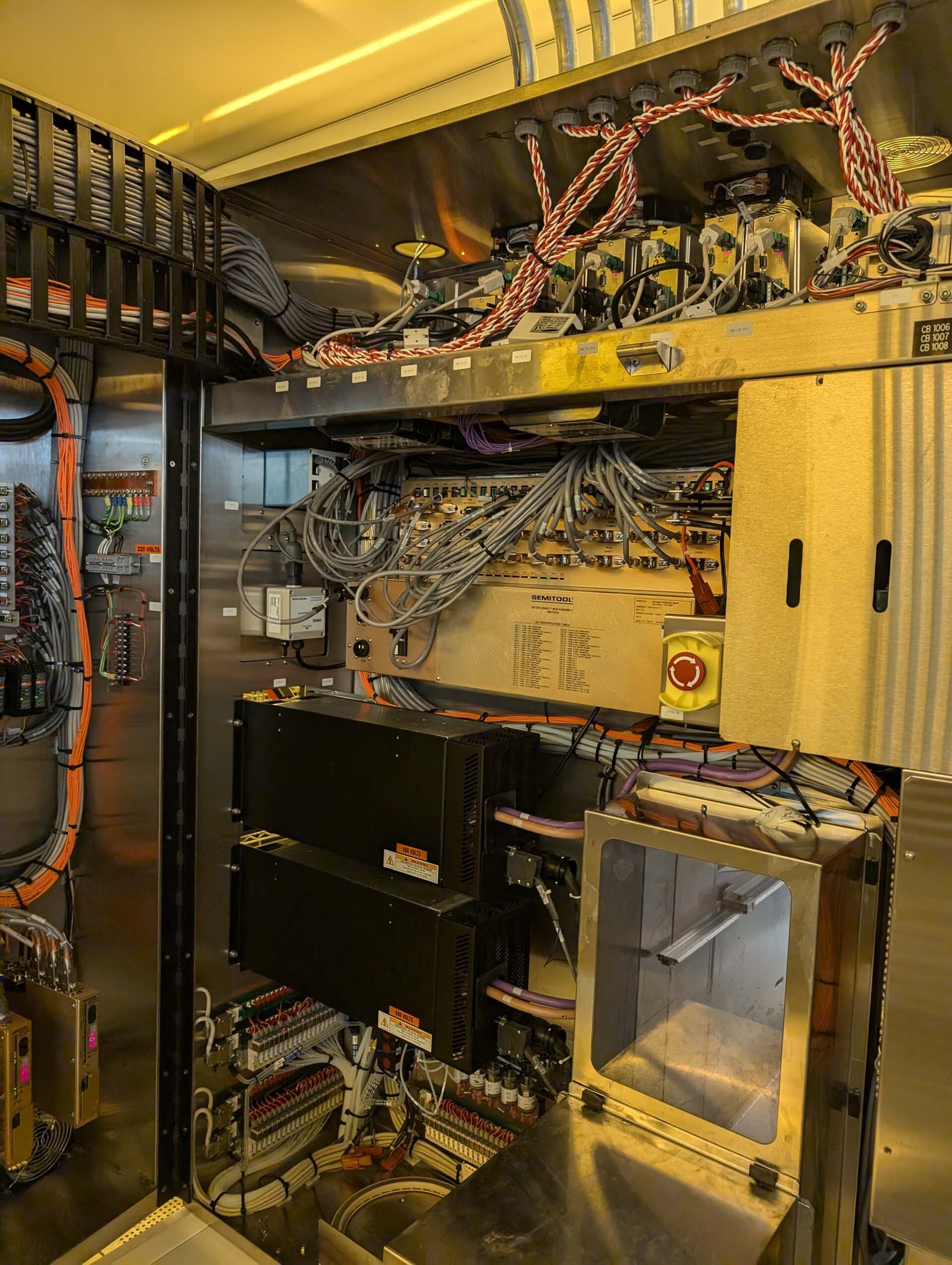
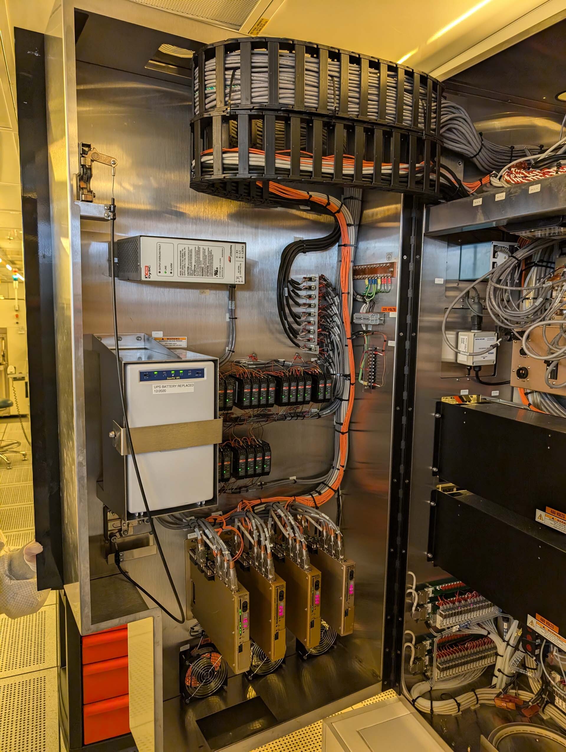
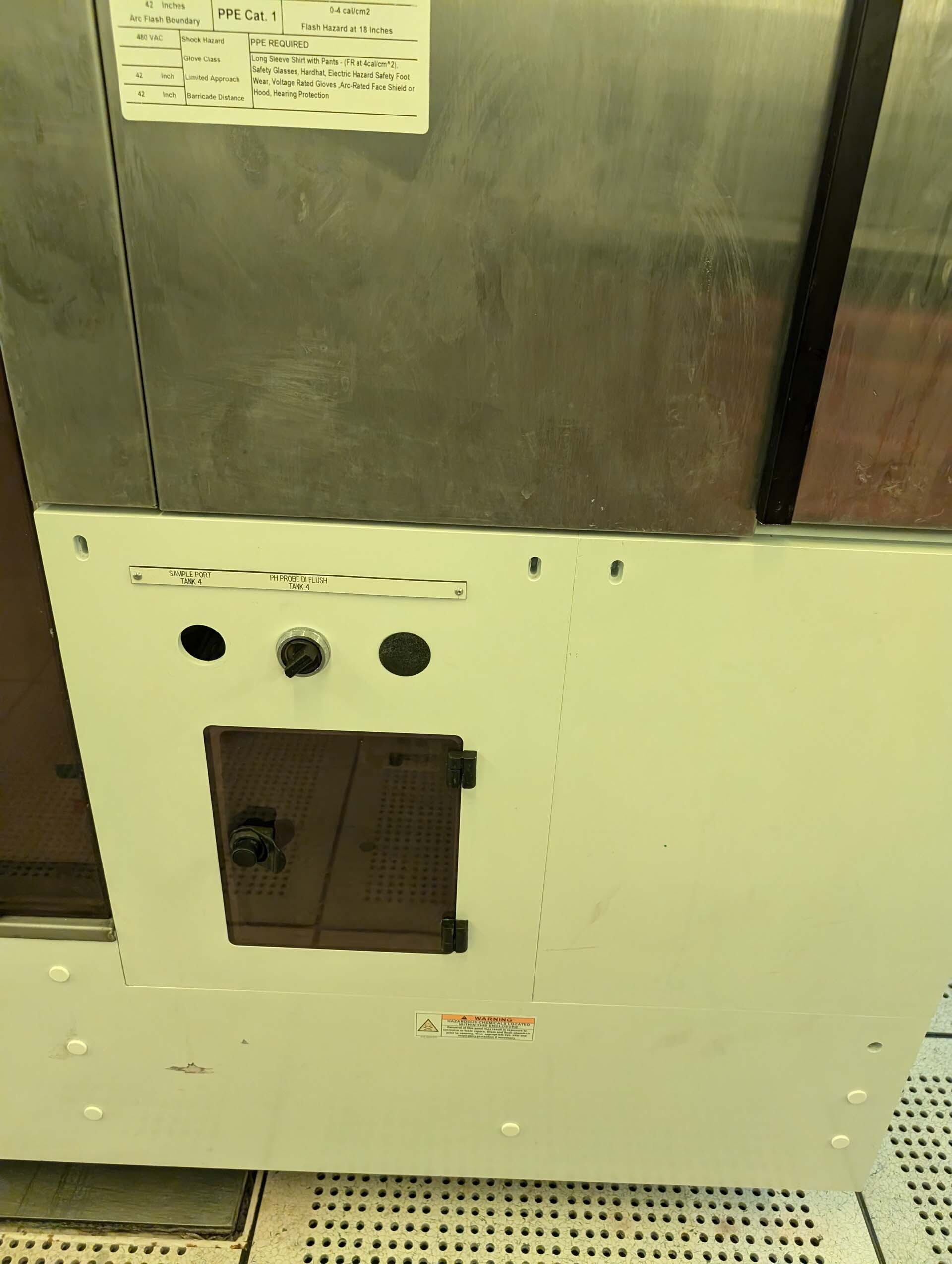
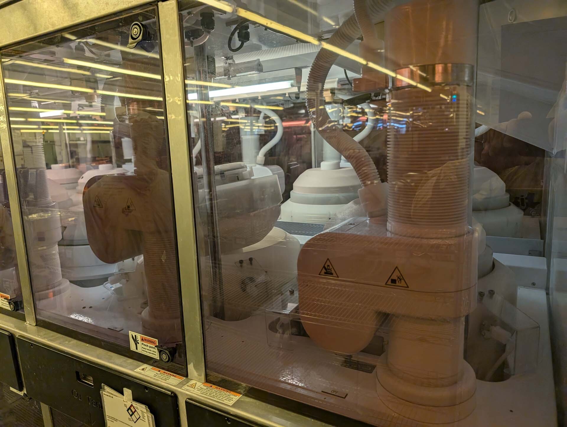
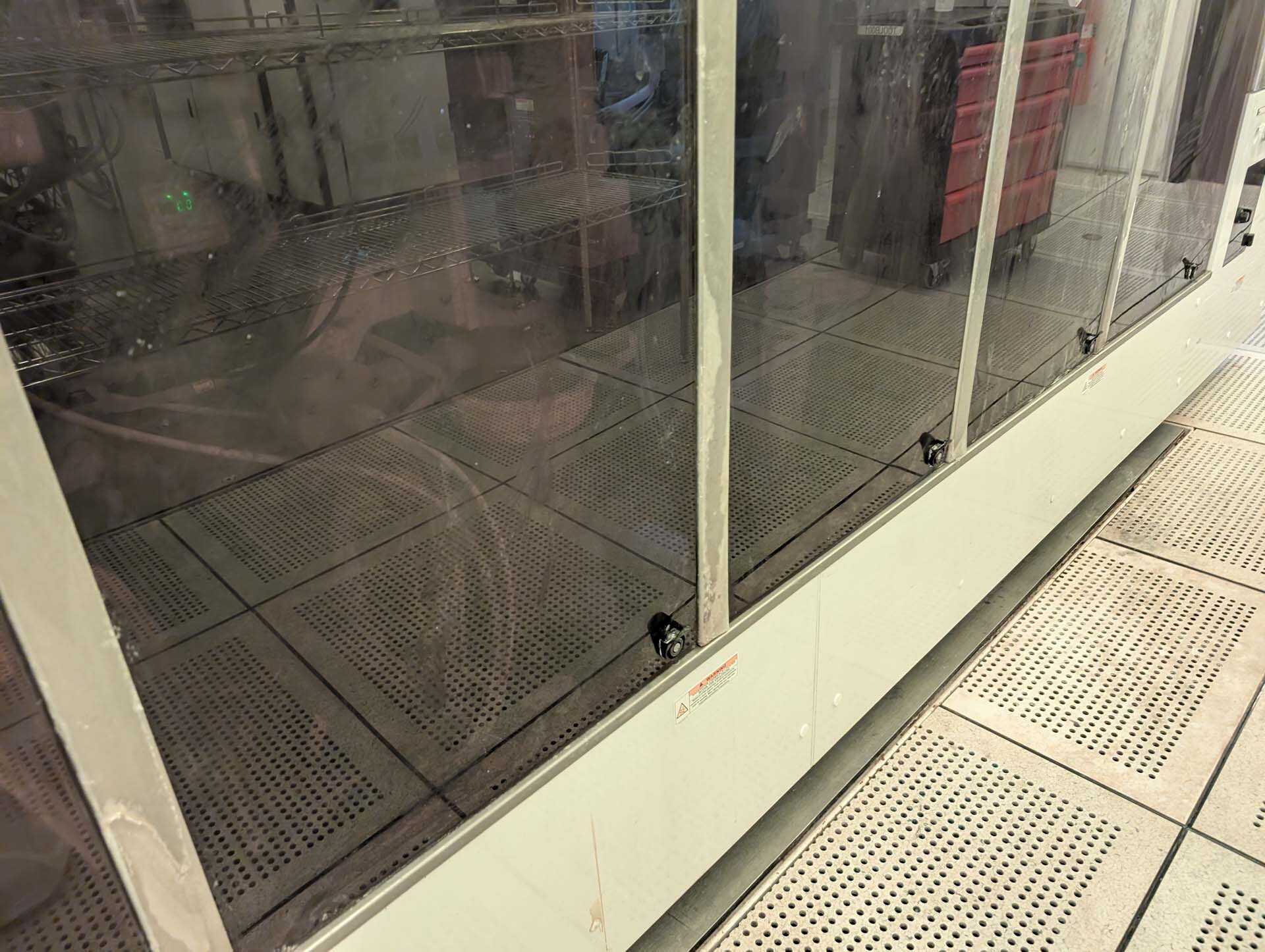
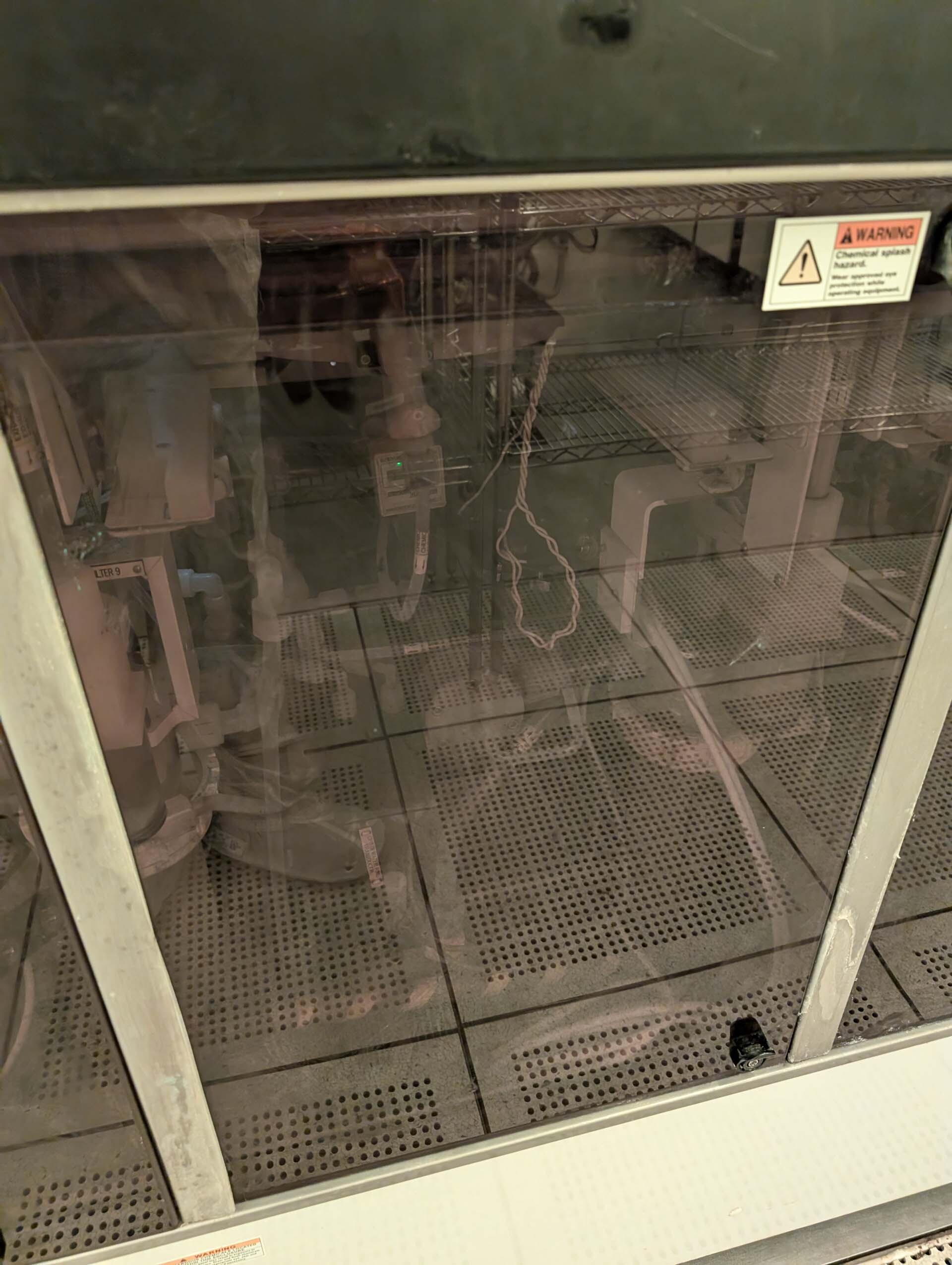
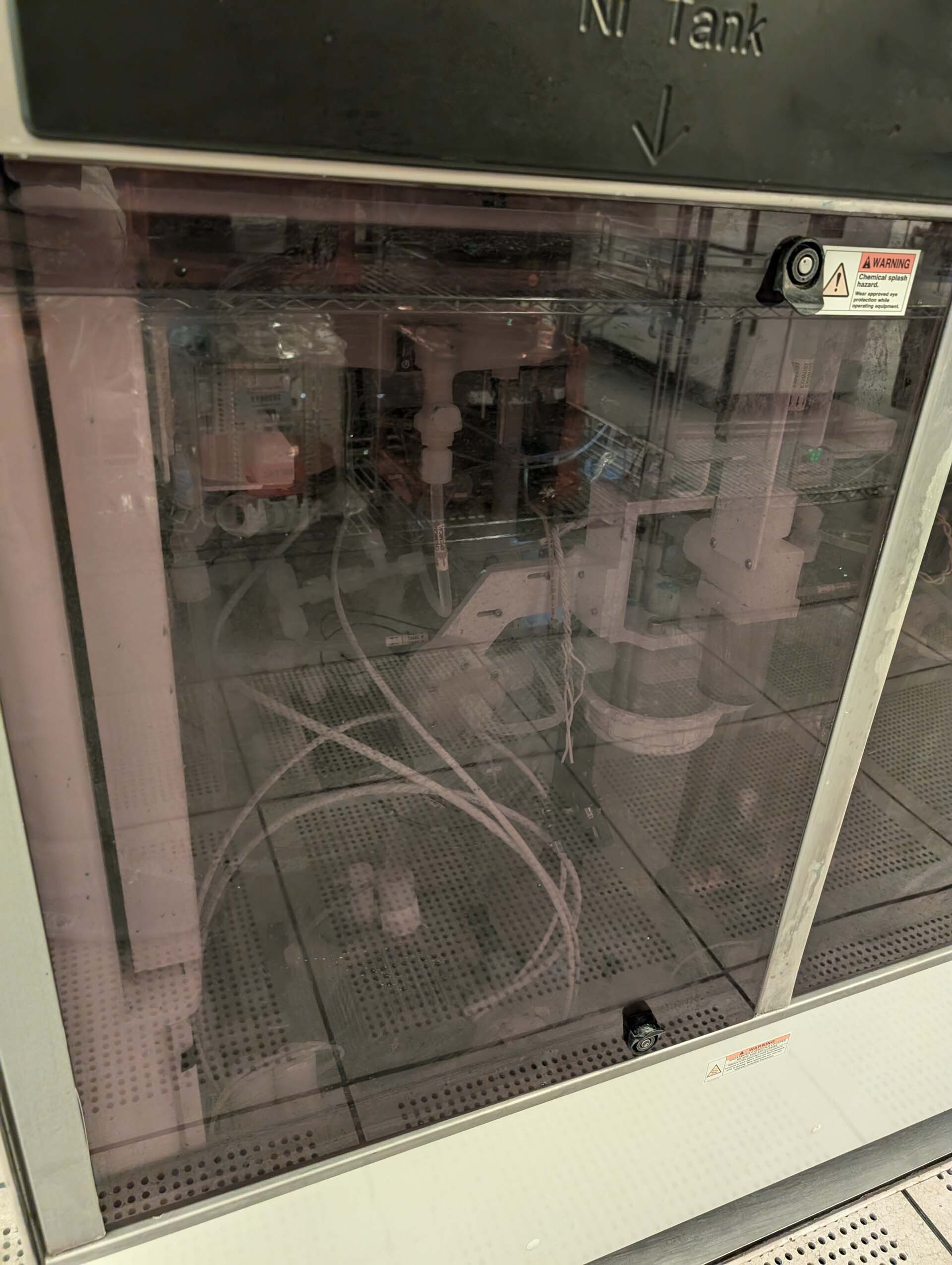
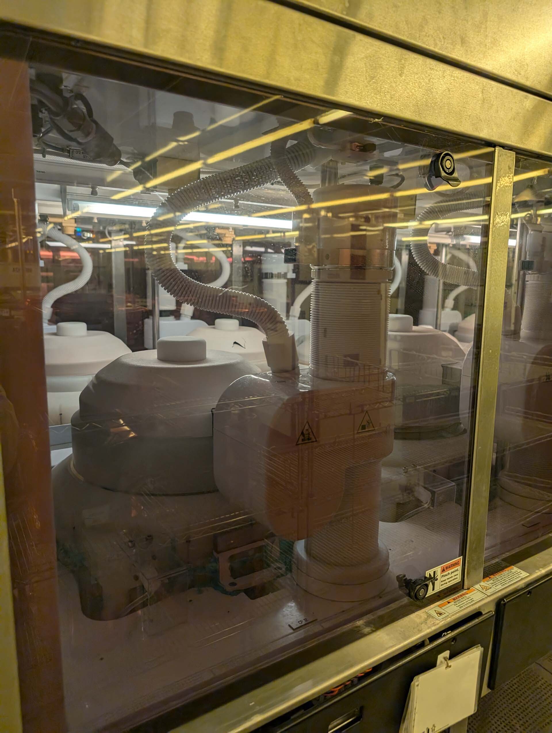
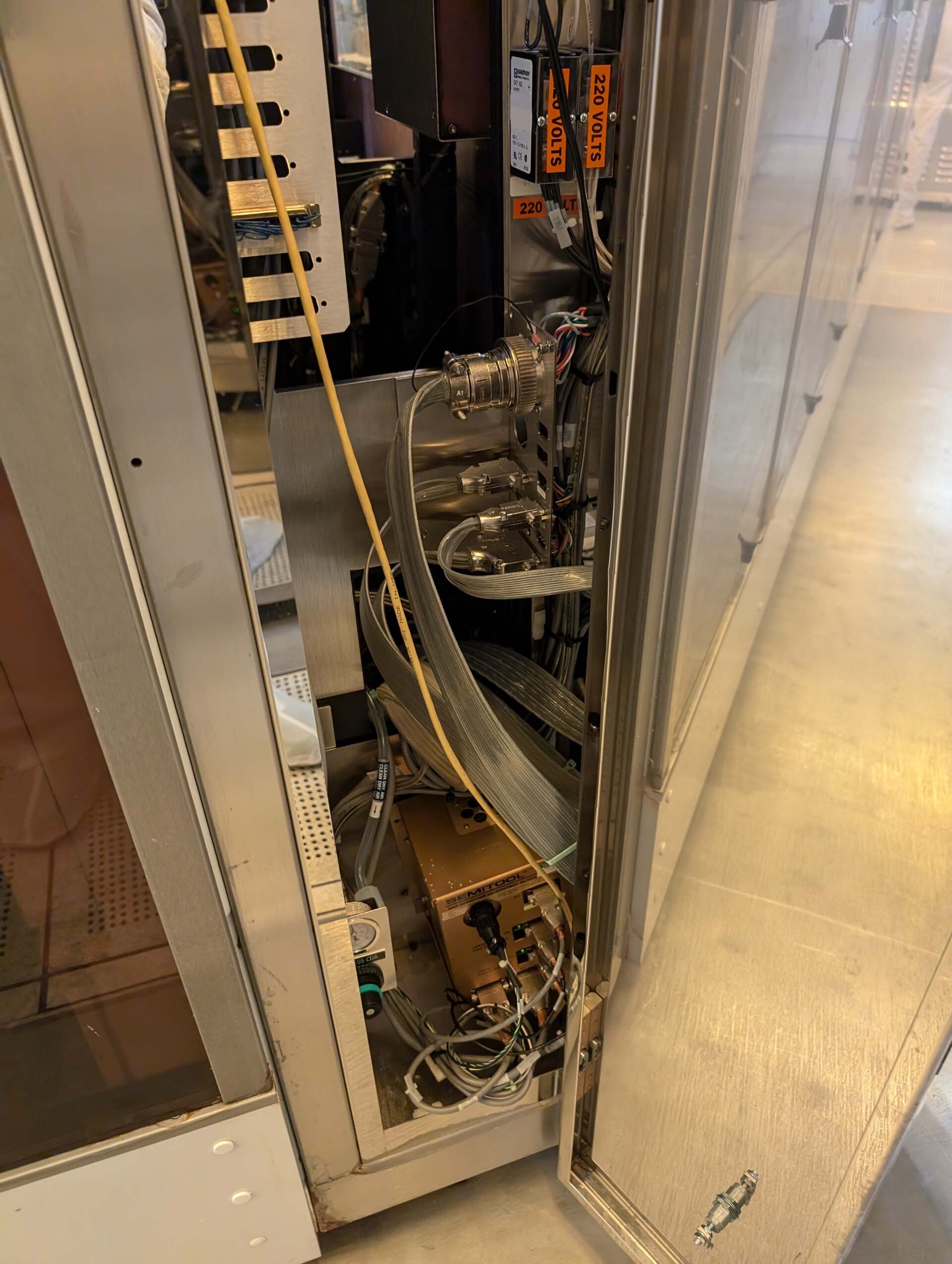
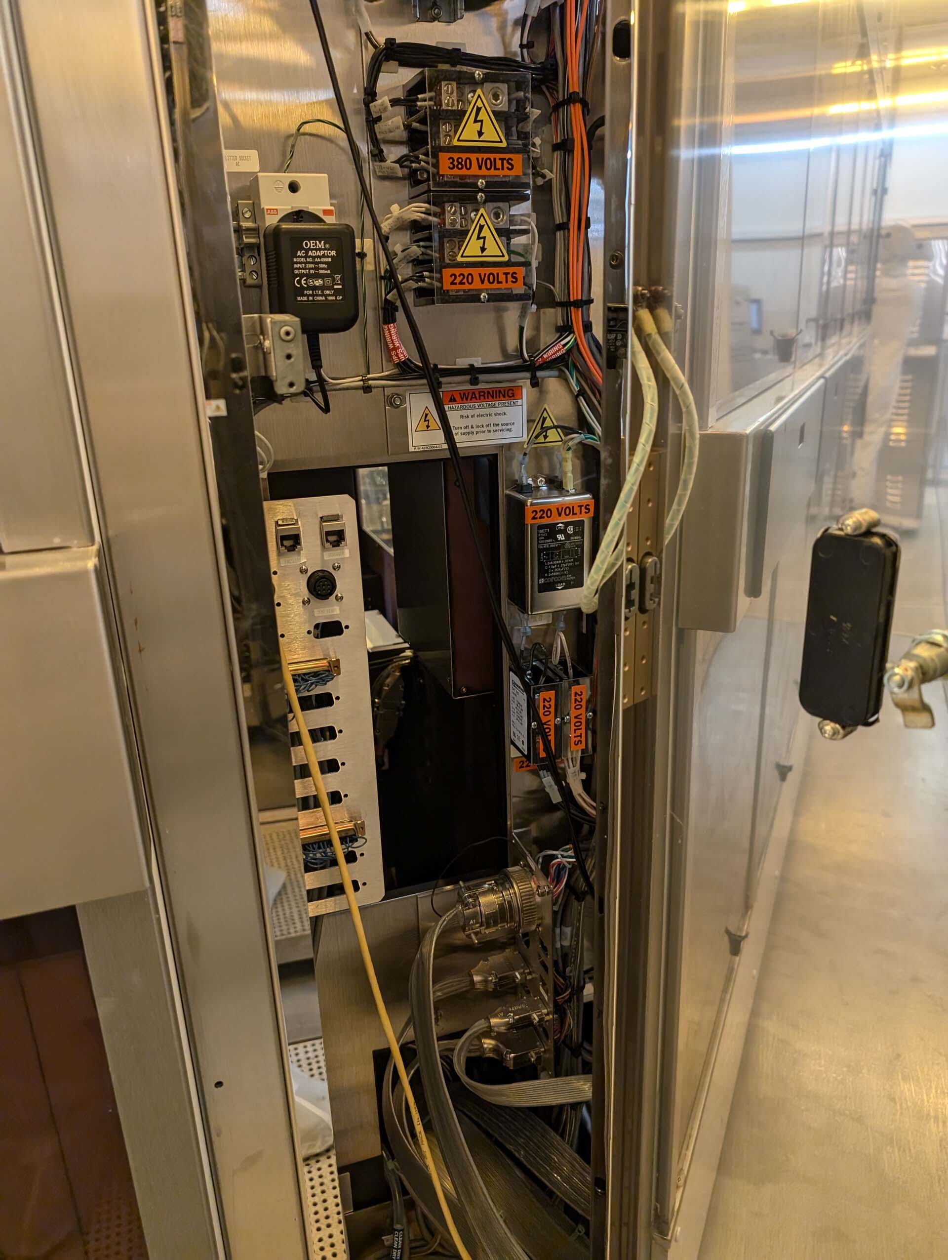
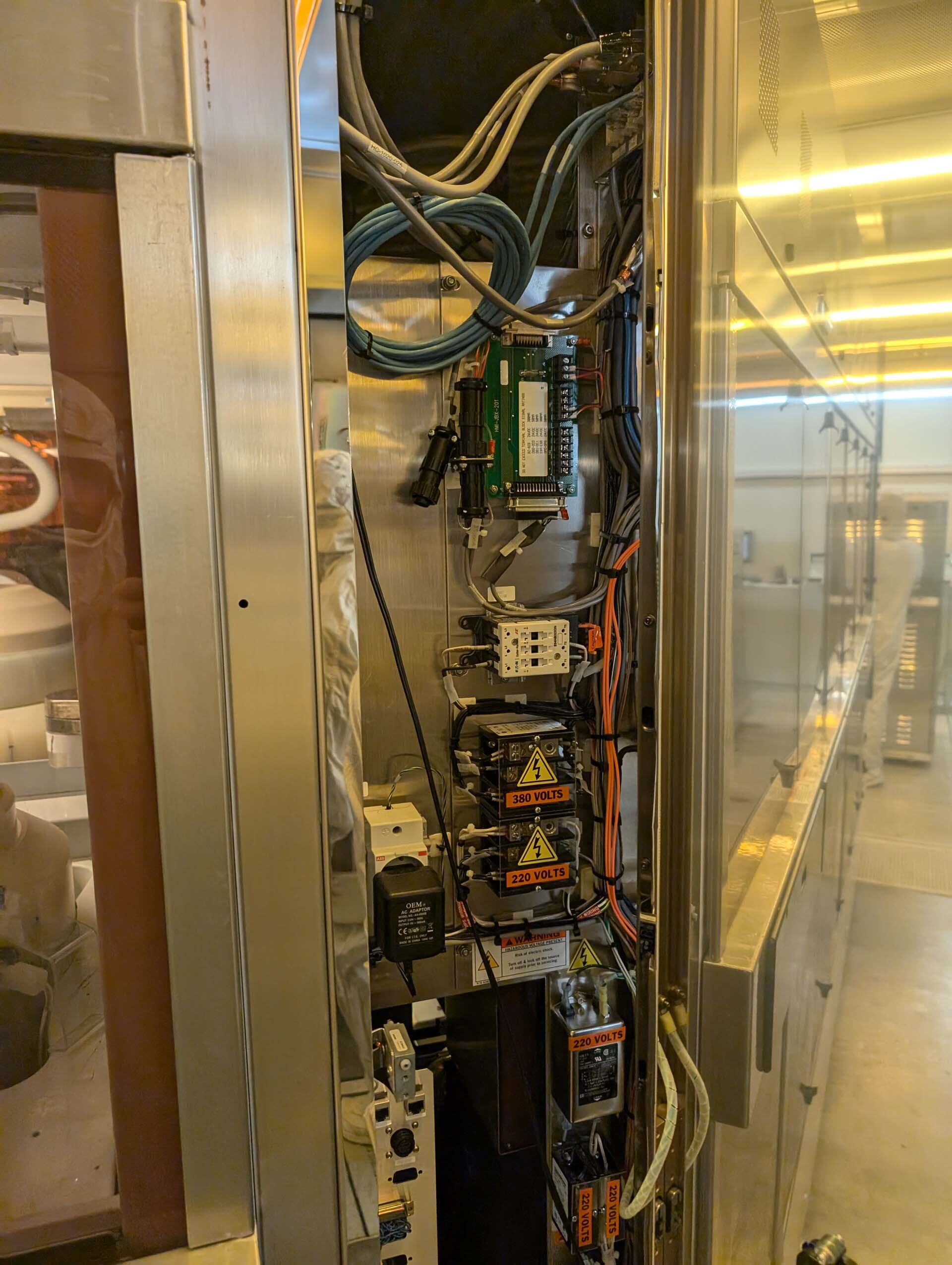
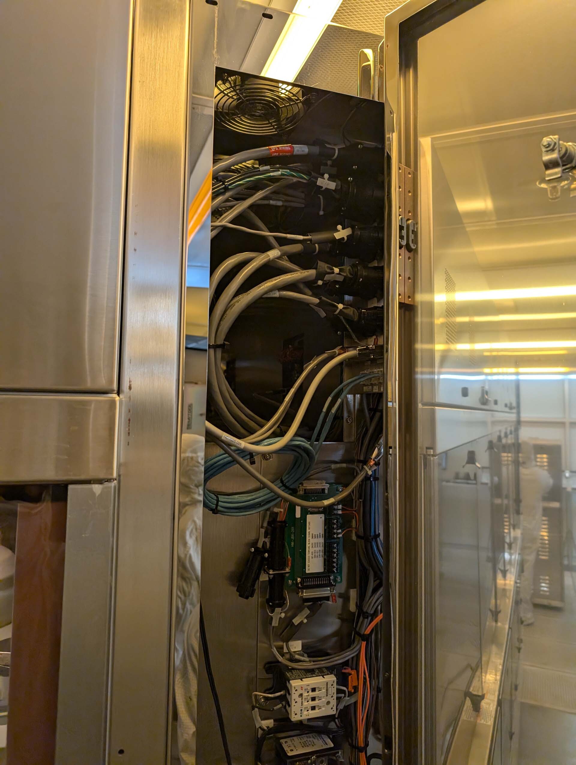
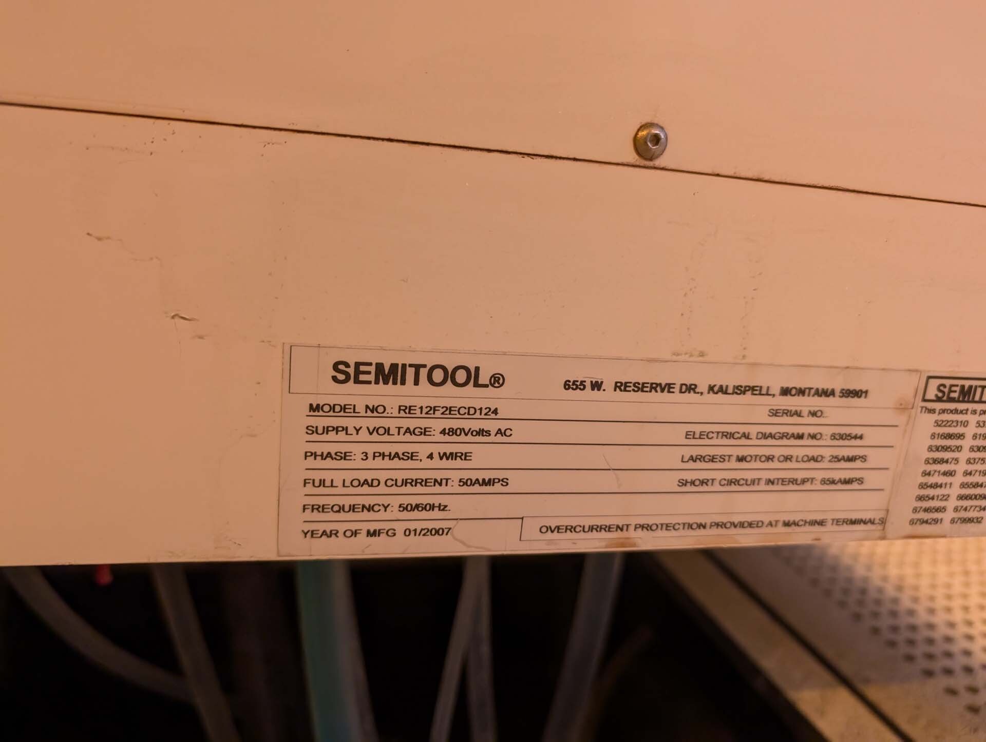
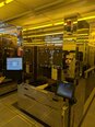
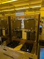
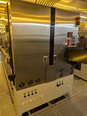
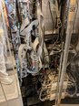
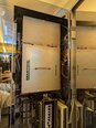
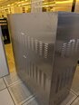
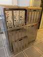
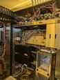
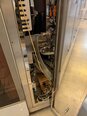
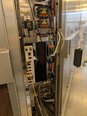
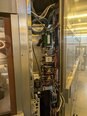
SEMITOOL Raider ECD 312 is an advanced photoresist system designed to enable high-precision photolithography processes for a range of applications. Photolithography is a key part of semiconductor processing and involves the transfer of a pattern from a mask to the surface of a substrate using light and photo-sensitive chemicals. SEMITOOL RAIDER ECD-312 provides a highly efficient, automated platform for this process. Raider ECD 312 is designed to handle a range of different materials, such as silicon, sapphire, glass and quartz. It supports a variety of wafer sizes, from 2-inch to 8-inch diameter wafers. It is also capable of handling more sensitive process steps such as ultra-violet exposure, deep-UV exposure and thermal processing. RAIDER ECD-312 has advanced control and handling capabilities, allowing for accurate and repeatable patterns to be produced. It is capable of imaging at up to 8 micron resolution and controlled through a Graphical User Interface (GUI). It has an integrated microprocessor which is used for process monitoring and calibration. It is equipped with a multi-zone heating plate, enabling precise temperature control in each zone, as well as a technique called multi-focusing which maintains a high-precision focus in the presence of irregular wafer shapes. SEMITOOL Raider ECD 312 also includes a conveyor system which is used to move the wafers through each step of the photolithography process. It includes multiple camera systems which are used to monitor the wafer at different stages of the process. An automated cleaning nozzle is also included for cleaning the photoresist from the wafers. SEMITOOL RAIDER ECD-312 is one of the most advanced and reliable photolithography systems available and is ideal for producing complex patterns for photovoltaic devices, flat panel displays and other high-resolution applications. Its combination of efficient, automated handling and precise imaging capabilities makes it a great choice for a wide variety of semiconductor fabrication processes.
There are no reviews yet