Used SEMITOOL WST-308A1CCBT #293660328 for sale
URL successfully copied!
Tap to zoom
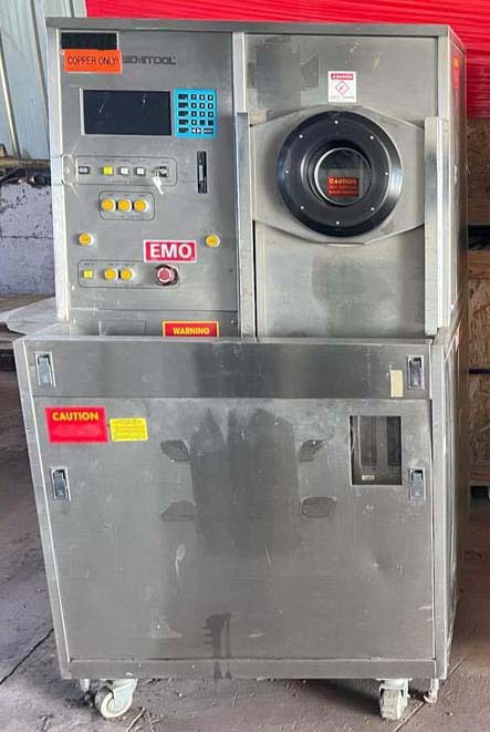


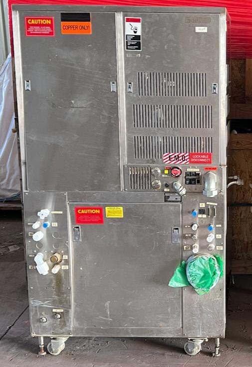

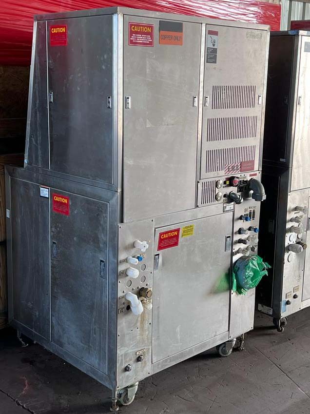



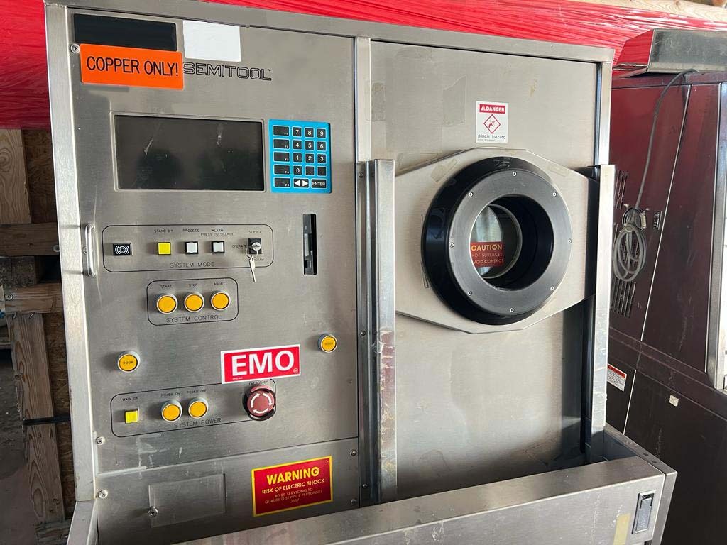


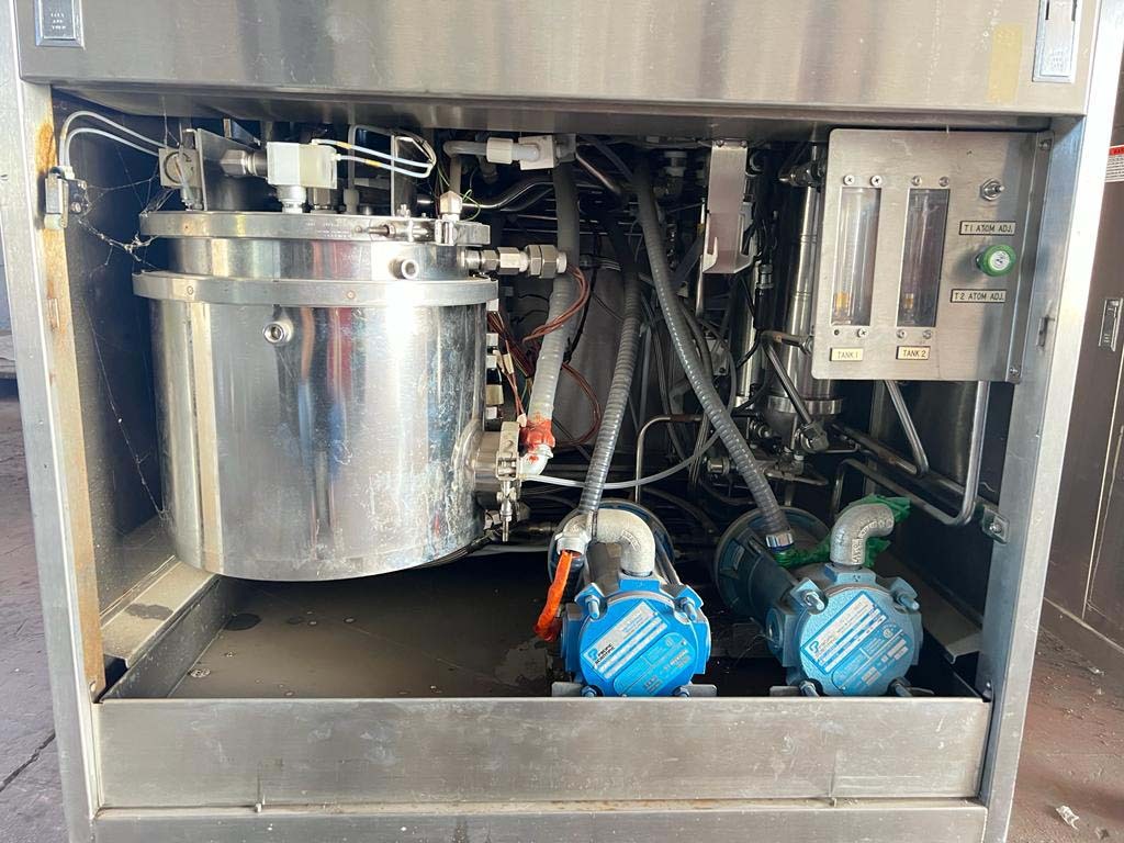


SEMITOOL WST-308A1CCBT is a photoresist equipment designed for advanced semiconductor lithography applications. This system has been developed to enable faster, more accurate, and higher yields of sensitive photoresist processes that are used in the fabrication of semiconductor devices. This unit features a single-wafer loadlock, a turbo molecular pump, a digital temperature controller, and a fully interlocked safety machine. It features an advanced optical alignment tool to ensure precise, repeatable positioning of wafers for lithography processes. Additionally, SEMITOOL WST-308A-1CC-BT features a programmable logic controller (PLC) that enables users to configure individual recipes and manage asset log data. To ensure a steady and safe environment, the model also achieves a maximum base pressure of < 2.5 x 10⁻⁶ Torr. When used for photoresist processing, WST-308A1CCBT equipment offers a 45° tilted angle platform that helps to reduce the static and dynamic forces to achieve higher throughputs. The integrated wafer boat system can accommodate up to 8 wafers with a single-wafer loadlock. The unit features an advanced wafer temperature control machine that ensures uniform wafer temperatures of +/- 0.5°C, which is critical for consistent photoresist exposure. The tool also features adjustable dipole and bipolar chambers for variable photoresist level and uniformity. Additionally, rapid subsystem achieve speeds up to 1,800°C/min ensure that every litho cycle produces superior results. WST-308A-1CC-BT also allows for the use of both soft and hard bake processes, ensuring that the results of high aspect ratio lithography experiments remain reliable regardless of the substrate type. Finally, the large LCD display screen on SEMITOOL WST-308A1CCBT allows technicians to easily view asset information and monitor process parameters. Overall, SEMITOOL WST-308A-1CC-BT is an advanced photoresist model designed to support faster, more accurate, and higher yields of sensitive photoresist processes. Its high throughput and tightly controlled lithography parameters make it an ideal solution for advanced semiconductor device fabrication.
There are no reviews yet


