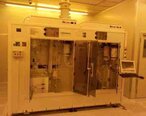
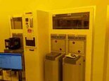
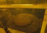
Used SEZ / LAM RESEARCH 4300 #293598011 for sale
URL successfully copied!
Tap to zoom
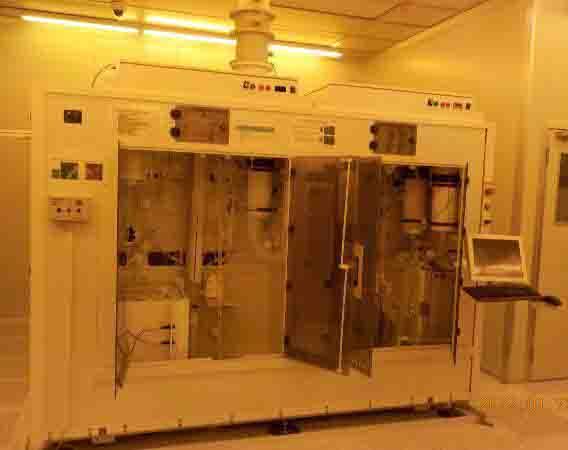

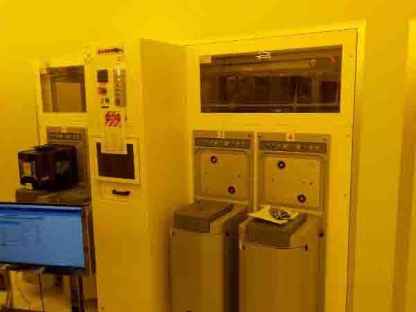

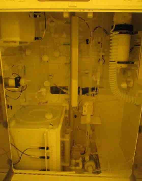

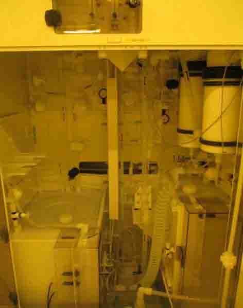


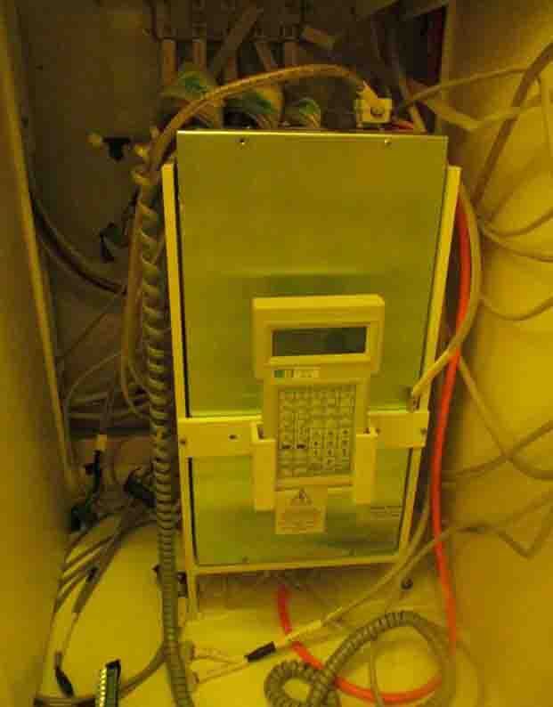






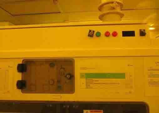


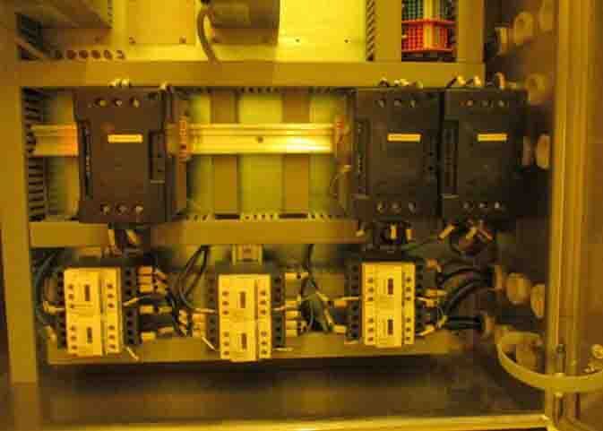

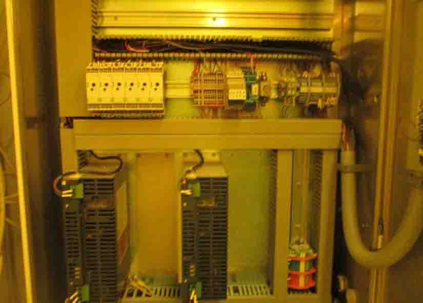


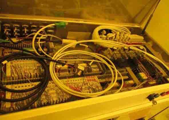









ID: 293598011
Wafer Size: 12"
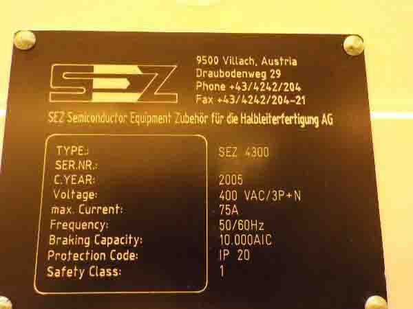
Vintage: 2005
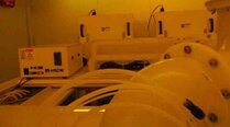
Spin etcher, 12"
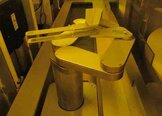
Dual arm robot
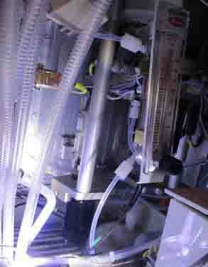
(4) Multi level process chambers
Chemical cabinet
Load port
FFU and exhaust
Chemical dispense system
Operating system: Windows NT
PC
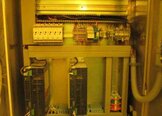
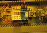
Power supply: 400 V, 75 A, 50/60 Hz
2005 vintage.
SEZ / LAM RESEARCH 4300 is a photoresist inhibitor equipment designed to assist semiconductor manufacturers in the lithography process. It is a high precision equipment used to identify and precisely dose the photoresist used in lithography processes. SEZ 4300 uses patented algorithm-based process control to scan, identify and precisely dose photoresists in one integrated unit. It can be easily integrated into existing lithography system workflow. LAM RESEARCH 4300 unit allows for a wide variety of photoresist applications, from deep ultra violet (DUV) to electron beam (EB). It is composed of several components, including a light source, a photoresist applicator, a substrate table, and a controller module. The light source provides a steady and uniform light image across the entire substrate for a uniform photoresist distribution. The photoresist applicator is composed of dispense valves, a dispense nozzles, and a dispense head that allow for precise control of the photoresist dispense process. The substrate table supports the substrate prior to exposing it to the light source. In addition to providing accurate and reliable photoresist application, the machine also has other beneficial features. It has an onboard vision tool that can detect any irregularities on the substrate surface, thus ensuring high quality results. Its automatic substrate recognition asset can quickly identify the substrate dimension and pattern prior to exposure. Its onboard data logging model provides extensive data and statistical analysis of the process. 4300 is a state-of-the-art photoresist inhibitor equipment designed to give manufacturers greater control and flexibility in their lithography process. It can dramatically reduce photoresist consumption and improve yield rates, resulting in increased efficiency and cost savings for semiconductor manufacturers.
There are no reviews yet
