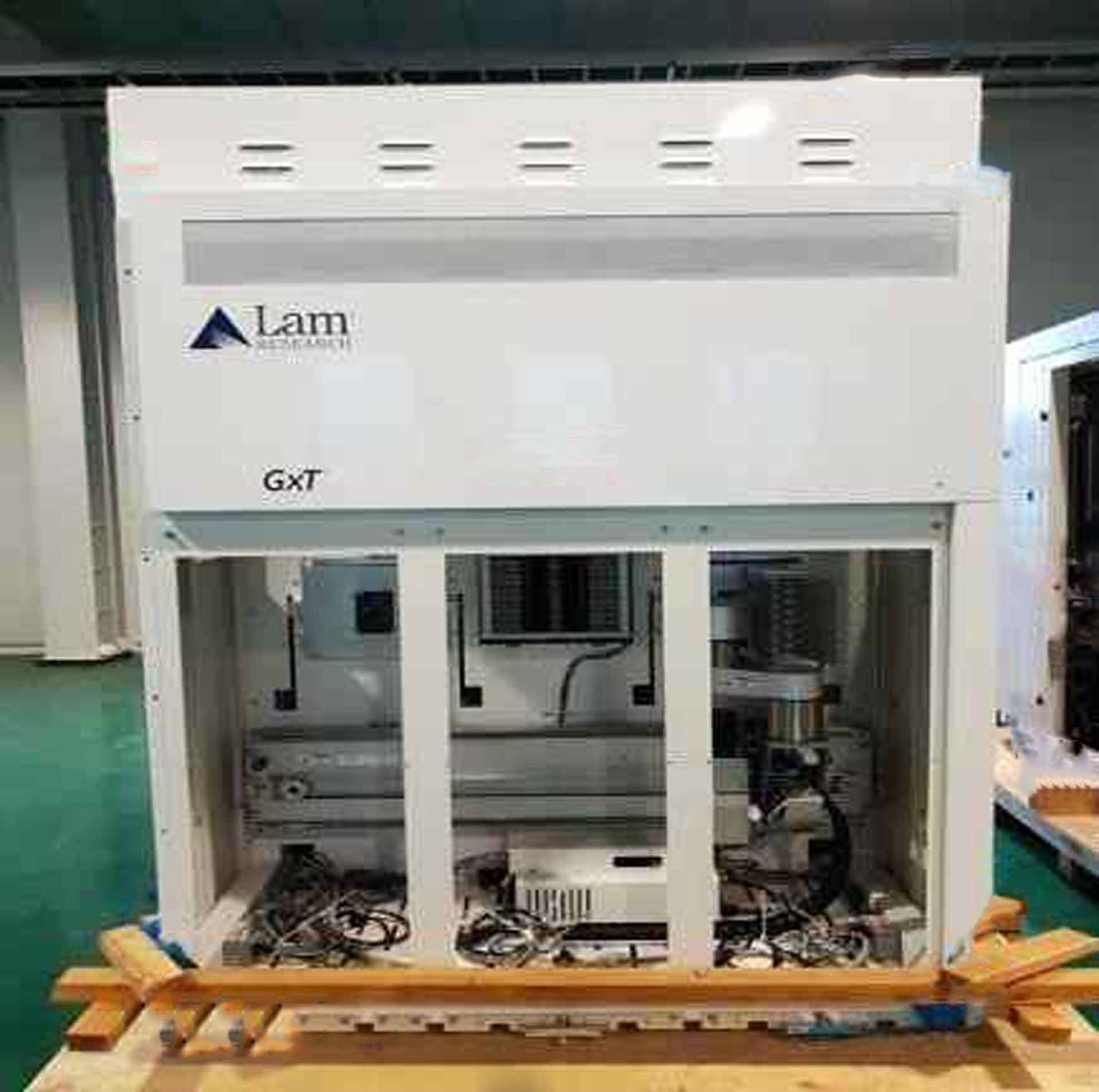
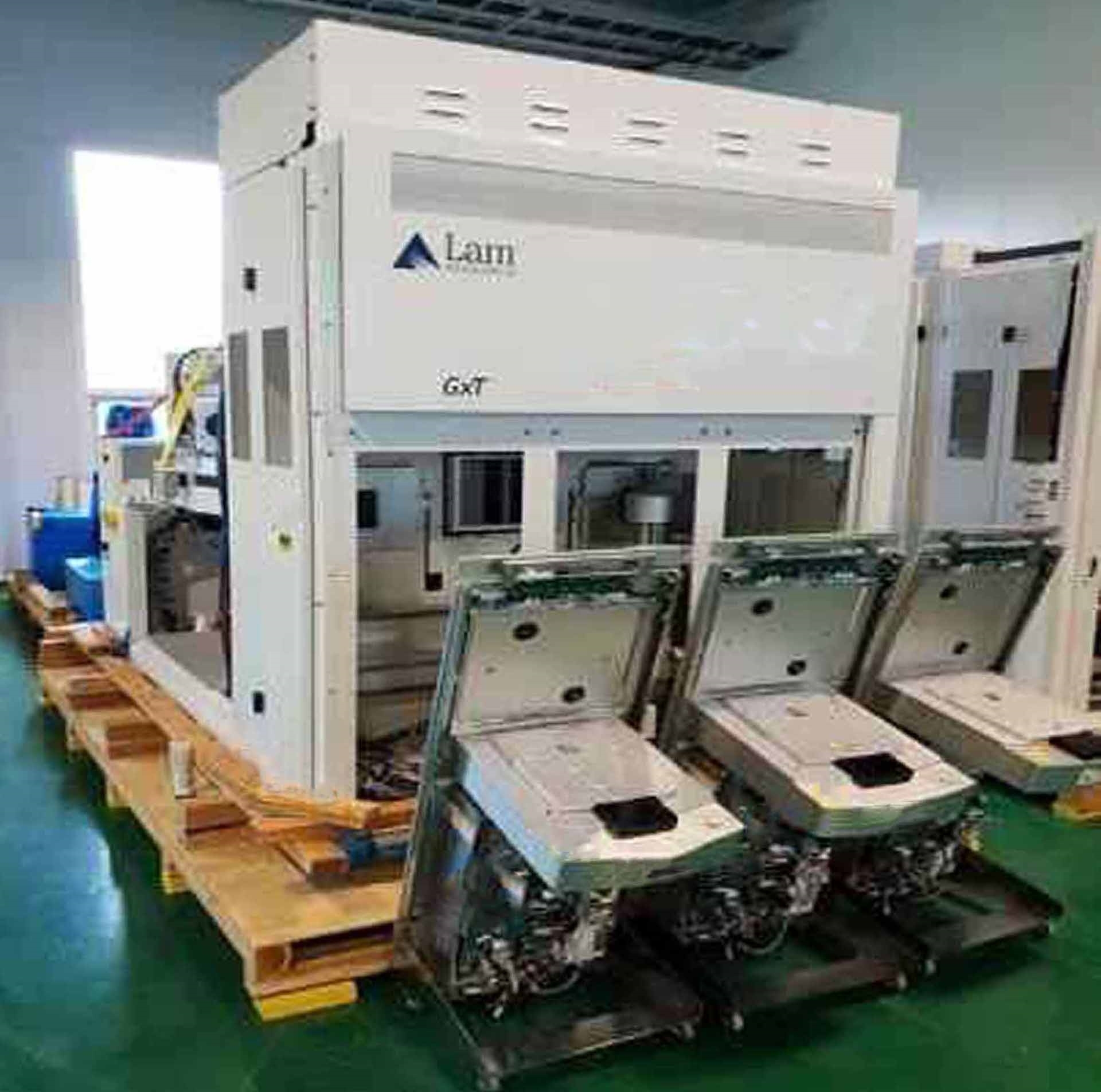
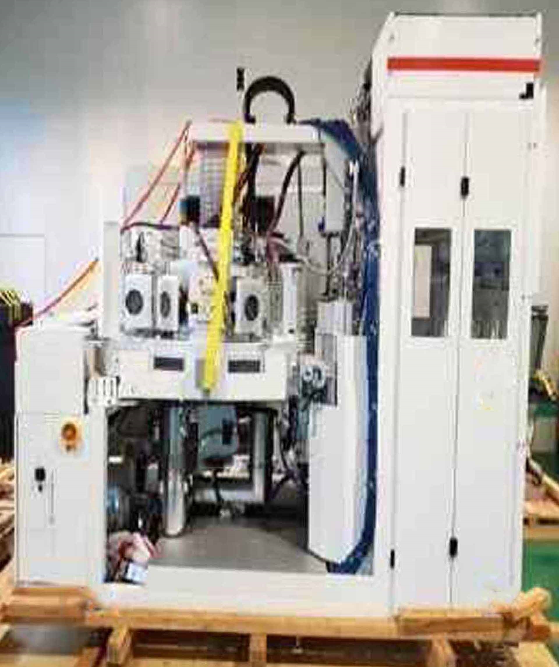
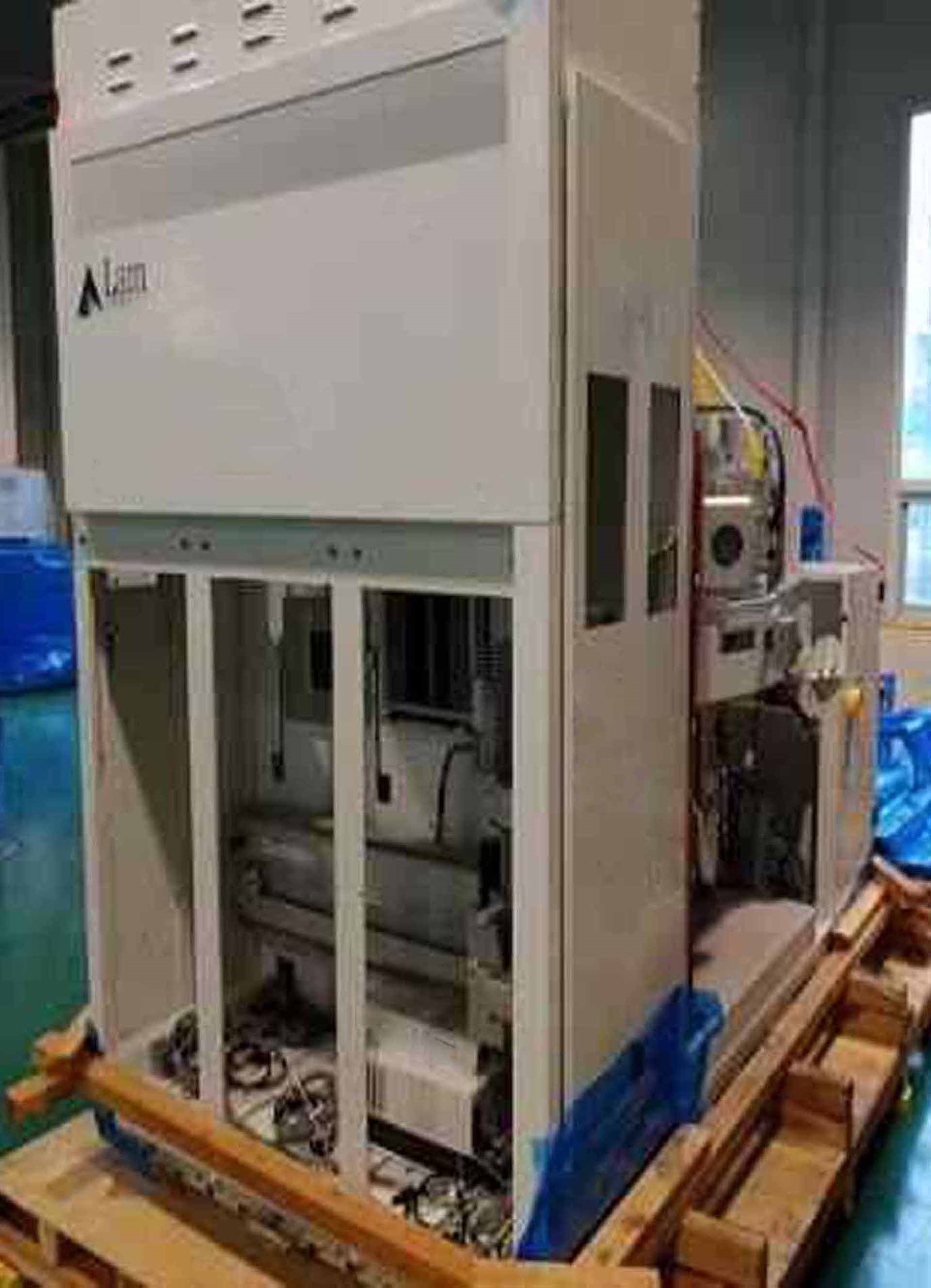
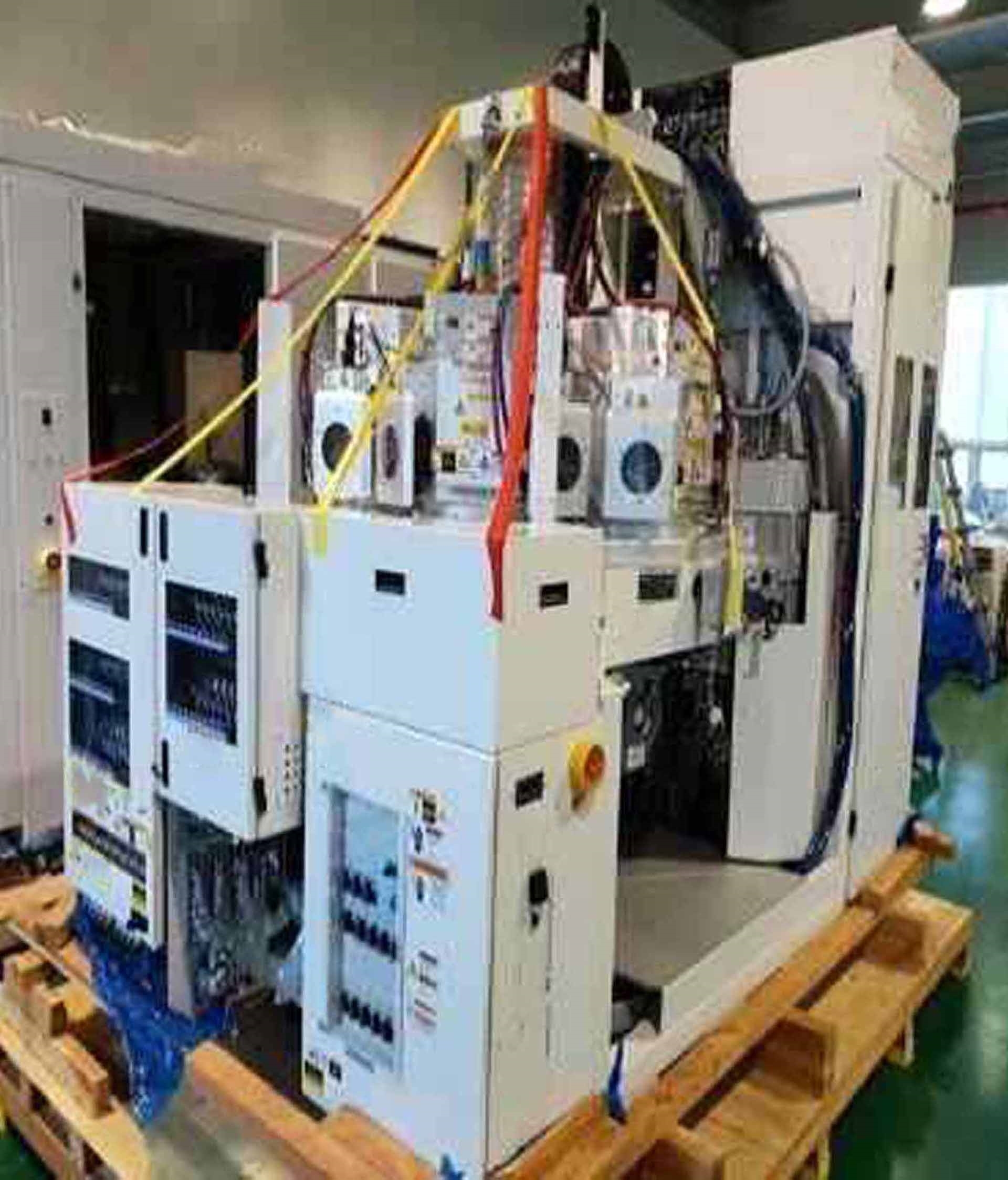
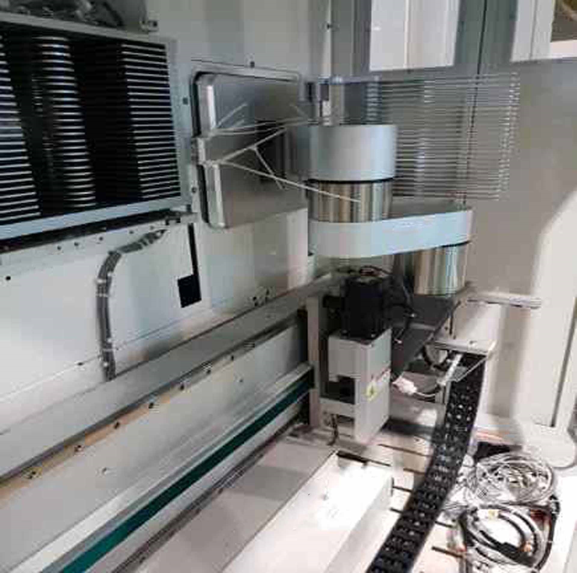
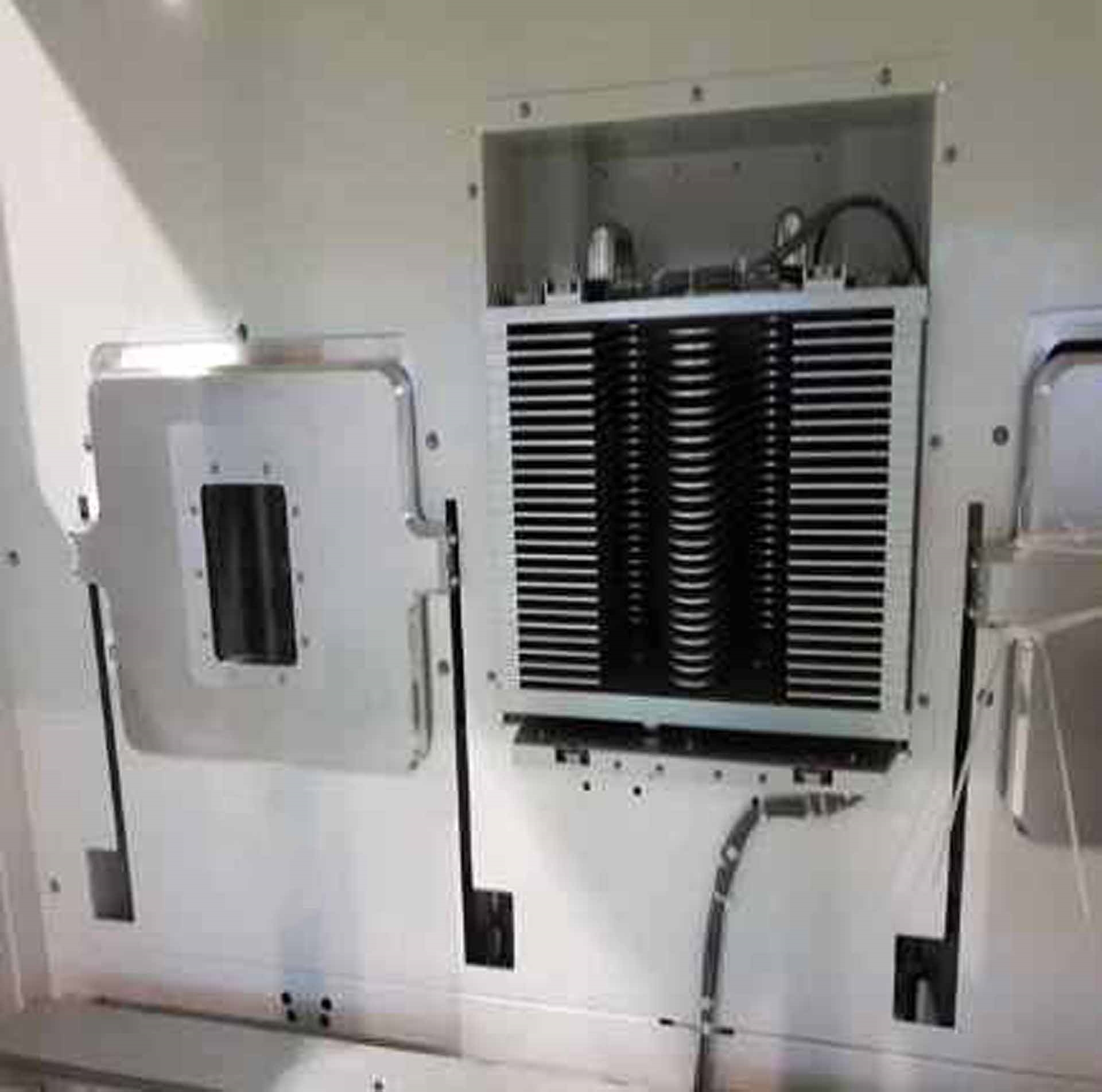
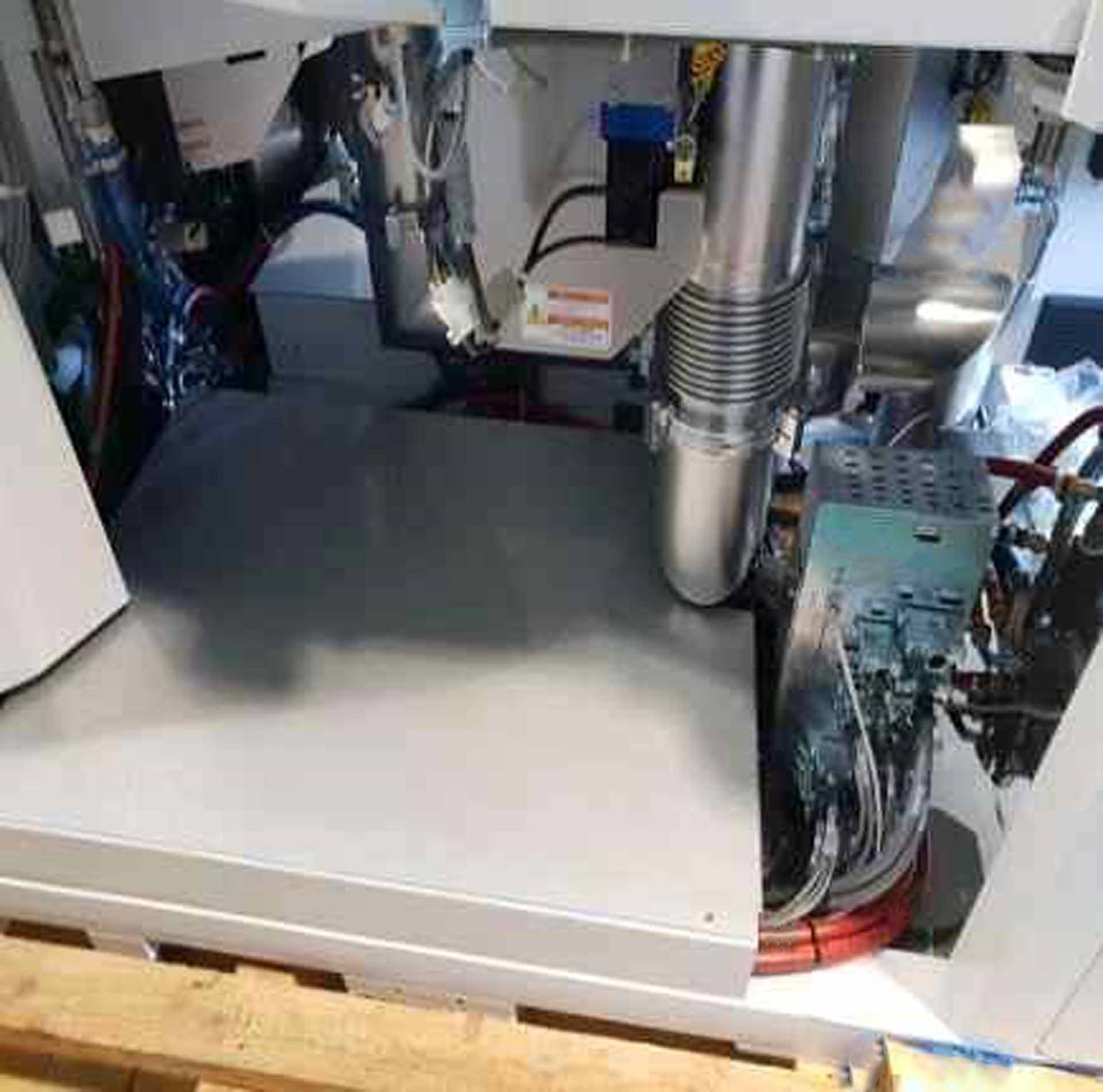
Used SEZ / LAM RESEARCH Gamma GXT #9226988 for sale
URL successfully copied!
Tap to zoom











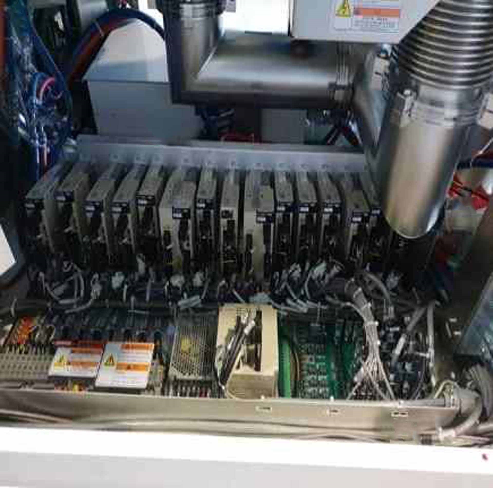

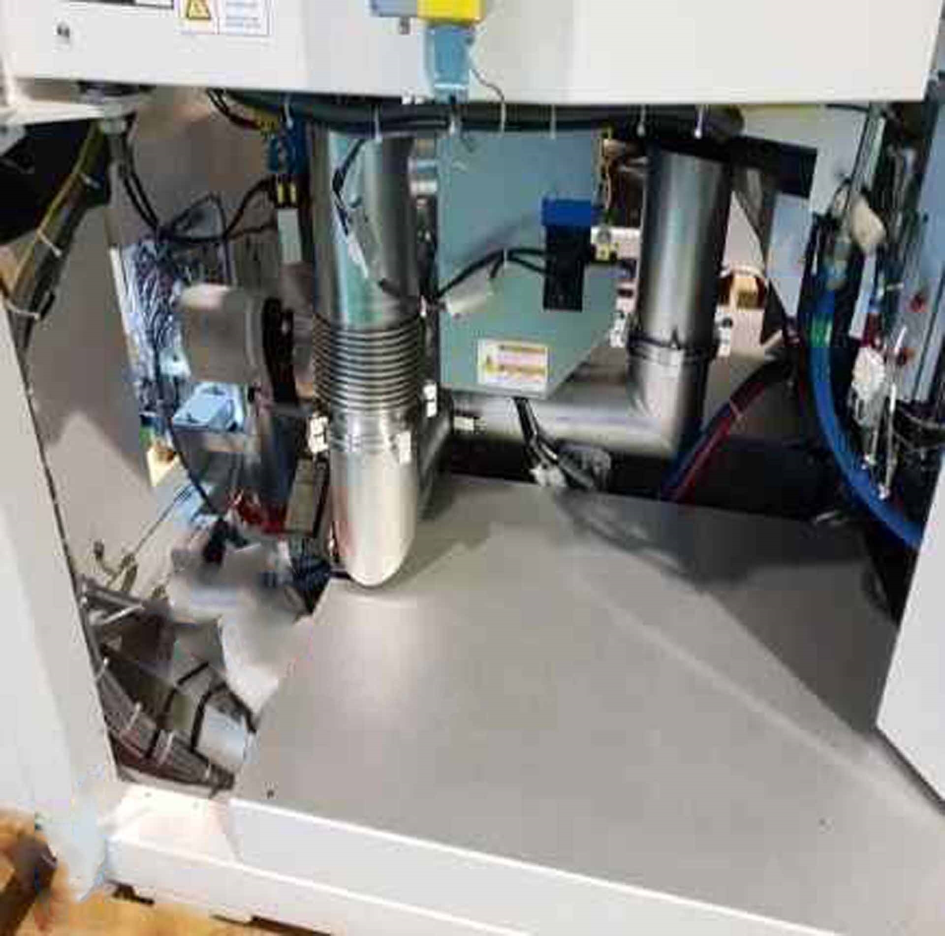



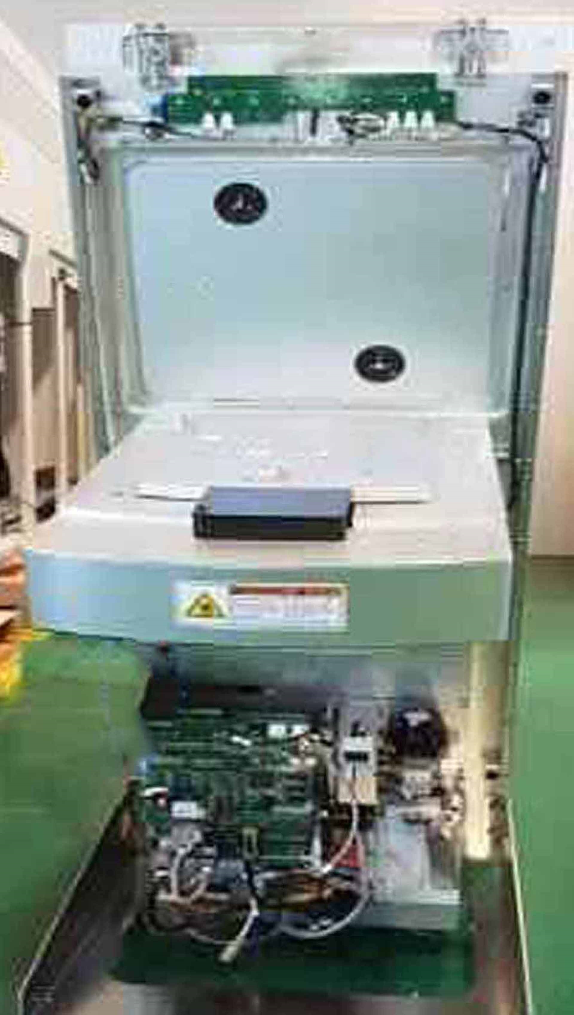

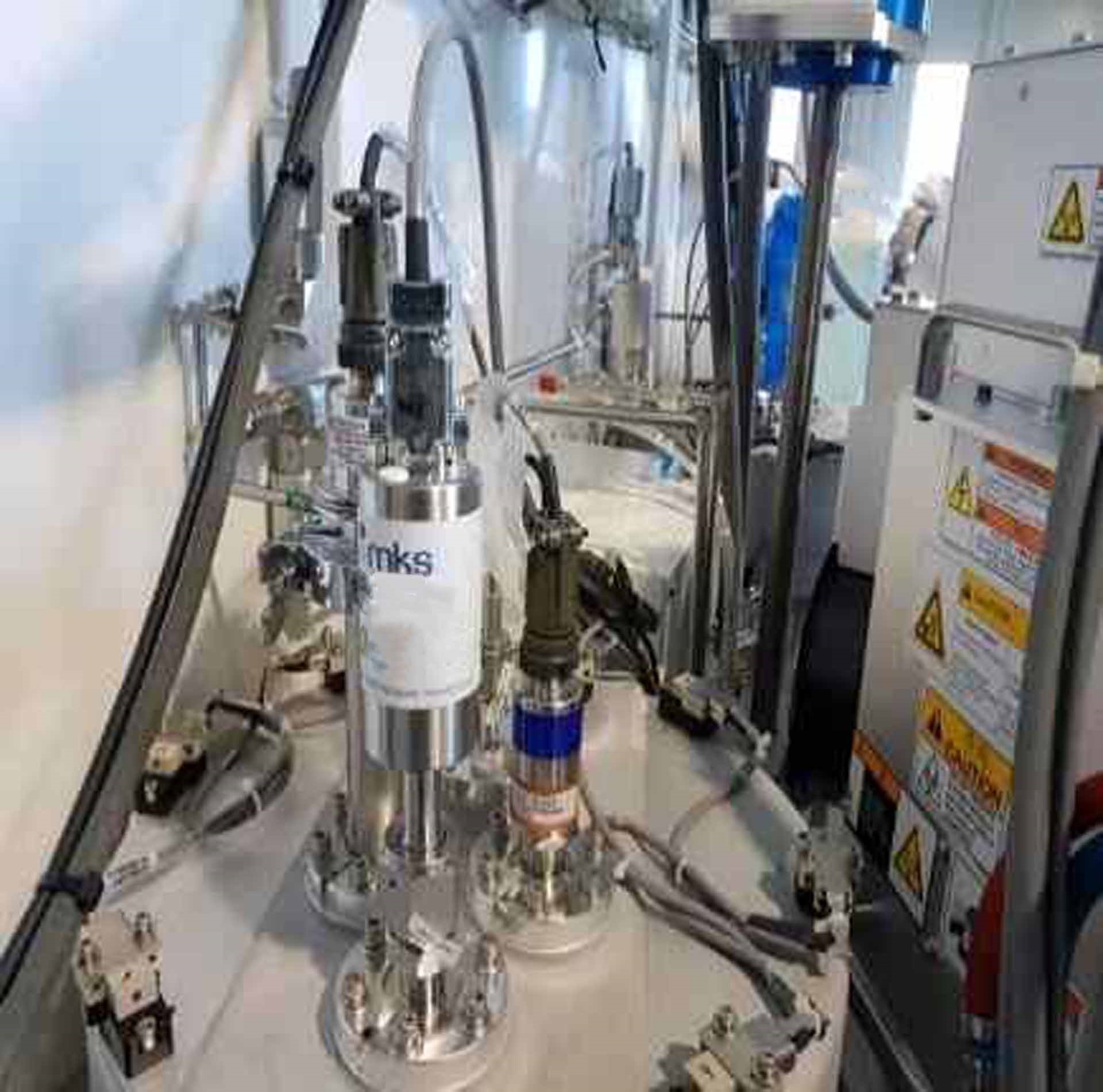



























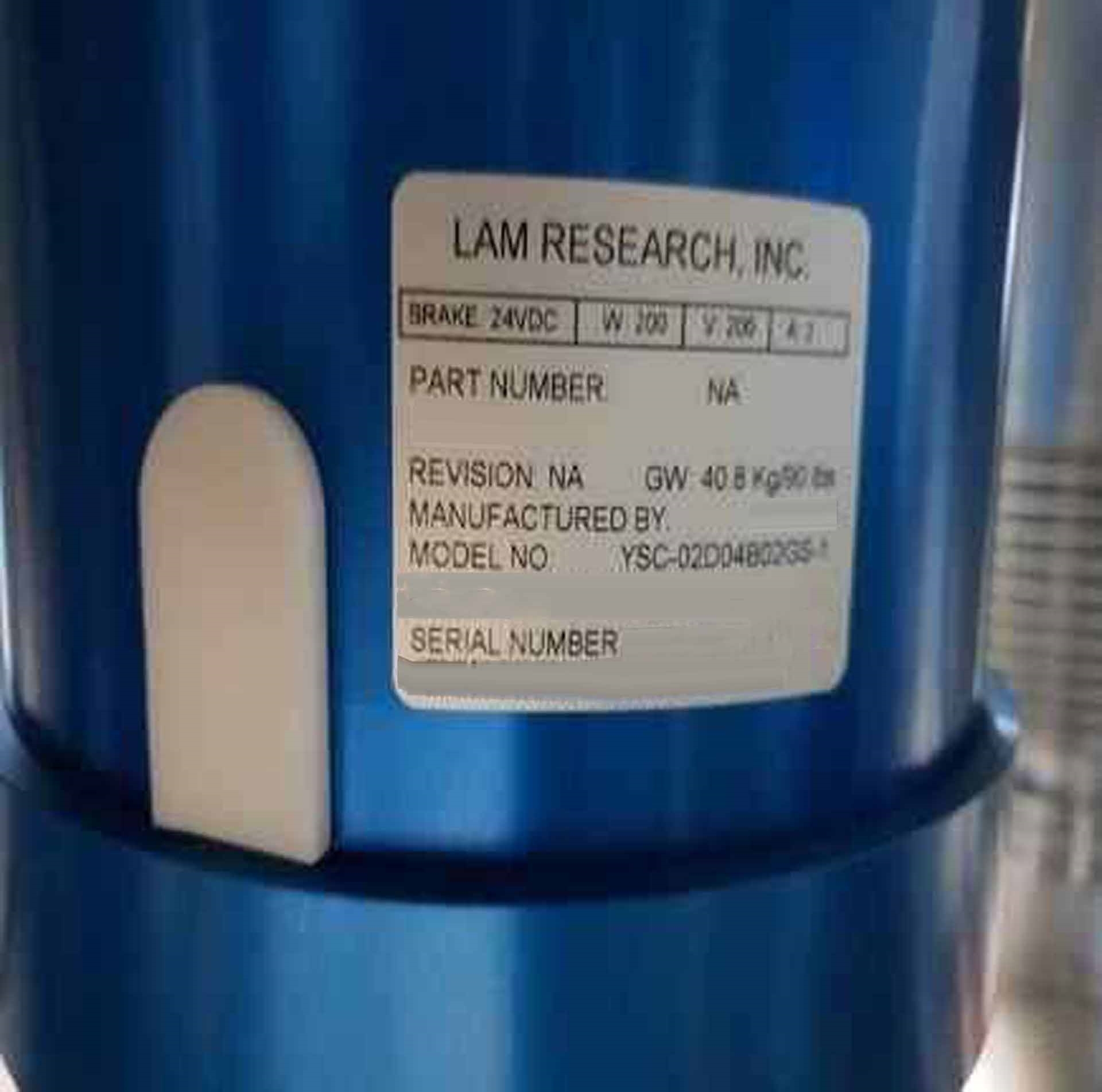

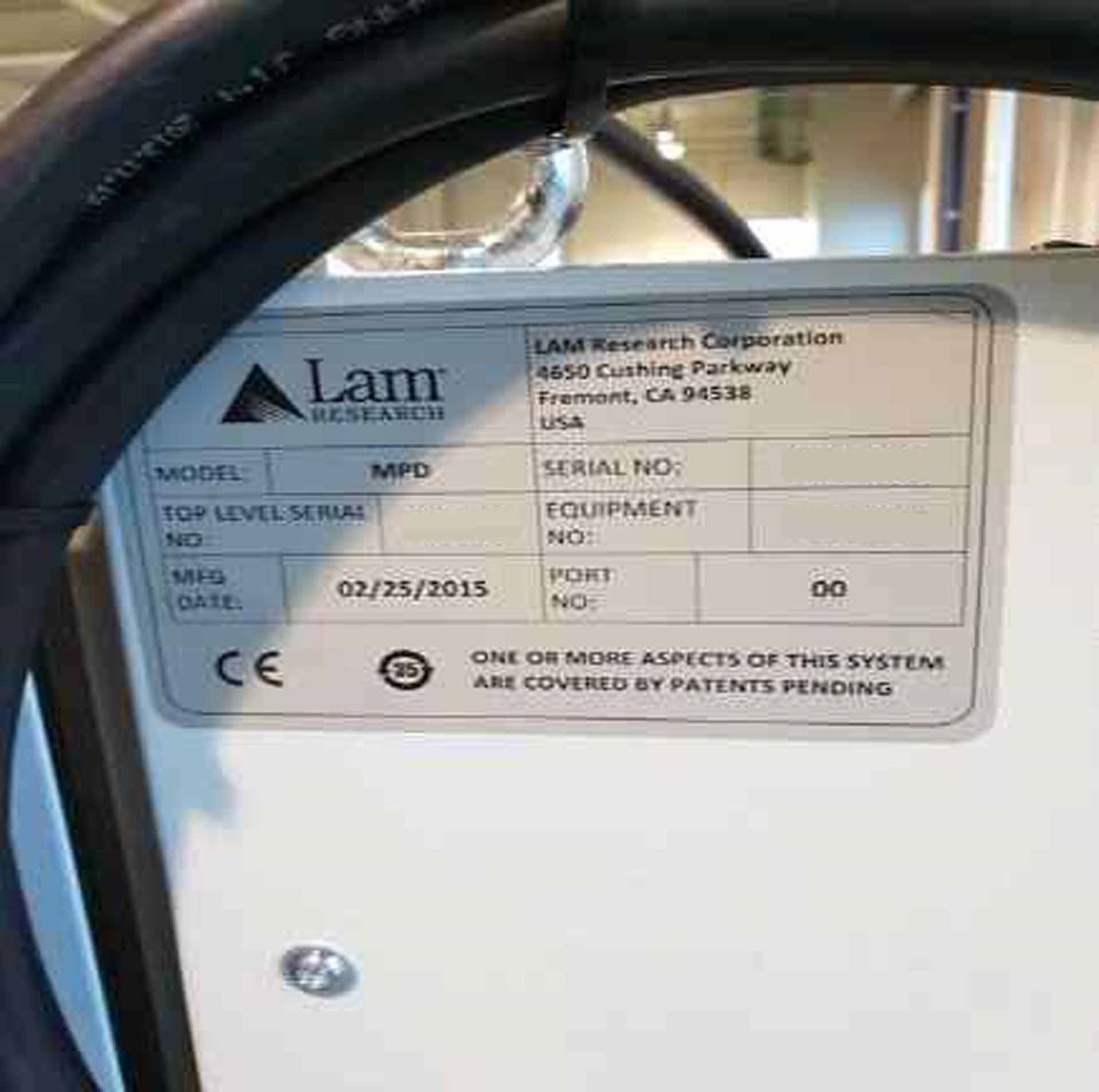

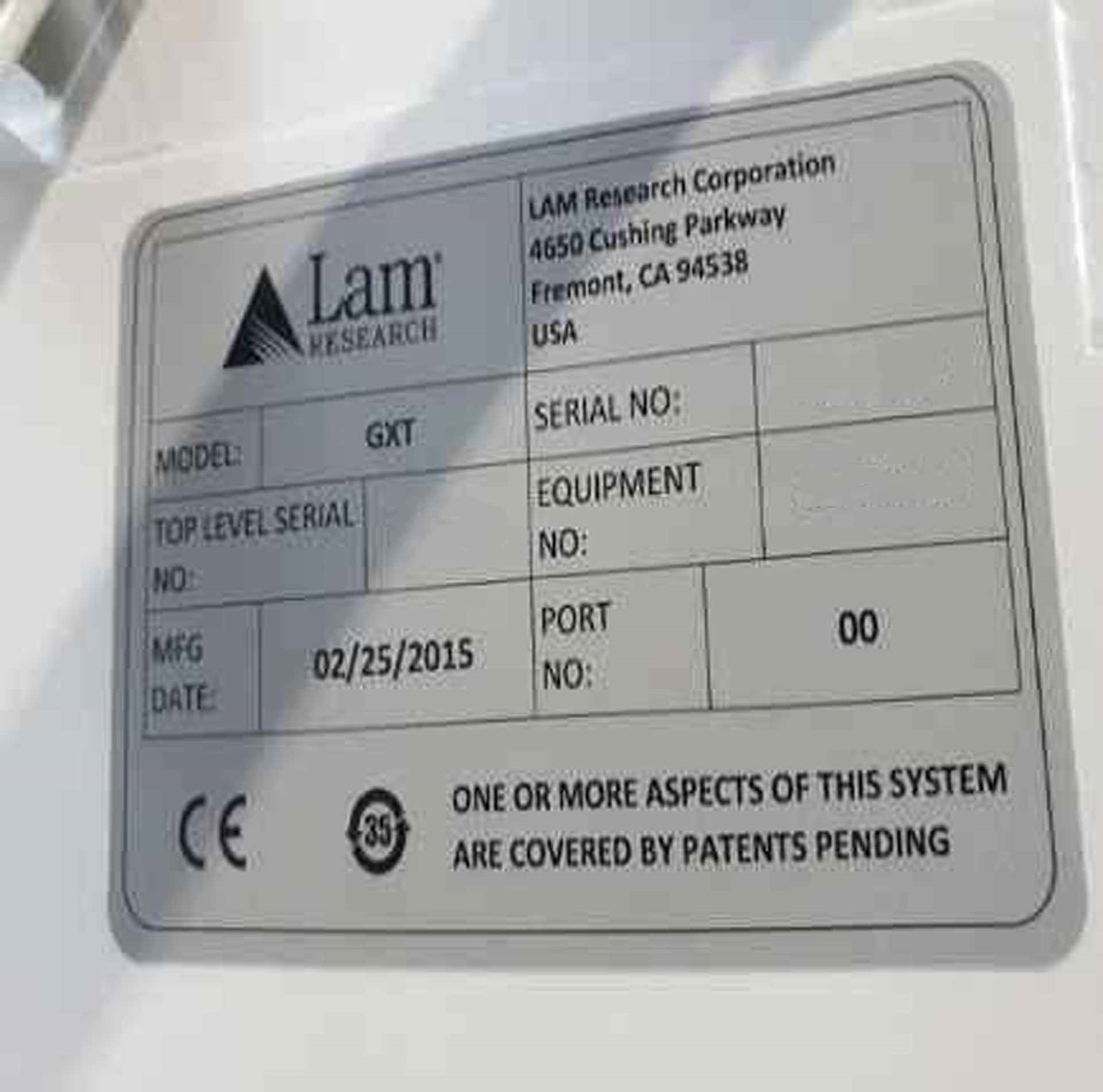

ID: 9226988
Wafer Size: 12"
Vintage: 2015
Photoresist stripper, 12"
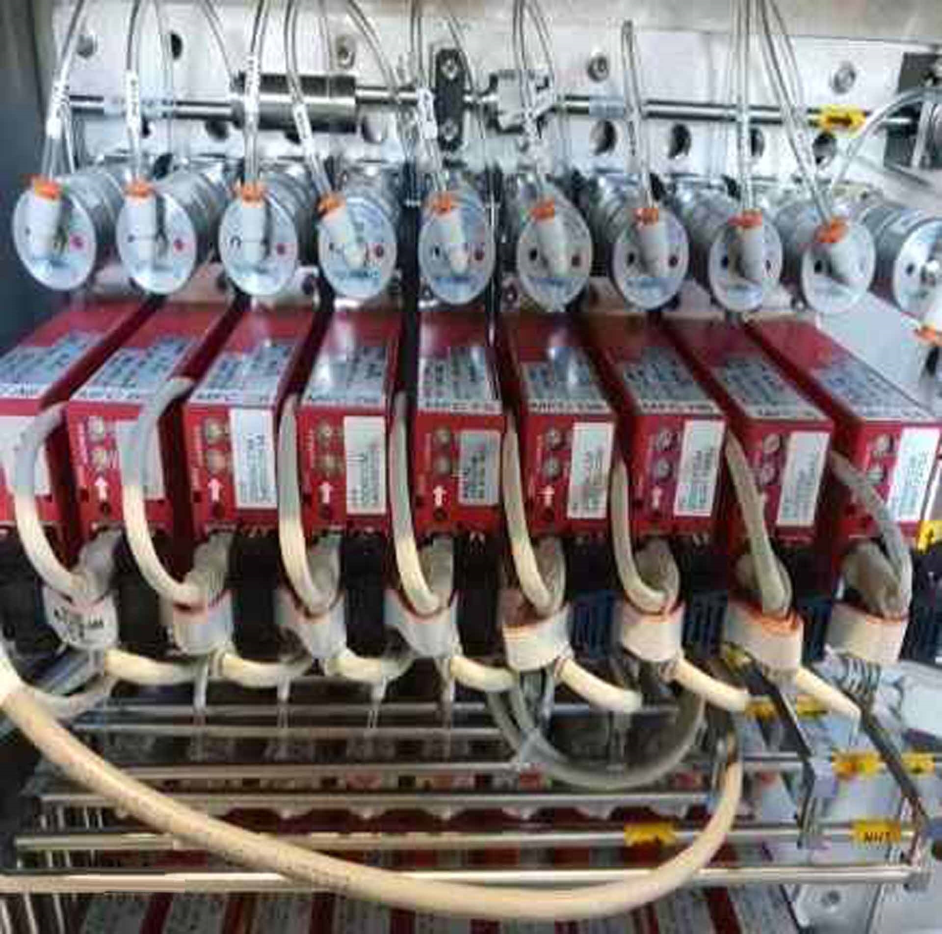
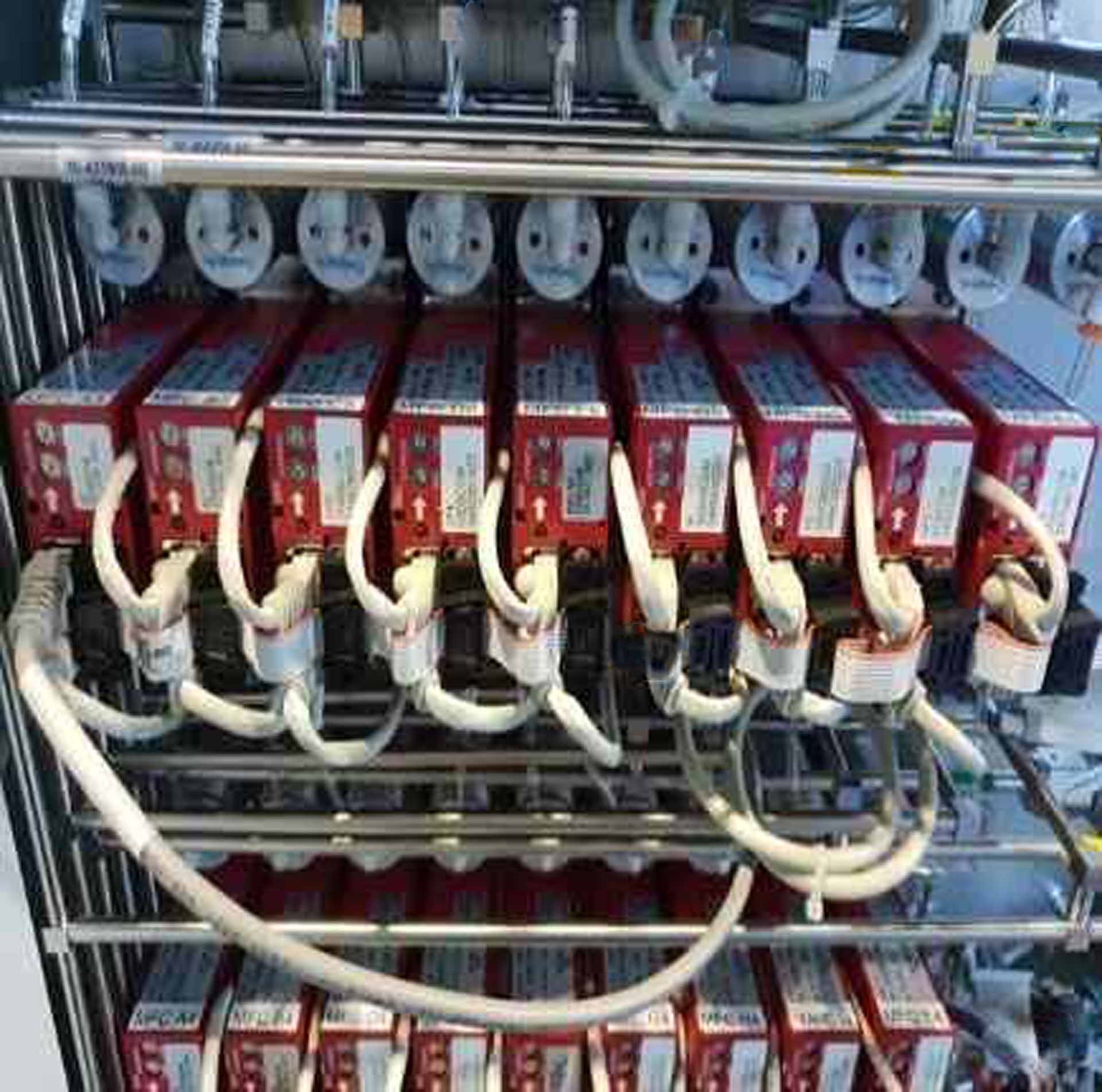
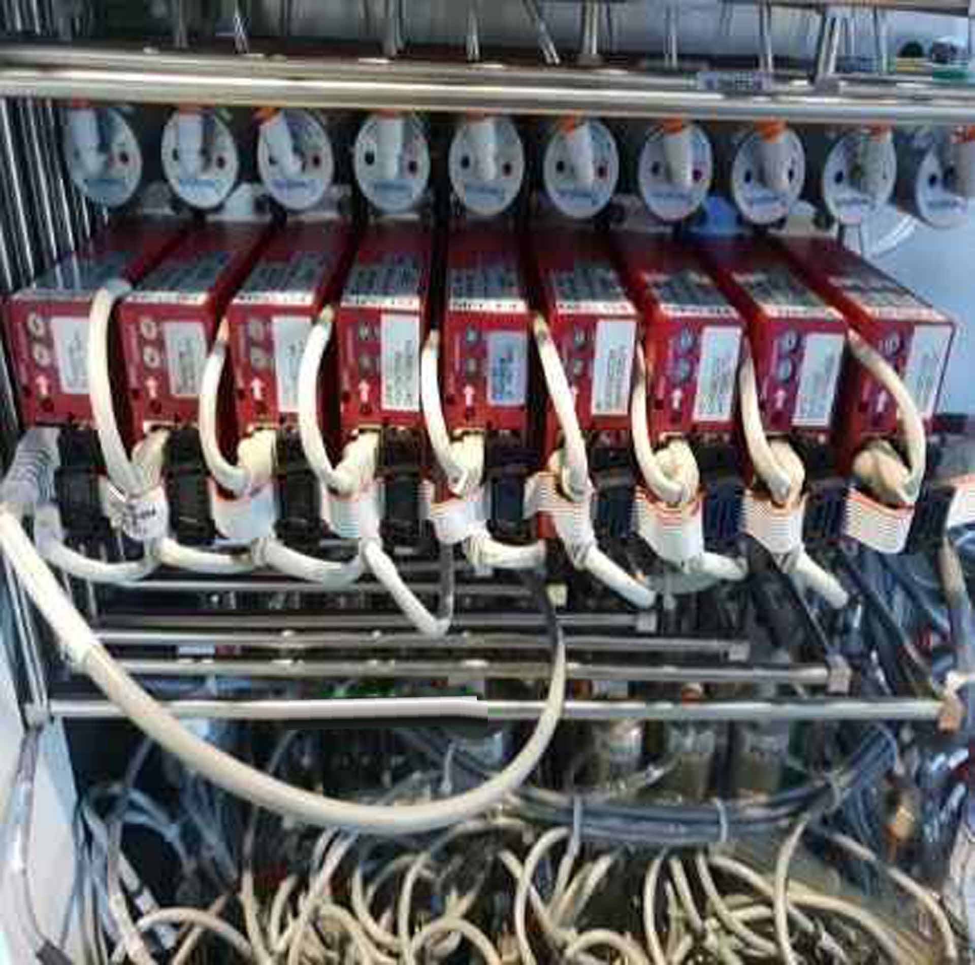
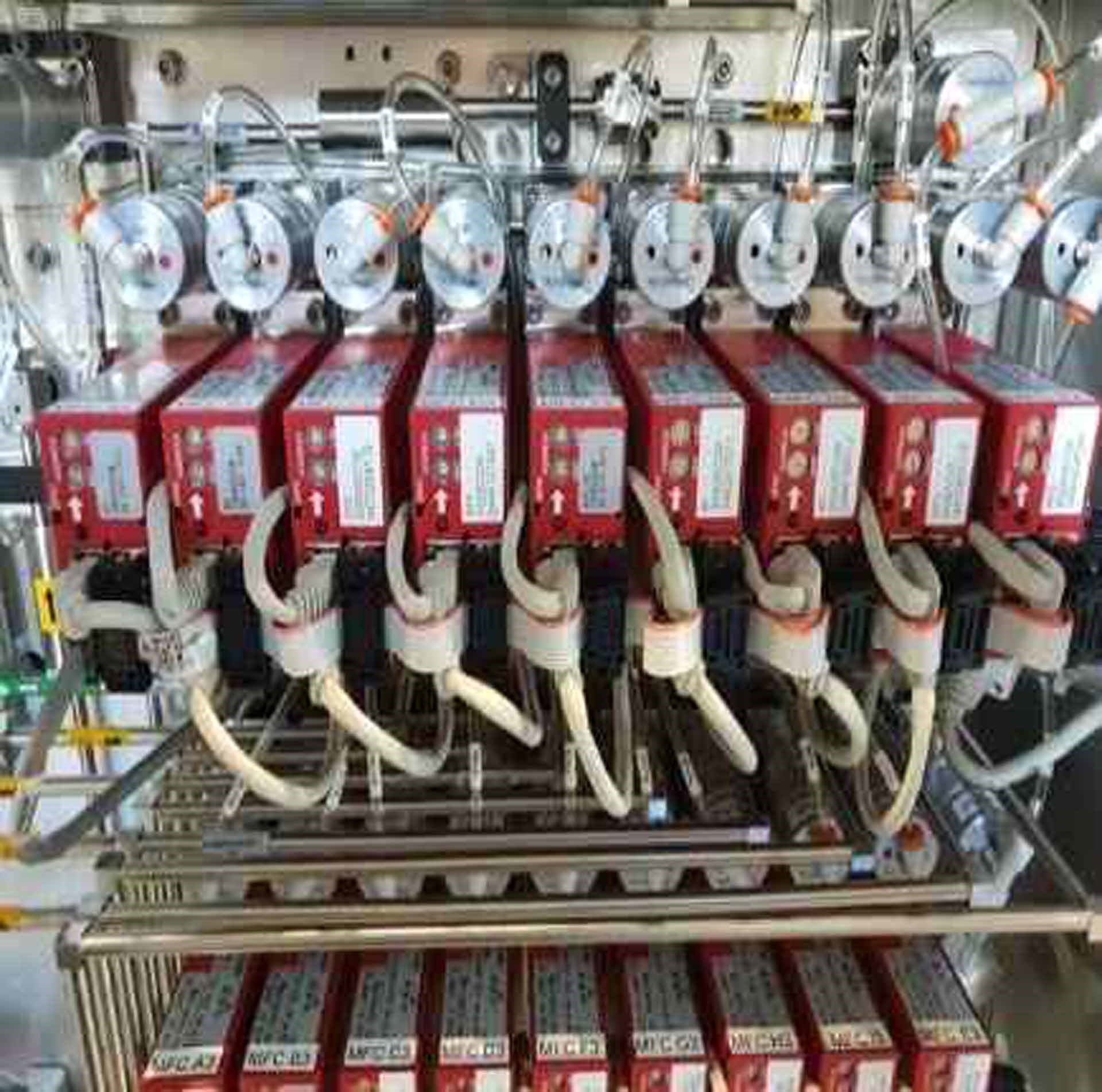
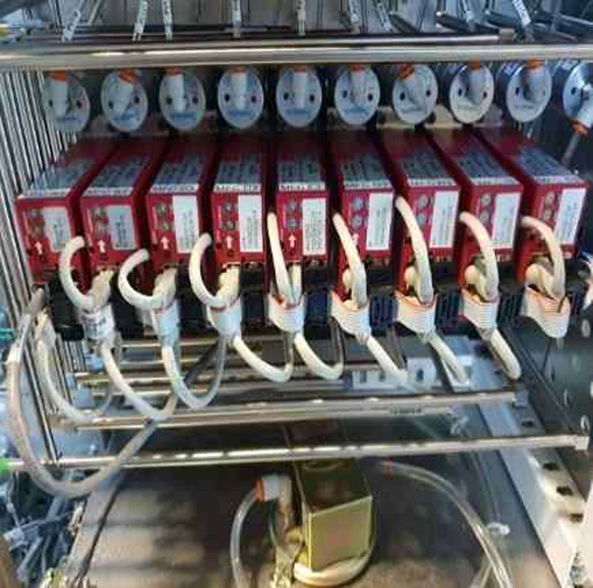
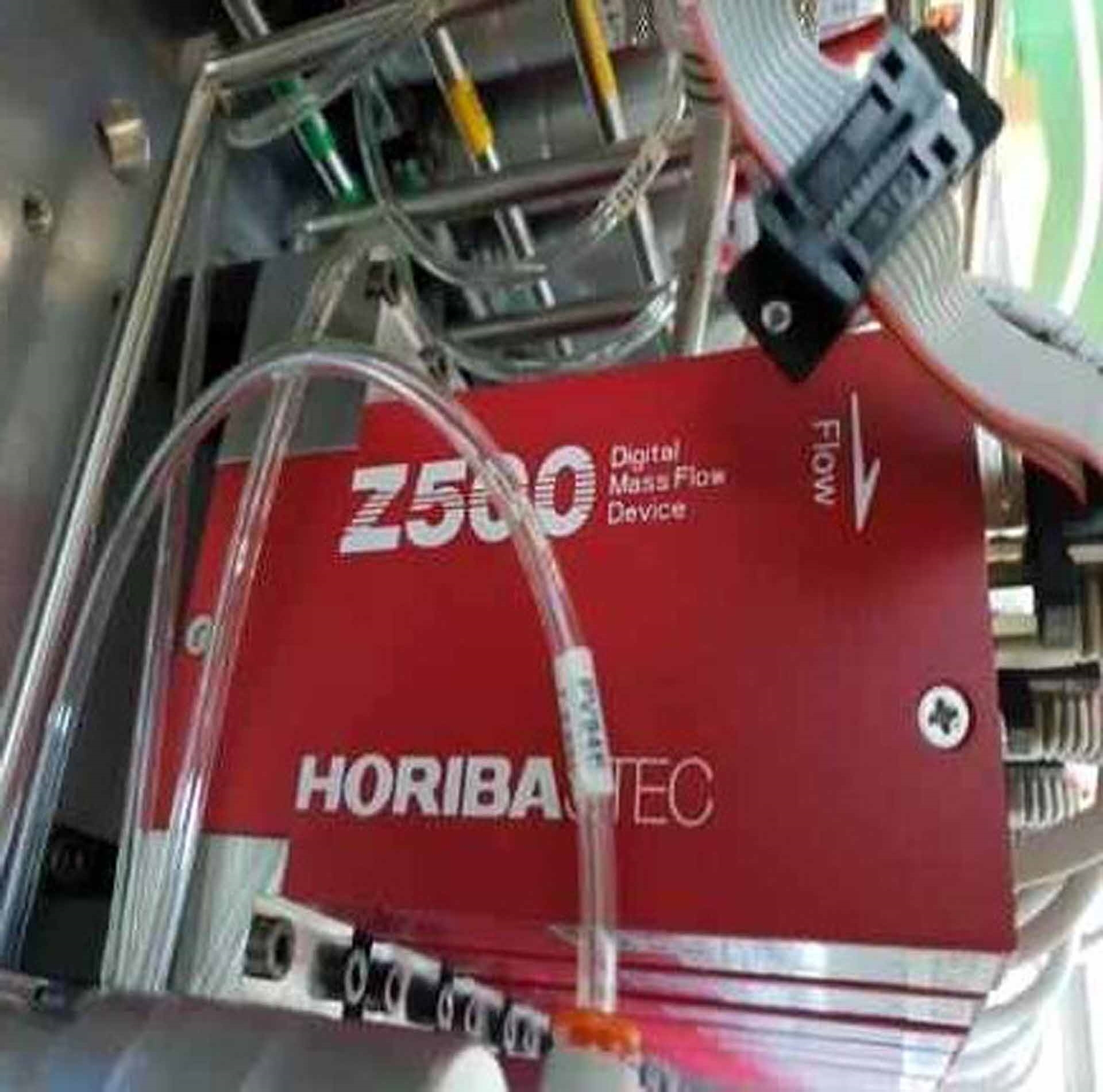
MFC: HORIBA Z500
Gases:
O2: 10000 SCCM
N2: 10000 SCCM
CO2: 2000 SCCM
CF4: 100 SCCM
AR: 3000 SCCM
4%H2/N2: 10000 SCCM
H2: 5000 SCCM
NF3: 50 SCCM
NH3: 5000 SCCM
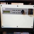
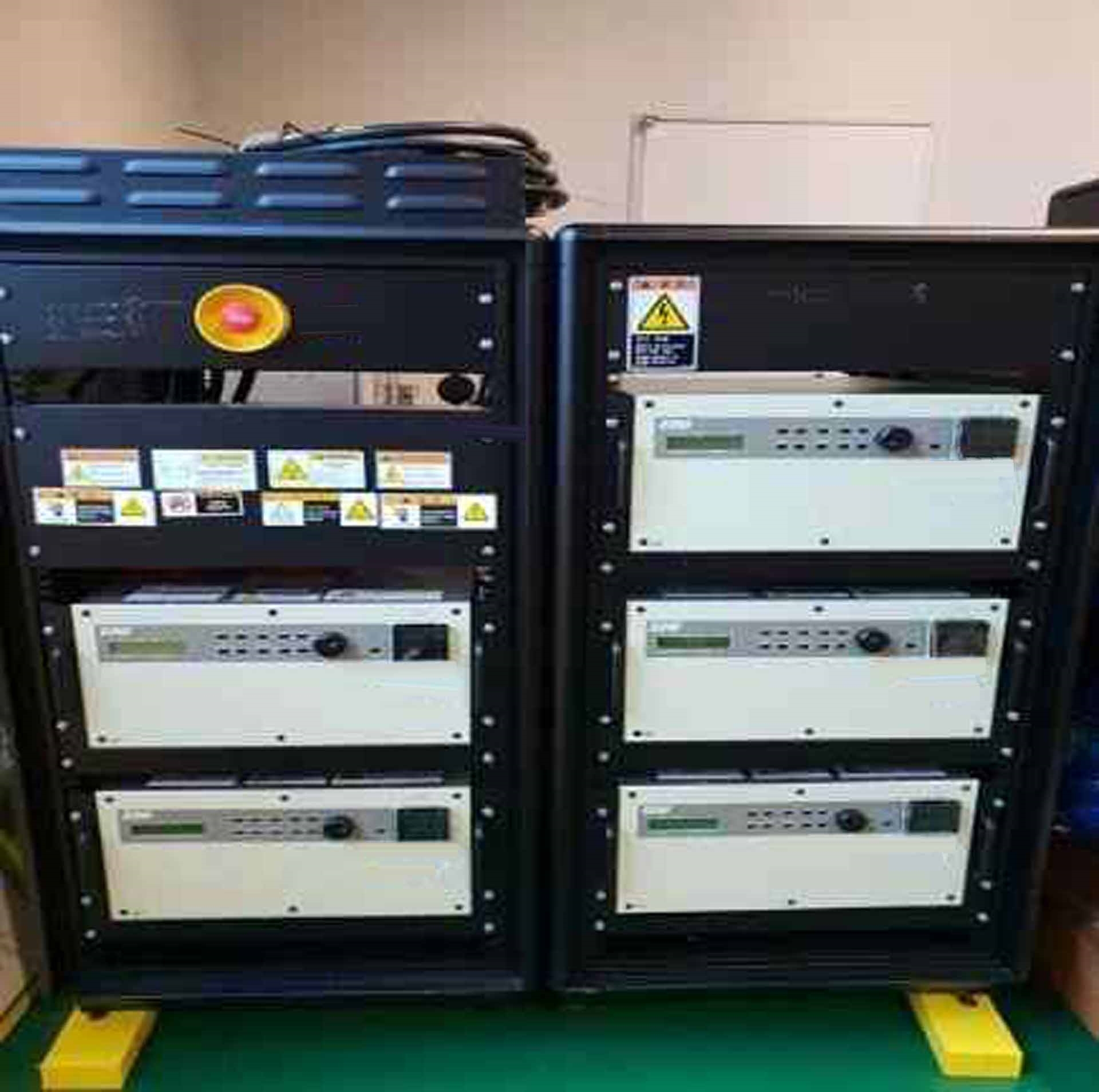
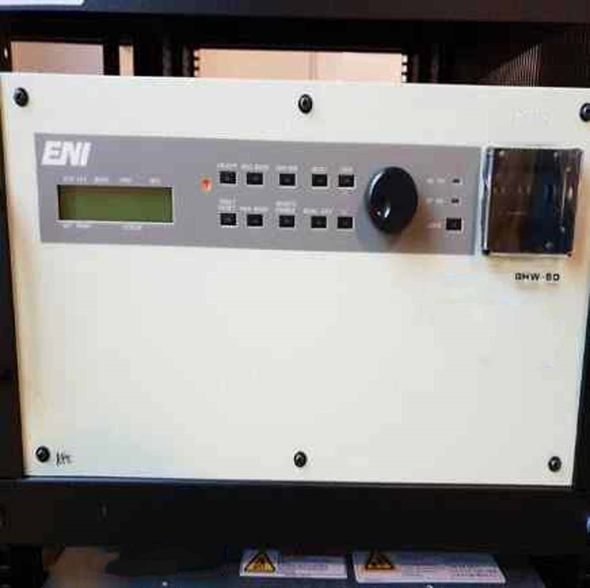
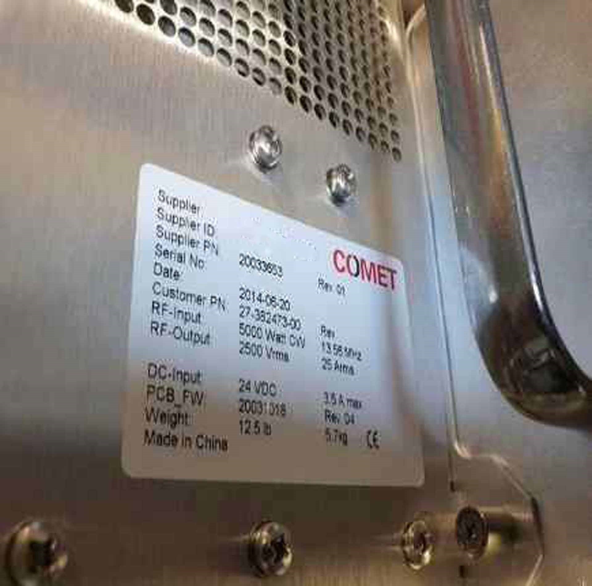
ENI GHW-50 RF Generator
MPD
Load port
2015 vintage.
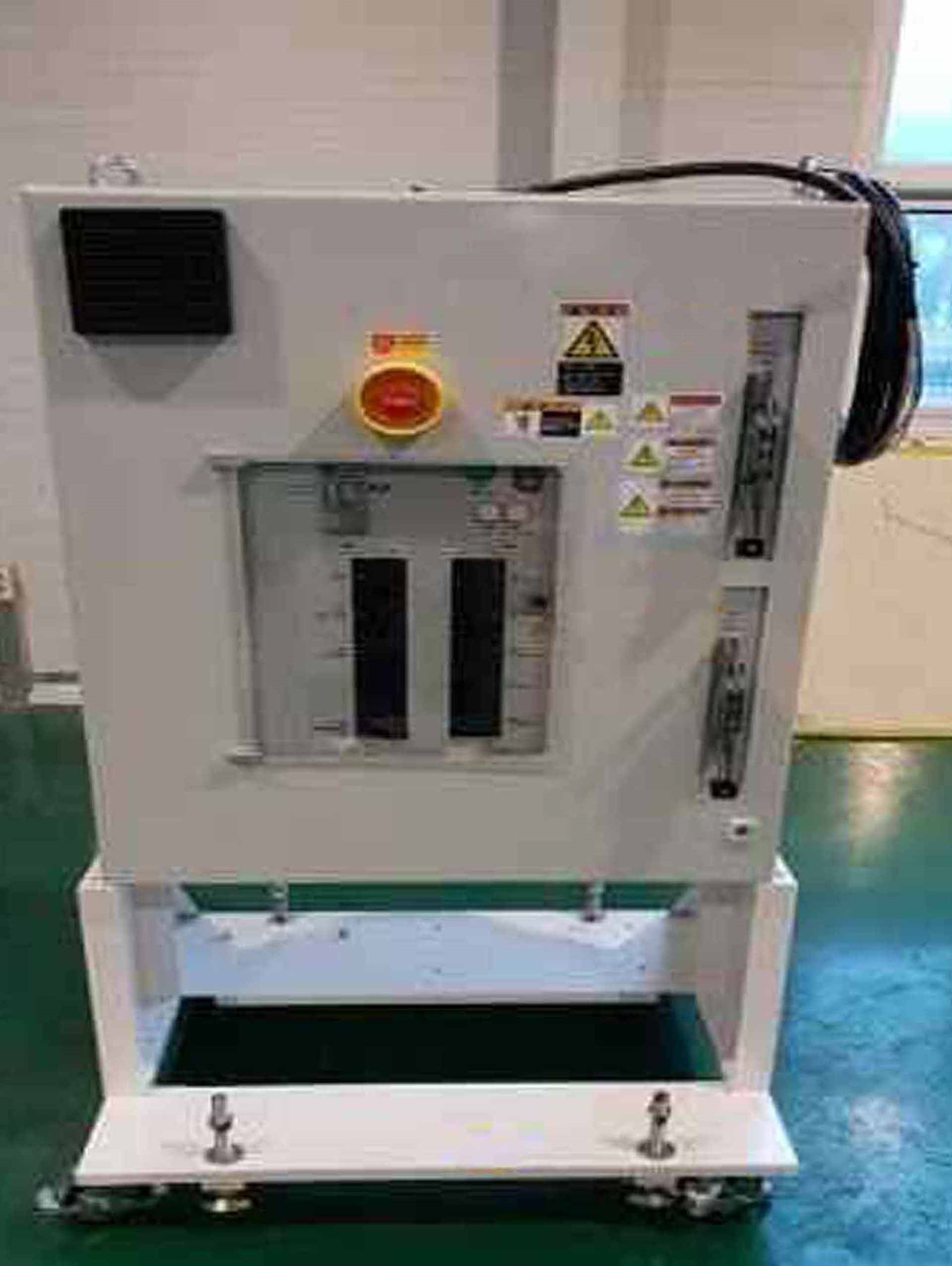
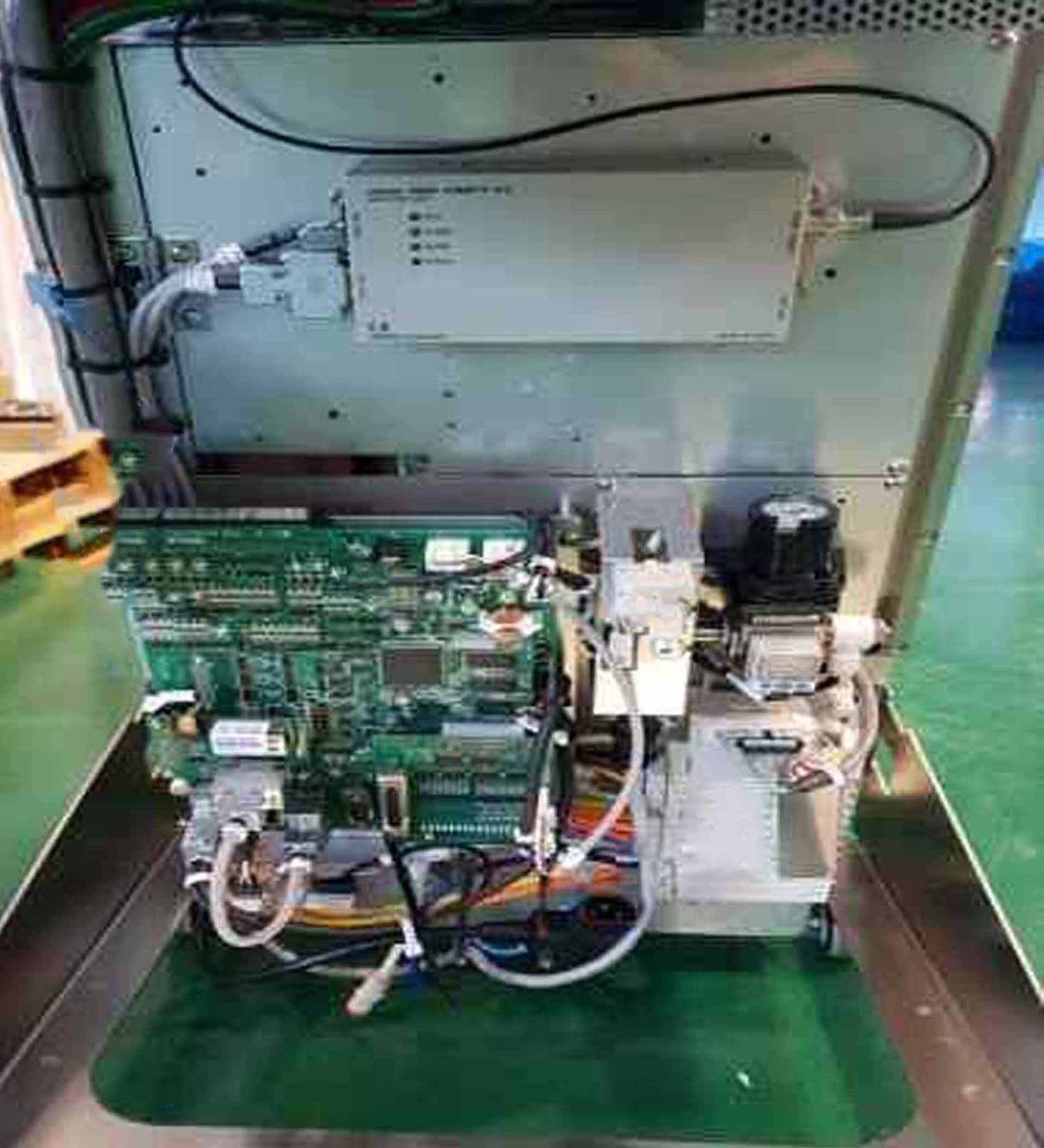
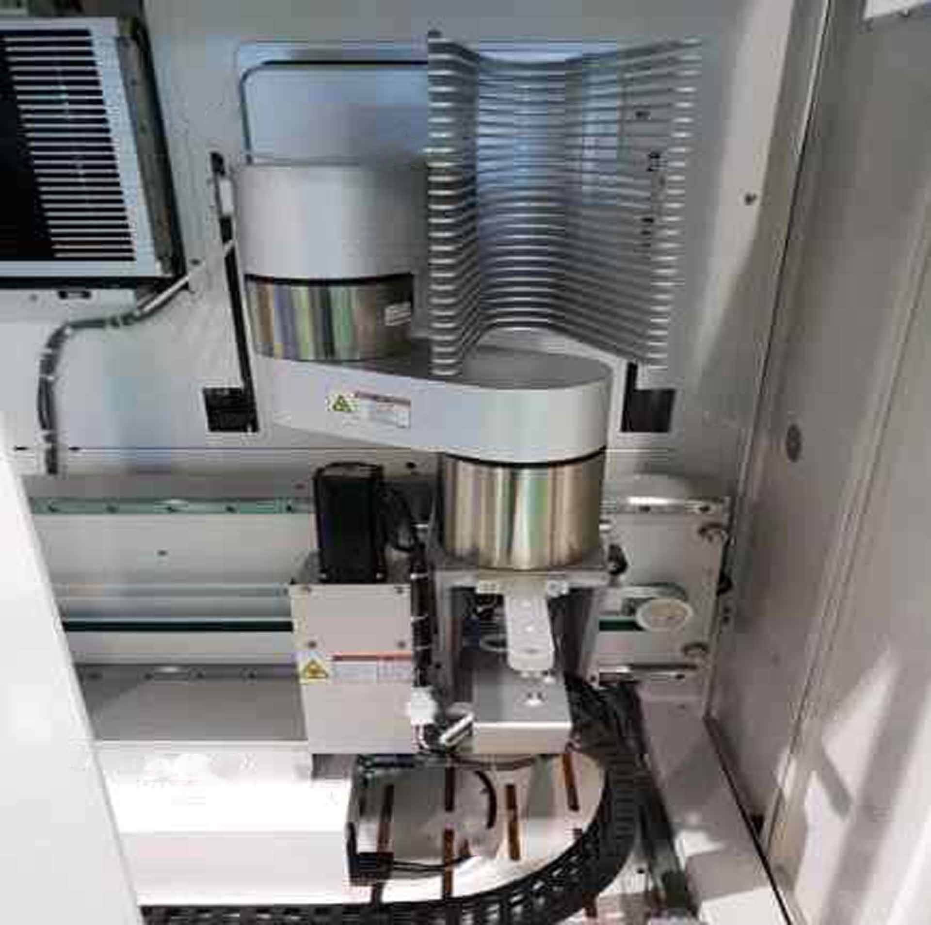
SEZ / LAM RESEARCH Gamma GXT is a photoresist equipment used to complete applications such as mask fabrication, pattern transfer, and other sensitive processes which require precision control over the exposure of thin layers of photoprocessable material to light sources. It has been specifically designed to produce dependable processing and optimize yield, both on production and R&D module configurations. This system features proprietary software, controls, and hardware SEZ has tailored specifically for its intended applications. At its core, a SEZ Gamma GXT type photoresist unit functions by effectively exposing thin layers of photoprocessable material to incident ultraviolet (UV) light or electron beams to modify its chemical structure or properties. It typically consists of a resist coater, a photoresist developer, a light source, a lens machine, and a wafer stage. LAM RESEARCH Gamma GXT's resist coater is responsible for applying a uniform and accurate layer of photolayers on the substrate before patterning. This is accomplished by using special coating heads which produce a solid film, which can be precisely controlled by a combination of manual and user-adjustable parameters. Next, the wafers are placed on a motorized stage and moved to the photoresist developer. In this, mixing and chemical solutions will dissolve the exposed portions of the photoresist, thus forming the desired patterns. The developer requires users to manage the process parameters such as cycle times and temperature with great precision in order to create accurate patterns with tight tolerances. The light source is a crucial component of any typical Gamma GXT tool and is responsible for the exposure of the wafers to UV lights. It can be configured to match desired target wavelengths, pulse lengths, and energy level settings. An advanced optical assembly which comprises of focusing elements, lenses, and mirrors, as well as a shutter asset, is responsible for directing light onto the wafer stage. This ensures that only the selected area of the photoprocessable material is exposed to the light and the other areas remain unaffected. Finally, the wafer stage securely holds the substrate in position while the exposure process is taking place and must be synchronized with the movement of all other components in the model. SEZ / LAM RESEARCH Gamma GXT series offers a flexible and adjustable stage with a wide range of motion capabilities to meet varying processing needs. Overall, SEZ Gamma GXT is designed to provide precision, accuracy, and dependability during high-volume photoresist application processes. It boasts advanced automation capabilities, optimized processing quality, and superior environmental management, making it a reliable solution for most photomask production and development requirements.
There are no reviews yet
