Used SOLITEC 5100 #293774777 for sale
URL successfully copied!
Tap to zoom
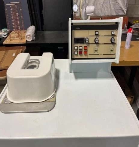

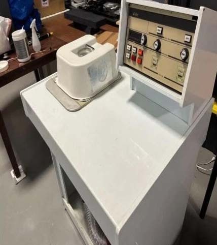
SOLITEC 5100 is a cutting-edge photoresist equipment used in the semiconductor industry for photolithography processes. This system is designed to meet the stringent requirements of advanced semiconductor manufacturing, offering high performance and reliability for producing precise and intricate patterns on semiconductor substrates. Photoresist materials are crucial in the fabrication of semiconductor devices as they act as a protective mask during the etching process, defining the areas where material will be removed or deposited. 5100 photoresist unit consists of a series of components and processes that work together to ensure the successful patterning of semiconductor wafers. The machine includes a photoresist coating unit, a soft bake module, an exposure tool, and a development module. Each component plays a critical role in the overall lithography process, contributing to the resolution, line-width control, and uniformity of the final pattern. The photoresist coating unit is responsible for applying a thin layer of photoresist material onto the surface of the semiconductor wafer. This step requires precise control over parameters such as spin speed, dispense rate, and coating thickness to achieve uniform coverage across the wafer. SOLITEC 5100 asset is equipped with advanced dispensing and spin coating technology to ensure consistent and reliable photoresist deposition. After the photoresist is coated onto the wafer, it undergoes a soft bake process to remove solvent and improve adhesion to the substrate. The soft bake module in 5100 model offers precise temperature control and ramp rates to ensure uniform baking and minimize defects in the photoresist film. Proper soft baking is essential for optimizing the sensitivity of the photoresist during the exposure step. The exposure equipment in SOLITEC 5100 uses advanced optics and alignment capabilities to pattern the photoresist layer according to the design layout. This step involves exposing the photoresist to ultraviolet (UV) light through a mask or reticle, transferring the pattern onto the wafer. The exposure parameters, such as light intensity, exposure time, and alignment accuracy, are critical for achieving high-resolution patterns and tight dimensional control. Following exposure, the wafer is transferred to the development module for the selective removal of exposed or unexposed regions of the photoresist. 5100 system offers precise control over the development process, including temperature, time, and chemistry, to ensure clean and well-defined pattern transfer. Proper development is essential for achieving the desired pattern fidelity and minimizing defects in the final semiconductor device. Overall, SOLITEC 5100 photoresist unit is designed to meet the demanding requirements of advanced semiconductor fabrication, offering high precision, reliability, and process control. By leveraging the capabilities of this machine, semiconductor manufacturers can achieve superior patterning results with excellent resolution, line-width control, and uniformity, ultimately leading to the production of high-performance semiconductor devices.
There are no reviews yet