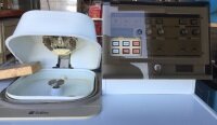
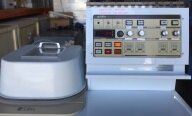
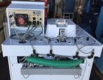
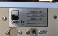
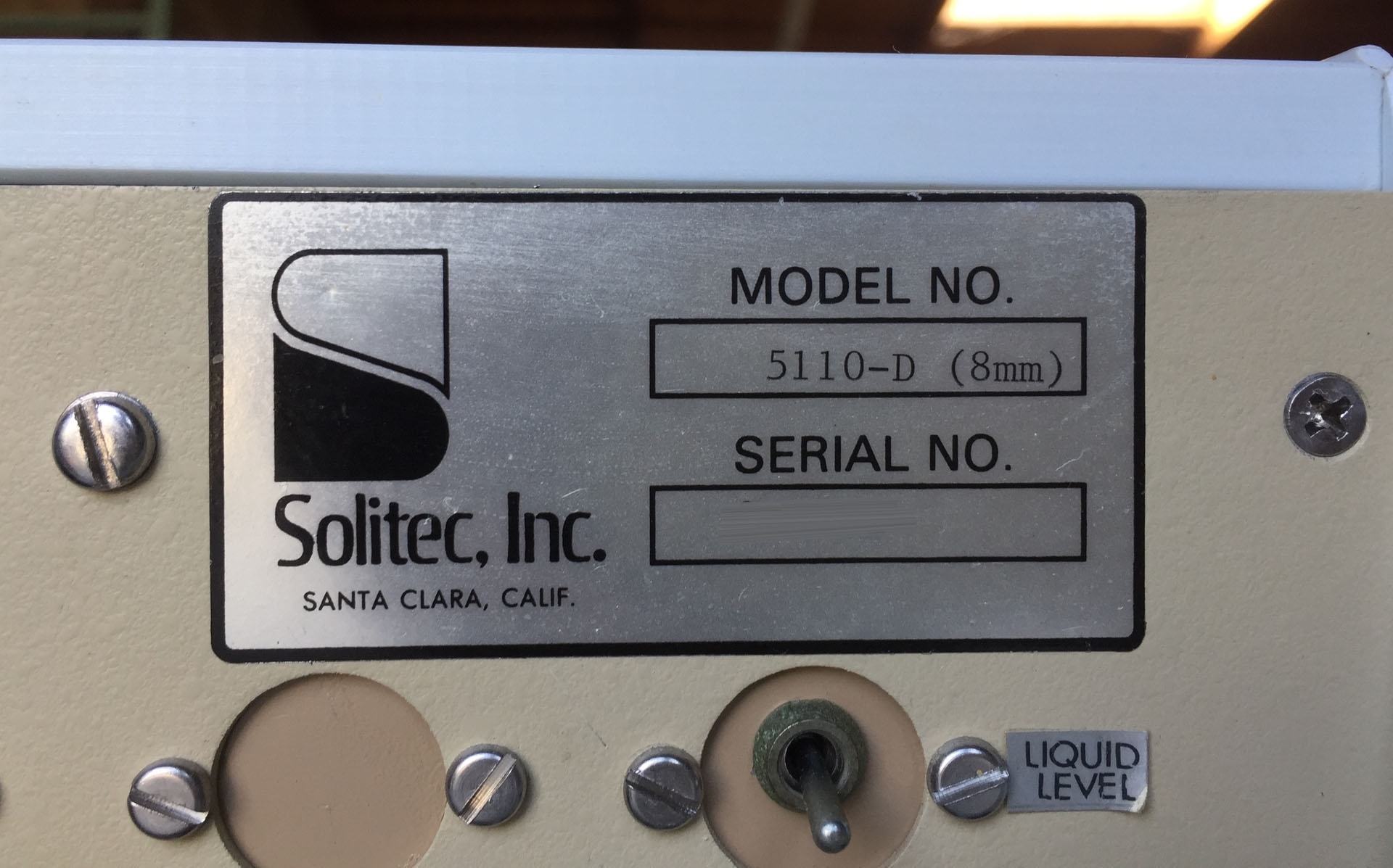
Used SOLITEC 5110-D #9270248 for sale
URL successfully copied!
Tap to zoom
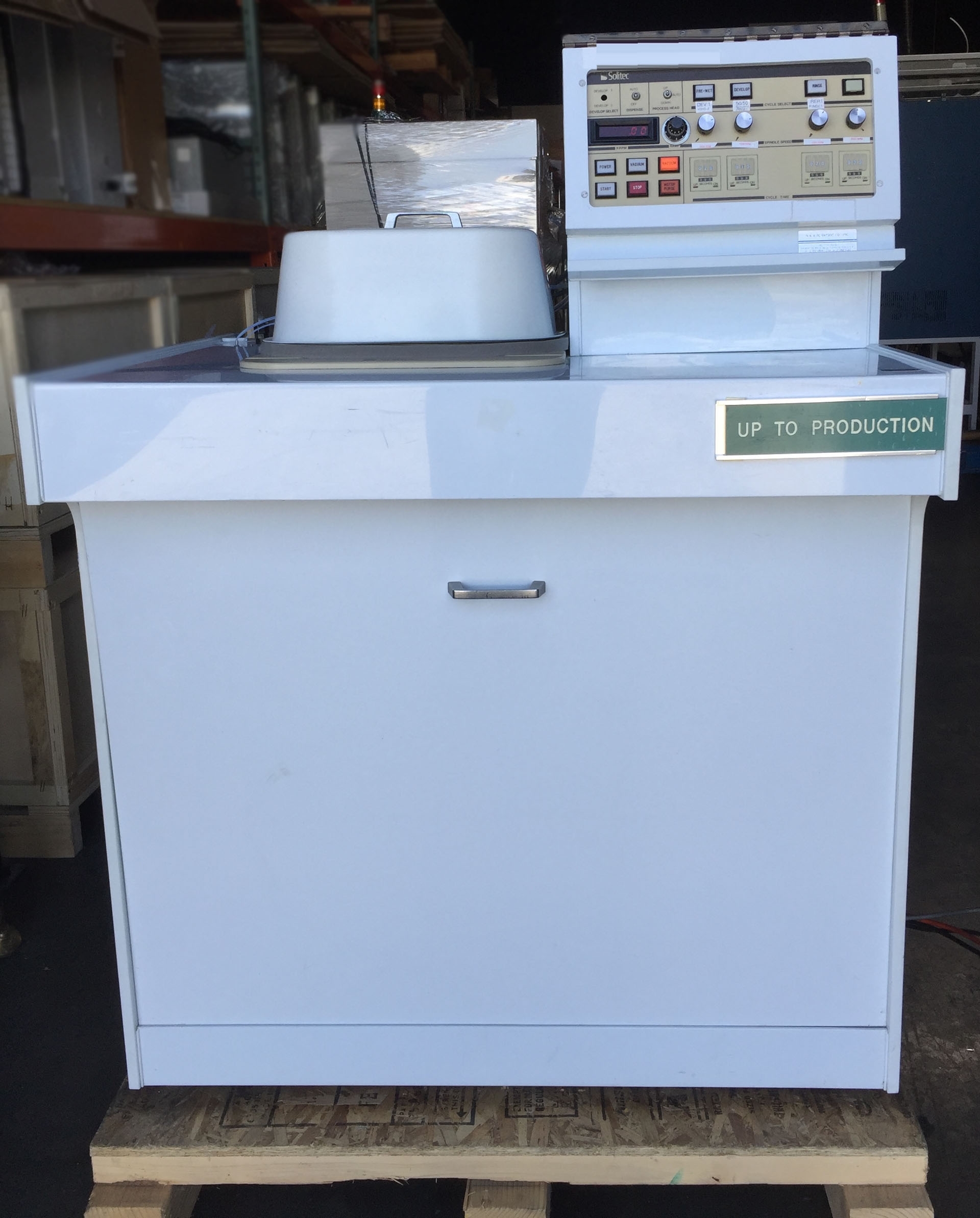


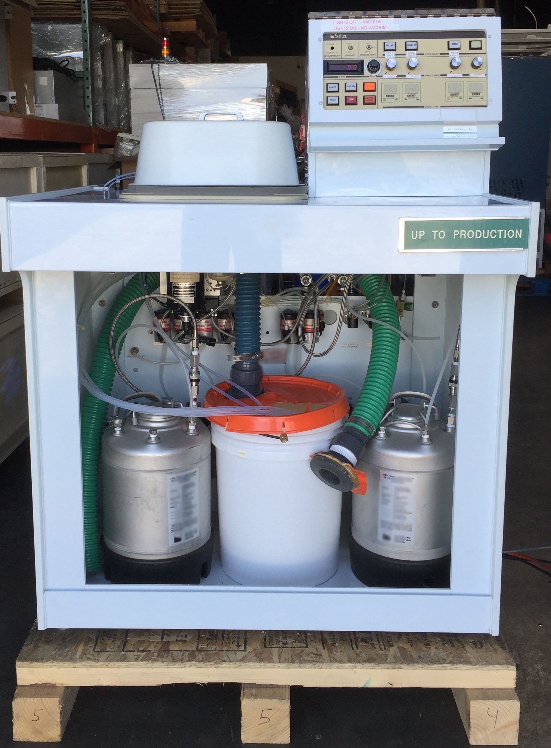


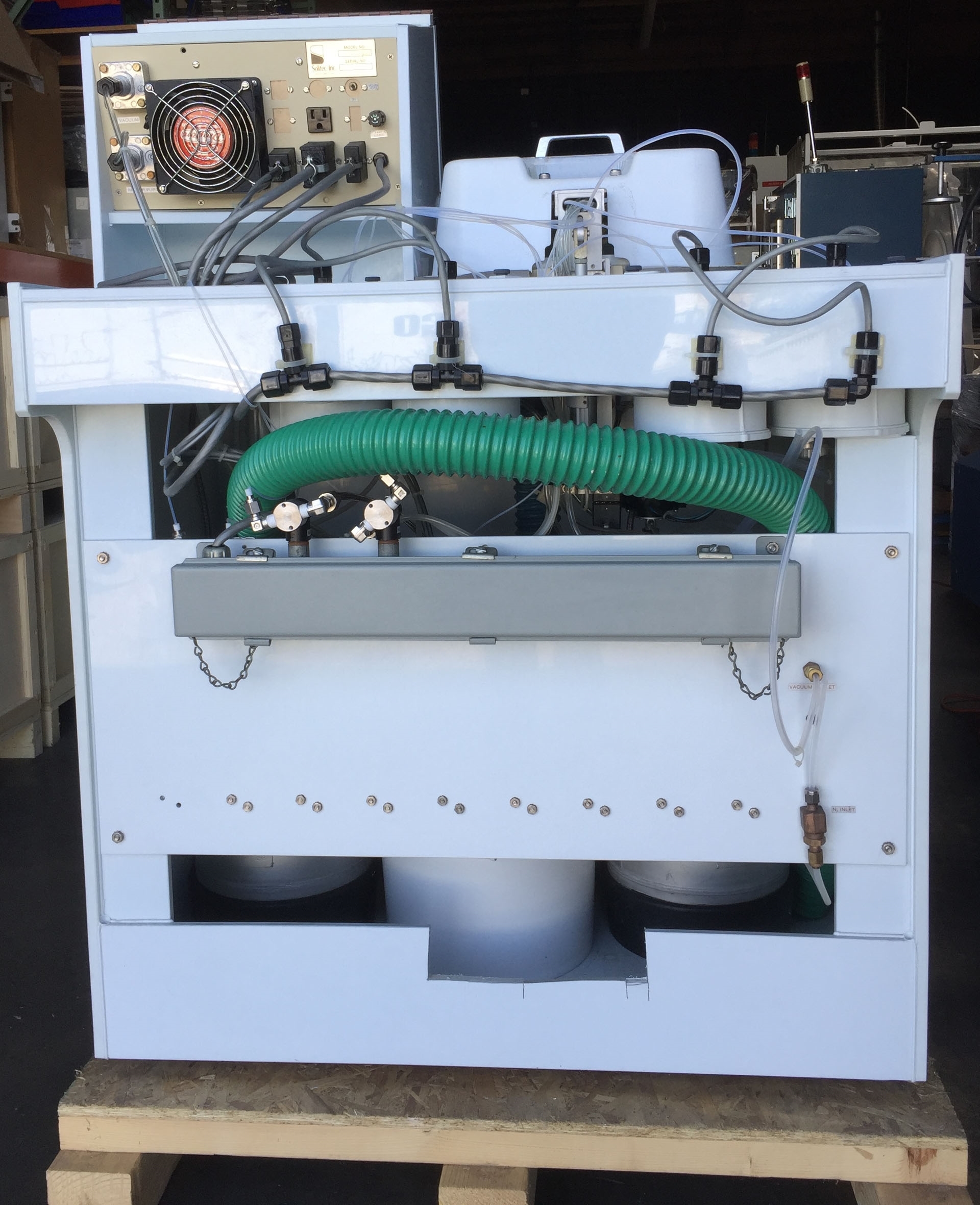





ID: 9270248
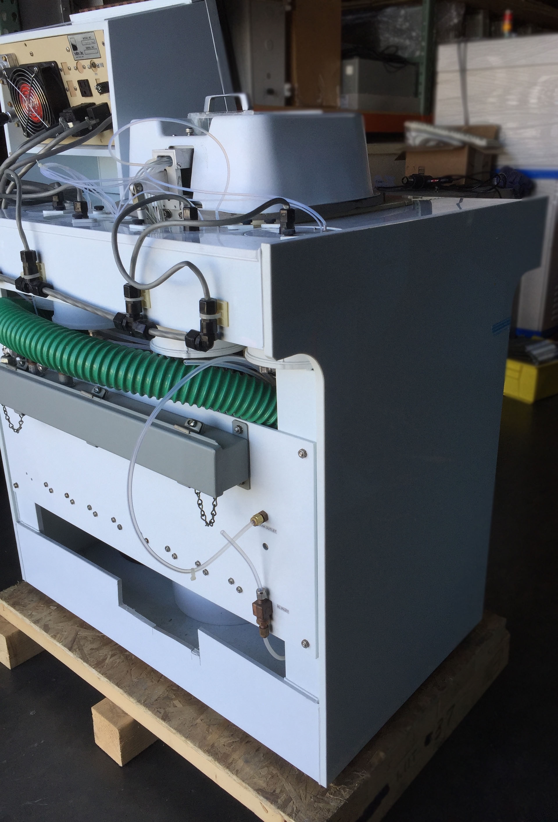
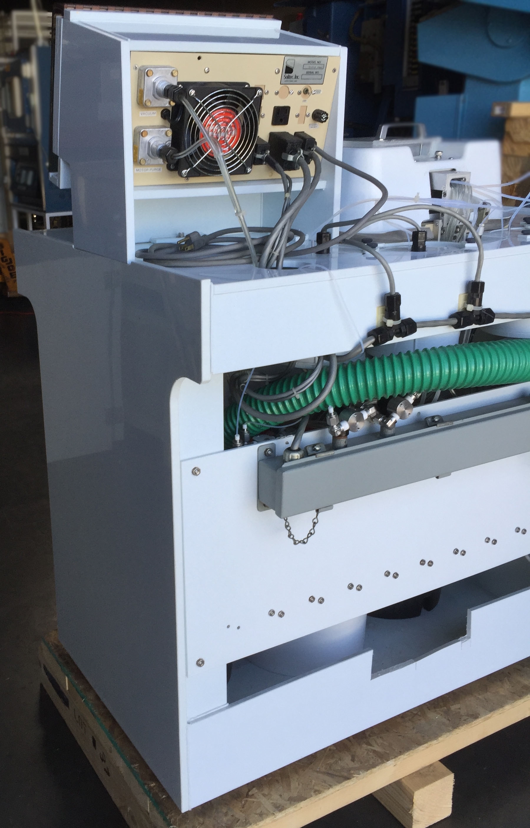
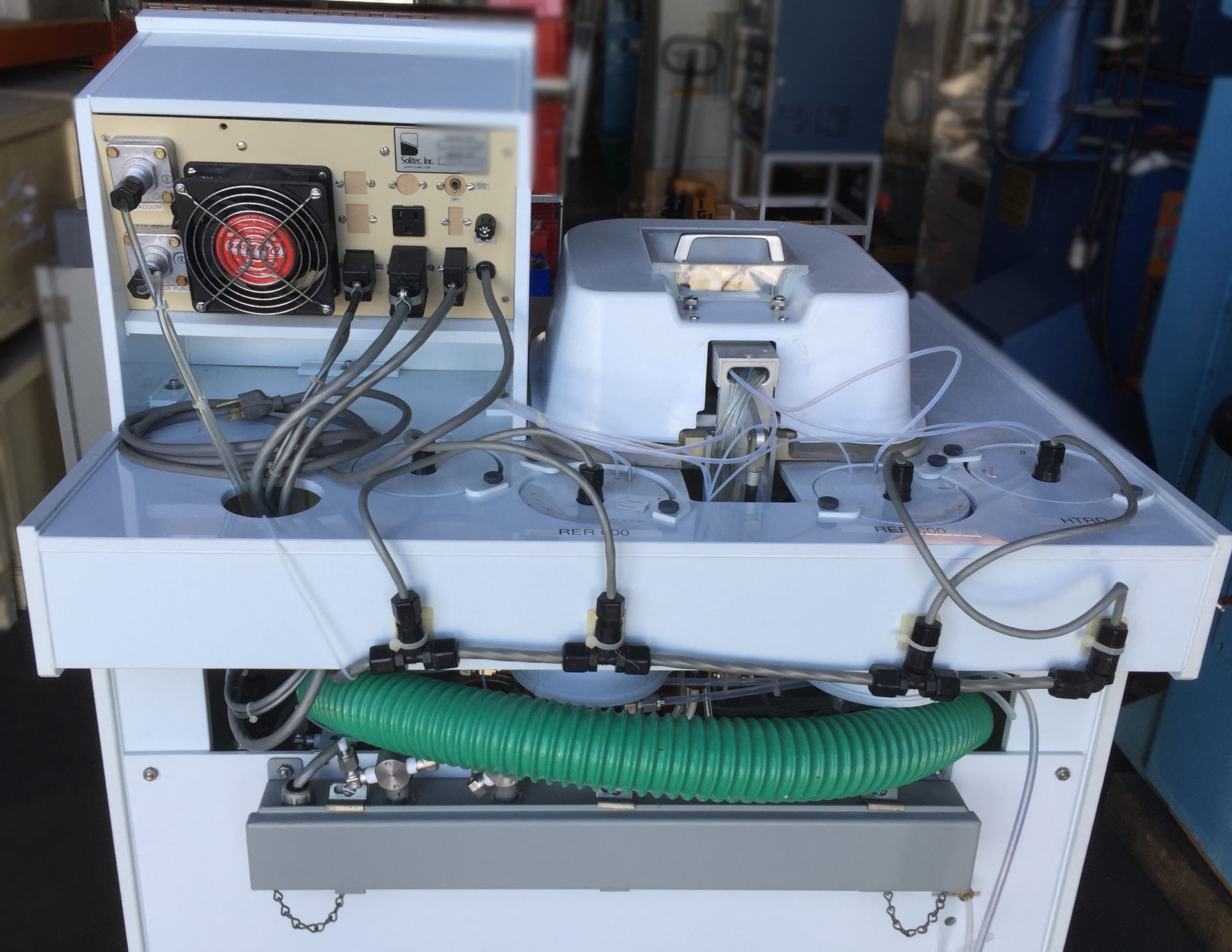
Coater / Developer system
Size: 8 mm
Substrate sizes: 9" Round x 6" Square x 9" Diagonal rectangular
Time: Variable from 1-999 seconds in 1 second increments
Plug-in modules
Acceleration: 1,000-40,000 RPM/s
Spin speed control: ±10 RPM
SOLITEC Diaphragm dispense pump
Single chuck for wafers, masks or substrates
Backsplash control: Downflow exhaust system
N2 Motor purge and interlock
Vacuum interlock on wafer chuck
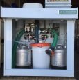
(5) Gallons drain buckets with exhaust
Closed loop servo speed control for tight process control
Polypropylene waste container
Digital tachometer with direct optical encoder
Solvent dispense before coating
N2 Blow-off
Applications:
Positive resist coatings on wafers, masks and substrates
Negative resist coating on wafers, masks and substrates
PMMA and E-Beam resist coating
Silicon, GaAs, InP and other semiconductor materials
Polyimide coatings on wafers, masks and substrates
Photosensitive polyimide coating
Multi-layer resists.
Includes:
Wafer chuck and loading paddle
Operations manual.
SOLITEC 5110-D Photoresist Equipment is a photolithography tool used in the creation of integrated circuits. This system is designed to allow manufacturers to efficiently create nanoscale structures with precision. The unit utilizes a three-channel light source and advanced software to adapt to the complexities of process requirements, including a wide range of doping concentrations and exposure times. Photolithography systems are composed of several parts that are essential to the photoresist processing of substrates. The light source is the first part and is responsible for emitting UV light in three frequency bands, 365 nm, 405 nm, and 436 nm. This light is then collected by a set of lenses and focused using a reticle onto the sample. The reticle is controlled by a computer and is responsible for providing the critical patterning of the substrate. The machine can also be used in concert with an e-beam lithography tool, allowing for further pattern refinement. In addition to the direct patterning capabilities of SOLITEC 5110D, there are additional features that make it ideal for production-level nanoscale structures. An automated sequence of exposure and patterning is possible, eliminating the need for manual adjustment of the light source. Additionally, it has an integrated wafer stepper, which reduces start-up time when working with multiple substrates. For safety, the tool also includes an emergency shut-off switch. To control the patterning process, sophisticated software can be used to manipulate numerous parameters, including exposure time, intensity, duty cycle, etc. This software is based on a classic production-level algorithm allowing for precise control over the entire photoresist process. Additionally, the software can be calibrated to precisely locates the resist layer on the substrate, reducing wasted resources due to wafer misalignment. Overall, 5110-D is an invaluable tool in the production of micro and nanoscale structures. It's adjustable three-channel light source and integrated wafer stepper make it well suited for production-level nanofabrication. The included accident cut-off switch provides safety for users. Additionally, the sophisticated software solves many of the complications of patterning, reducing the need for manual adjustment of the light source. This, combined with its precise patterning capabilities, make it an ideal choice for producing high-quality nanostructures.
There are no reviews yet

