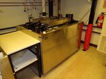
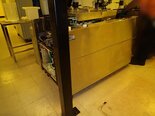
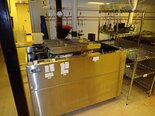
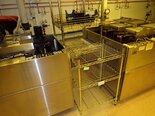
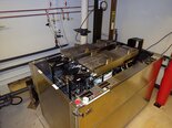
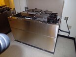
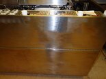
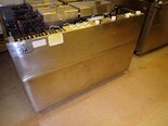
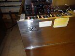
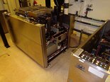
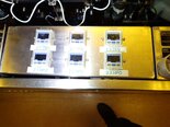
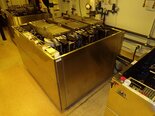
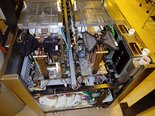
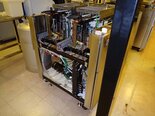
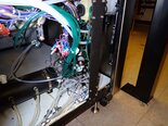
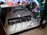
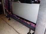
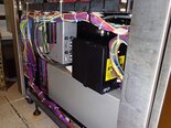
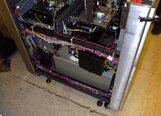
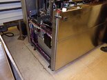
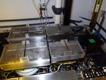
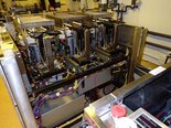
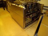
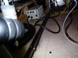
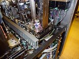
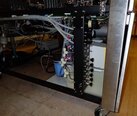
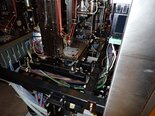
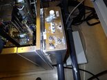
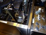
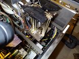
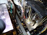
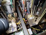
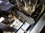
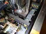
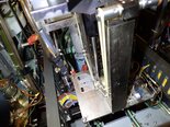
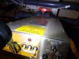
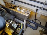
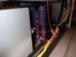
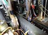
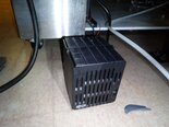
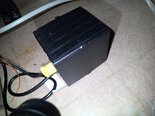
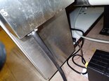
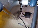
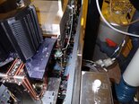
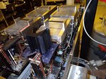
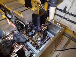
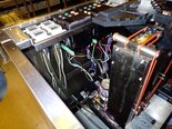
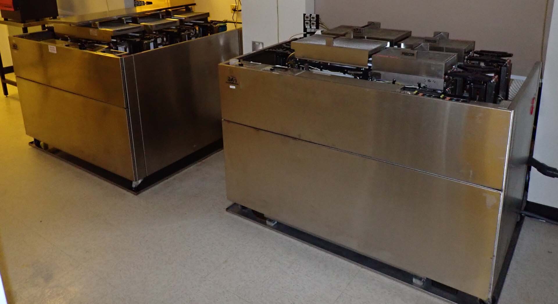
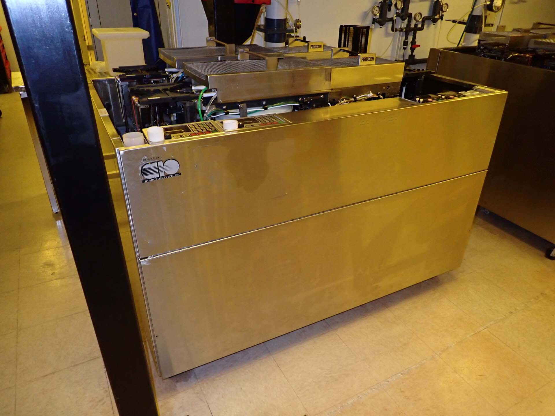
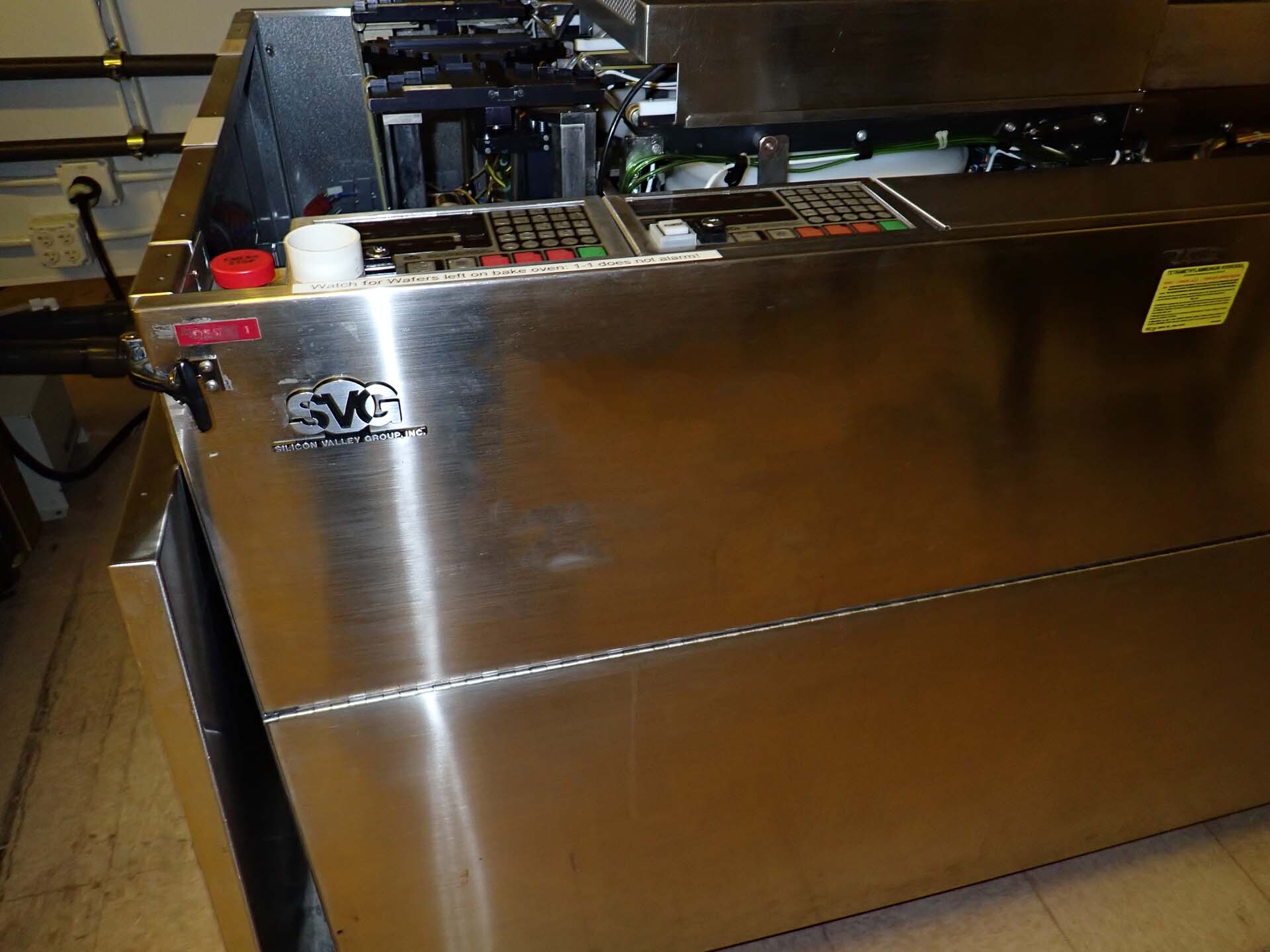
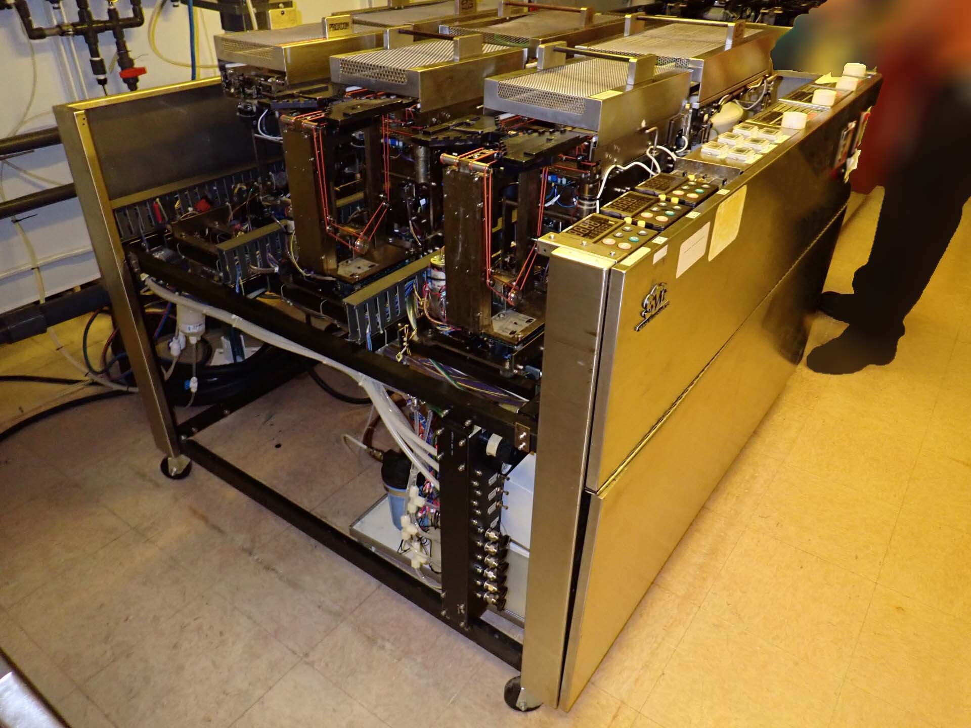
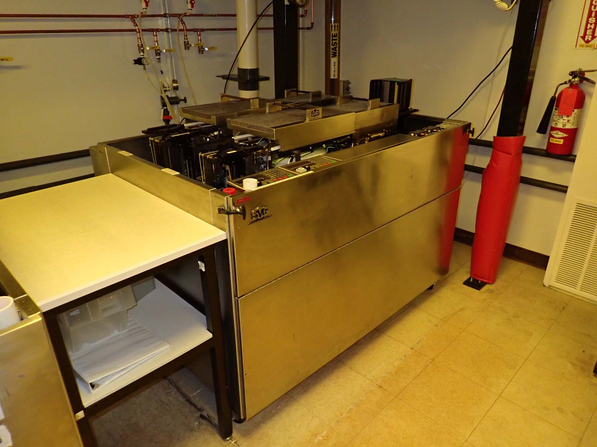
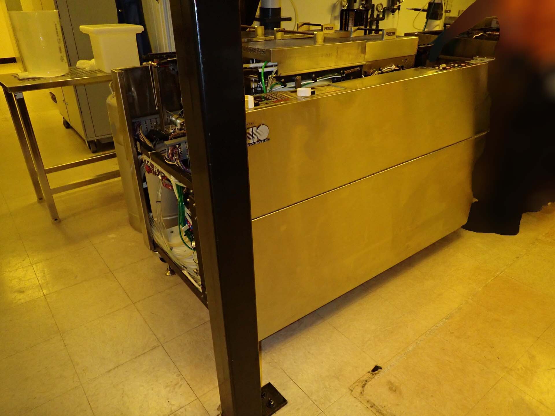
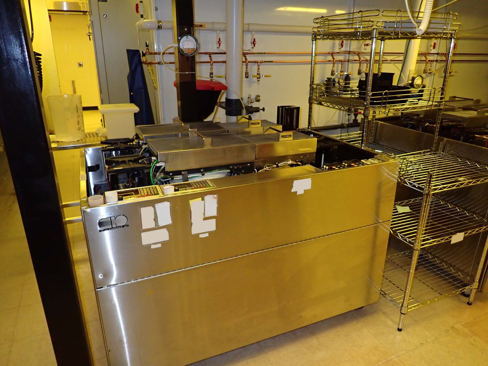
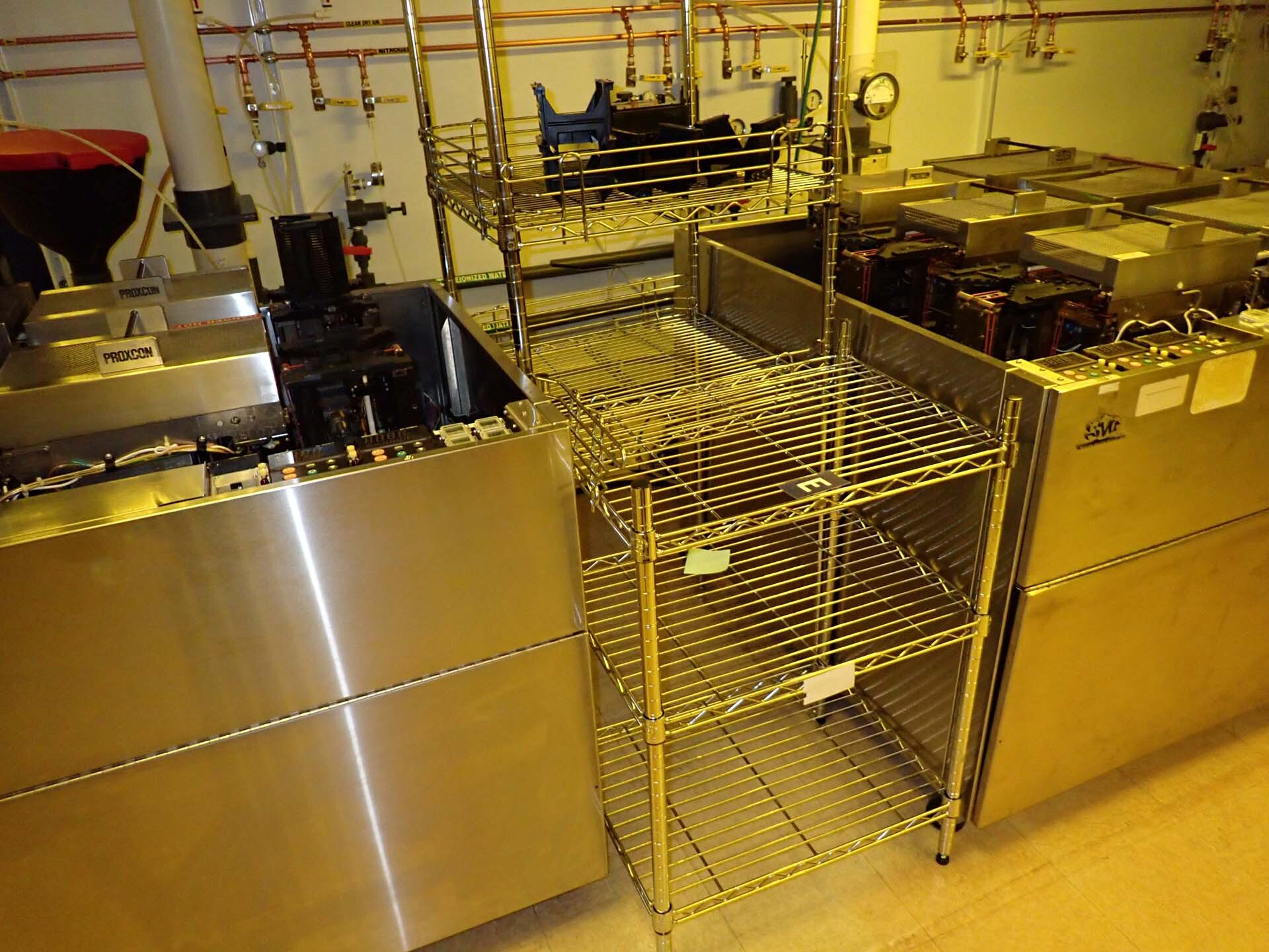
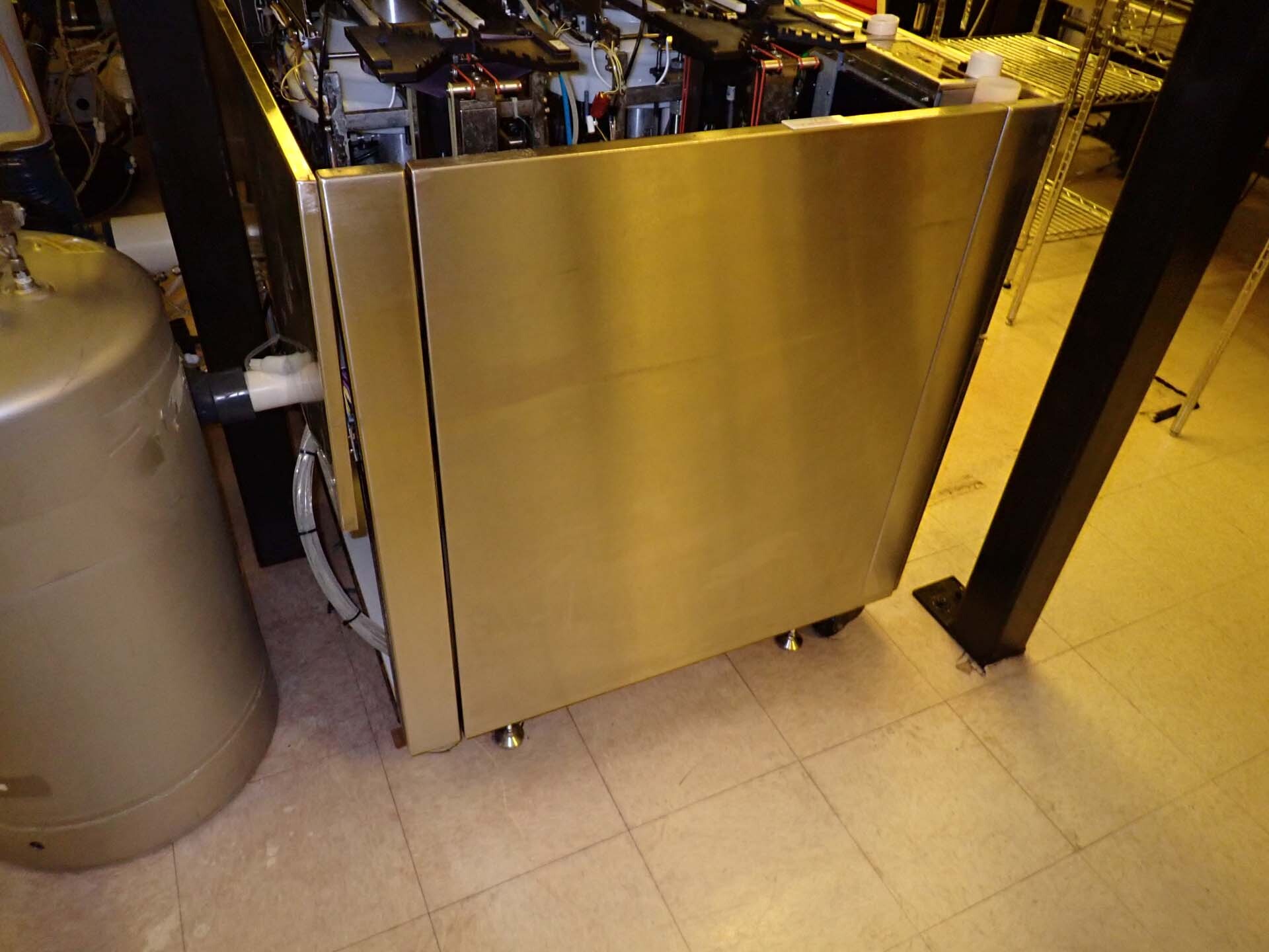
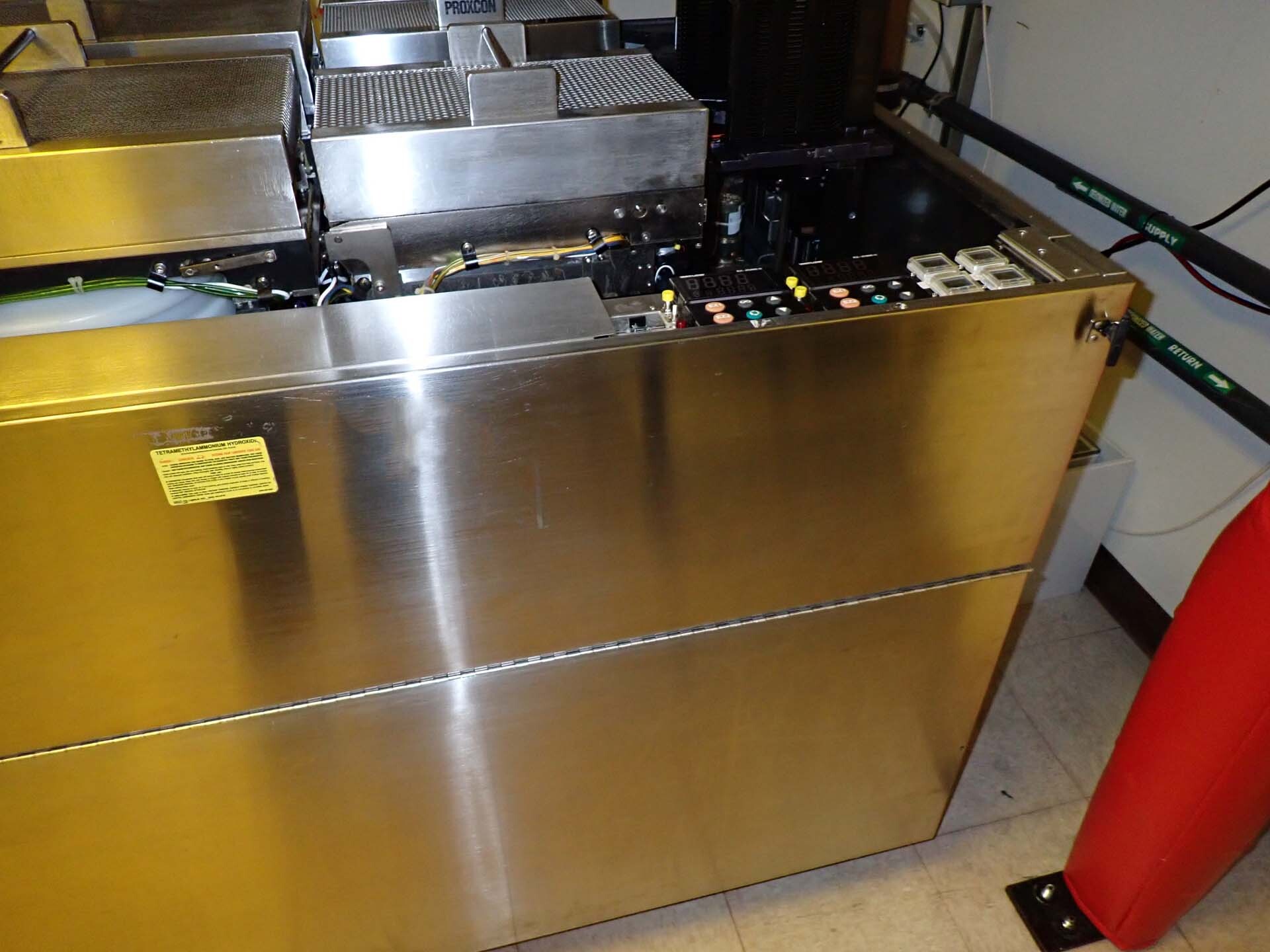
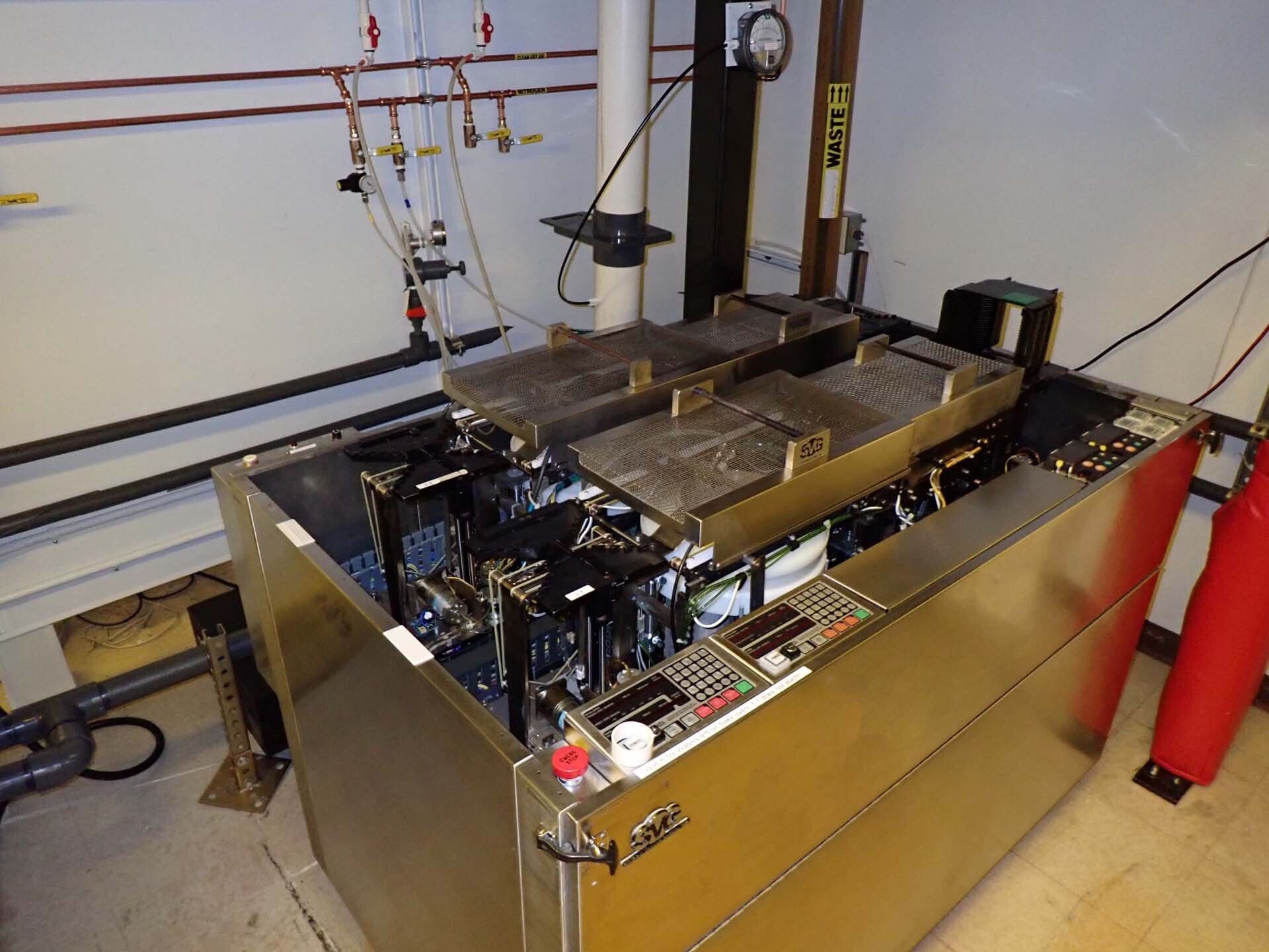
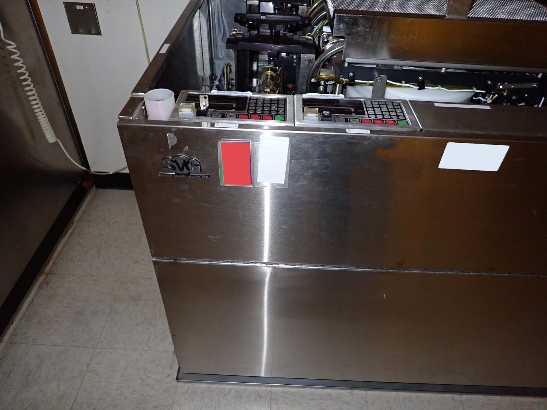
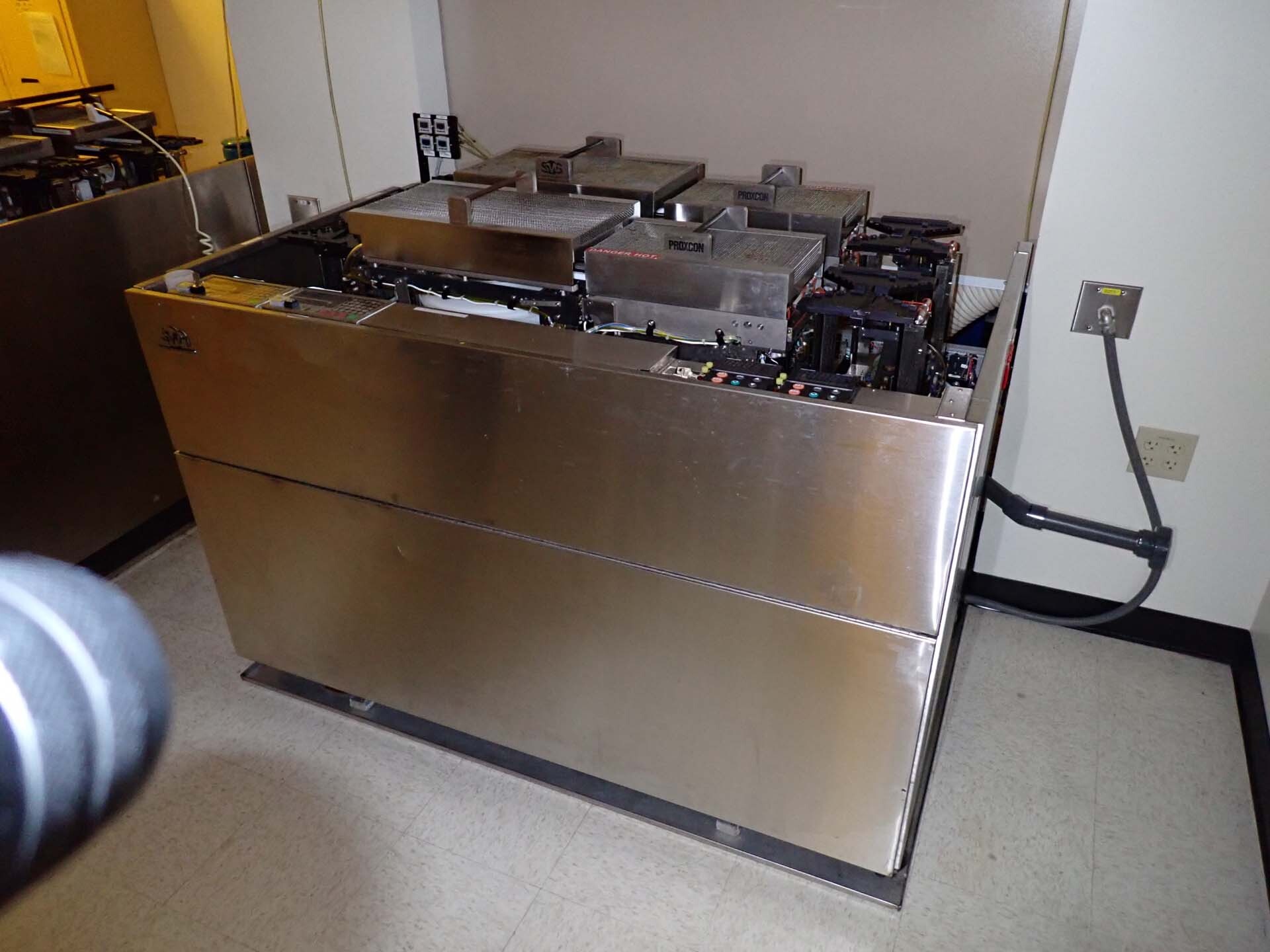
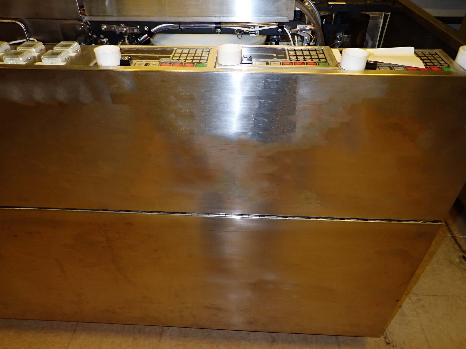
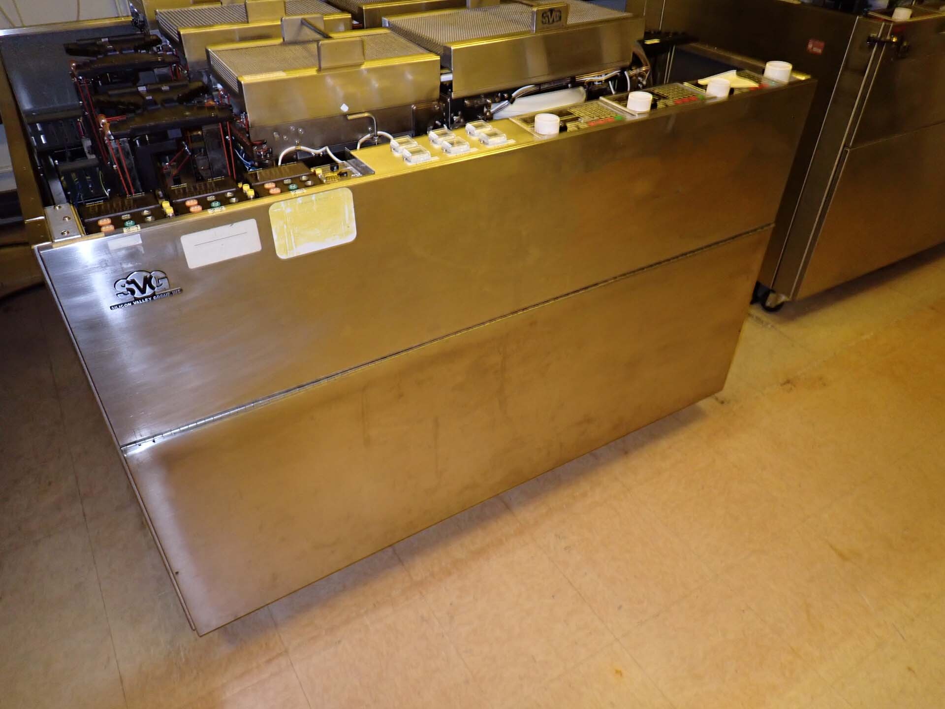
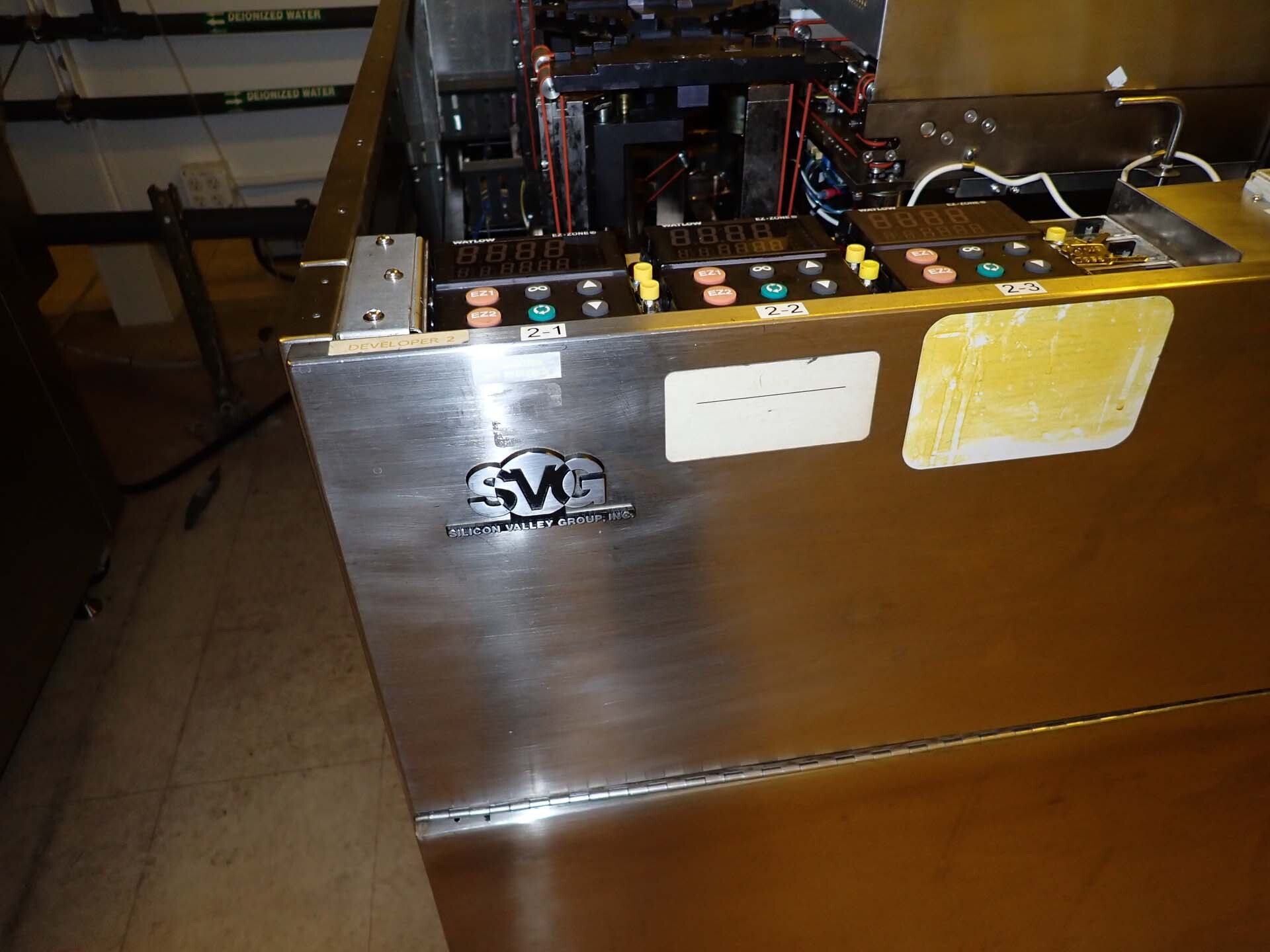
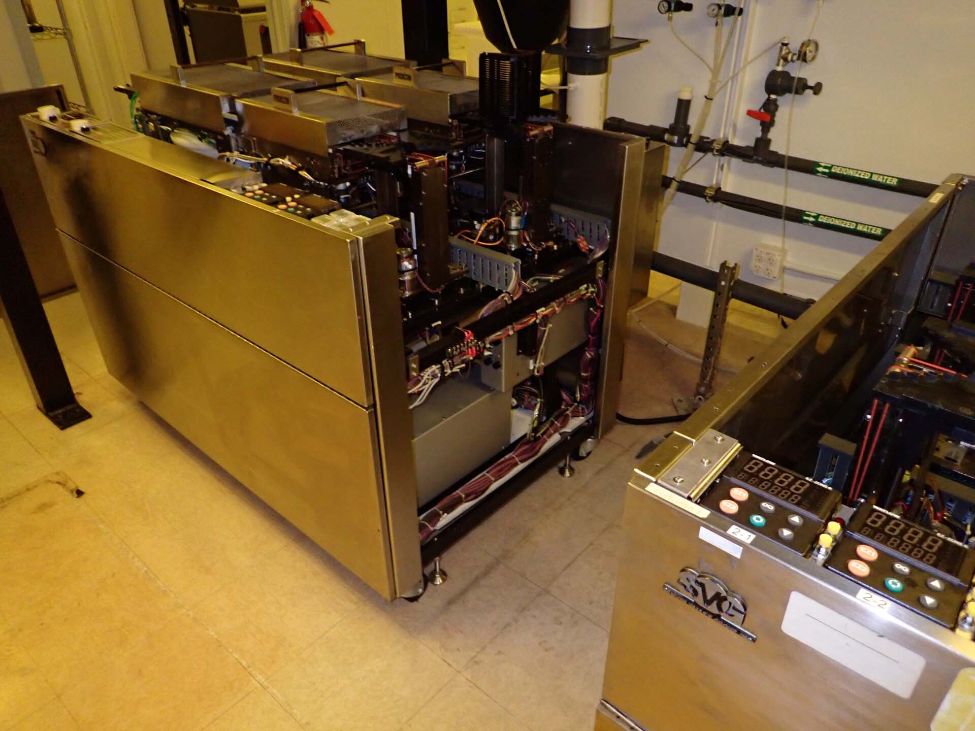
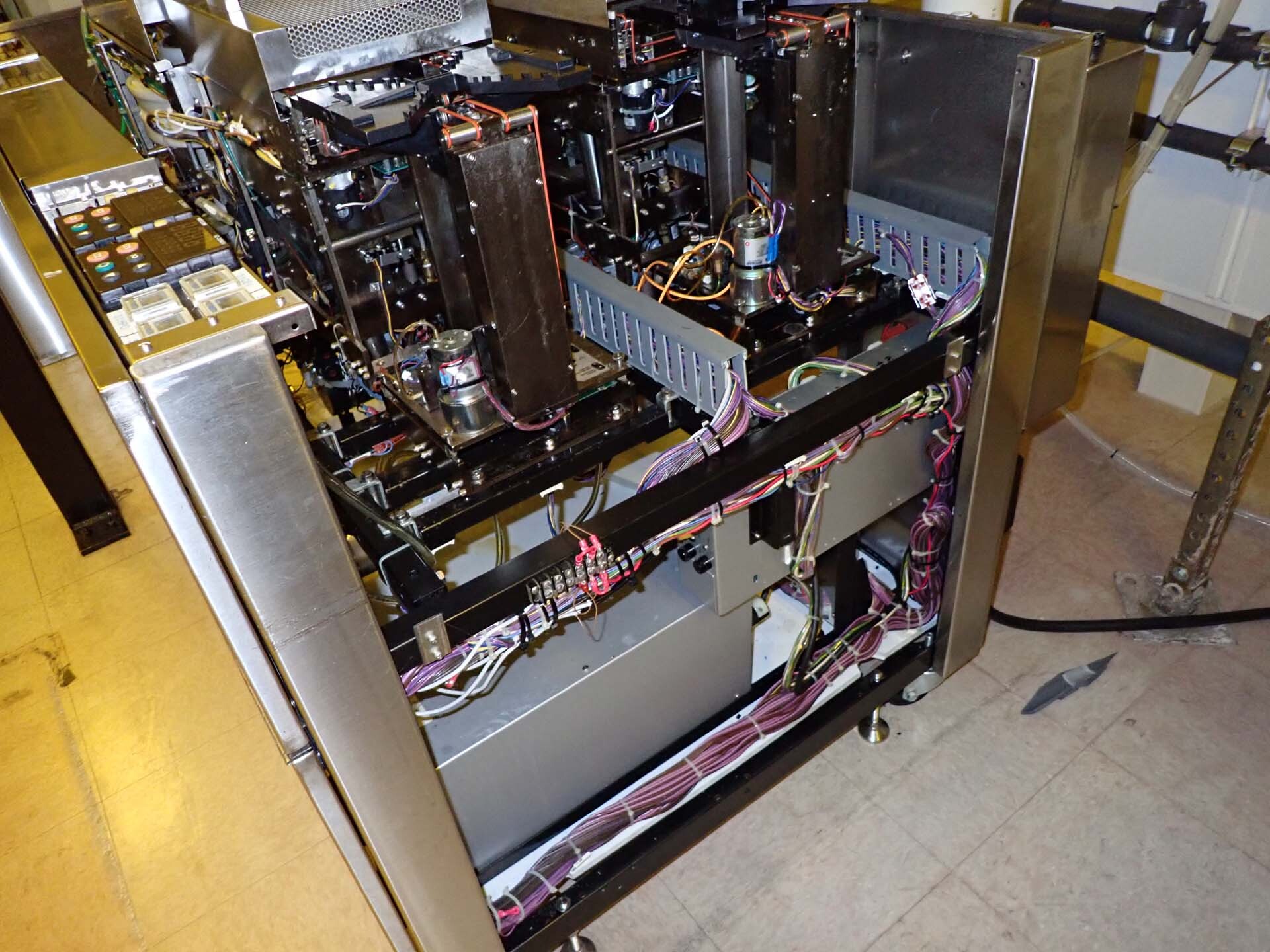
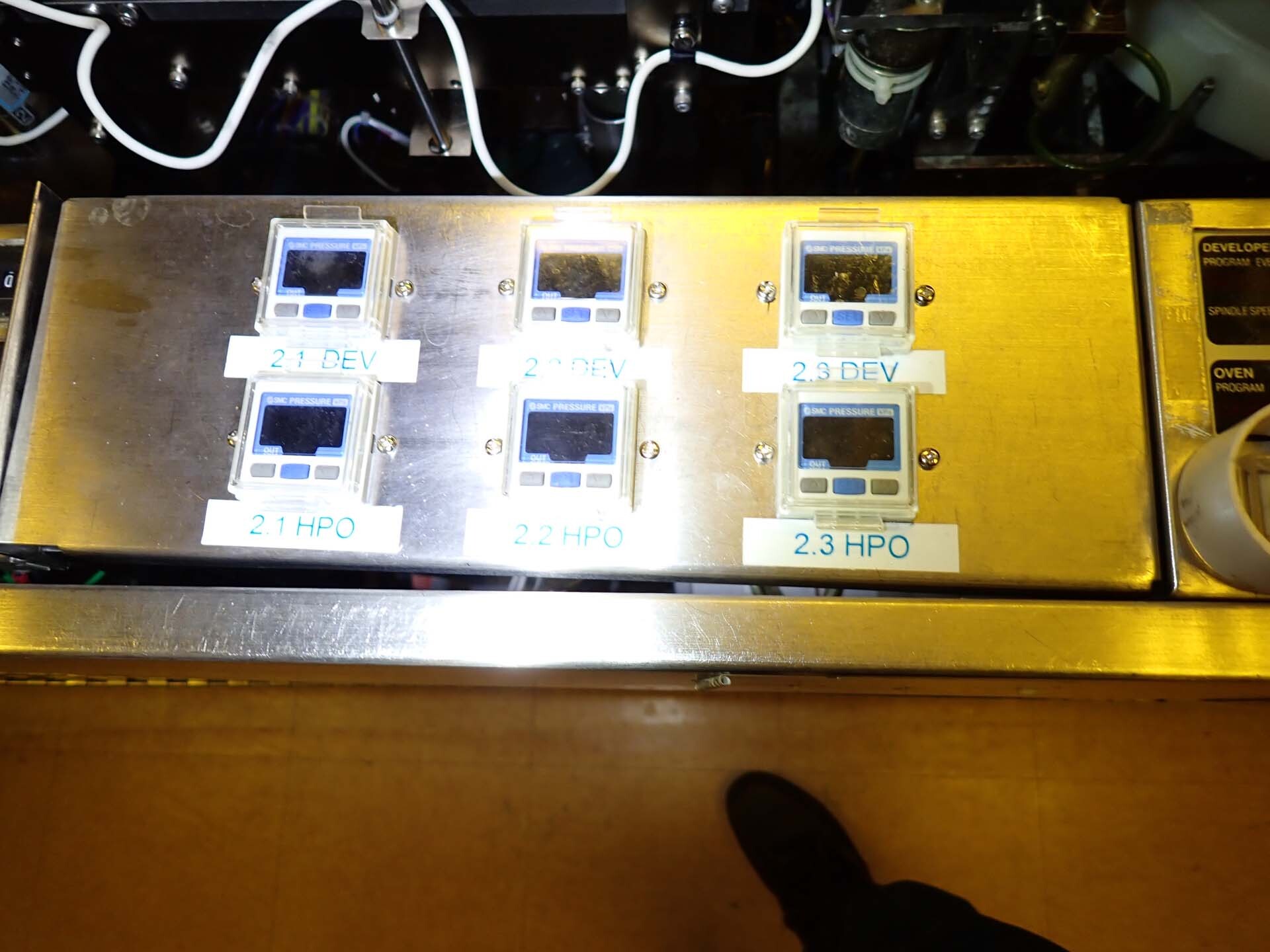
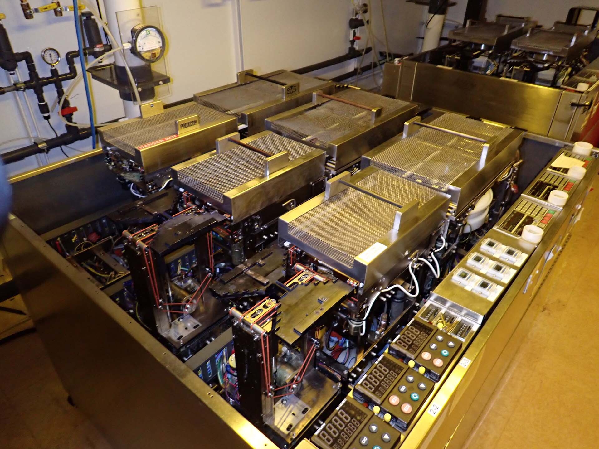
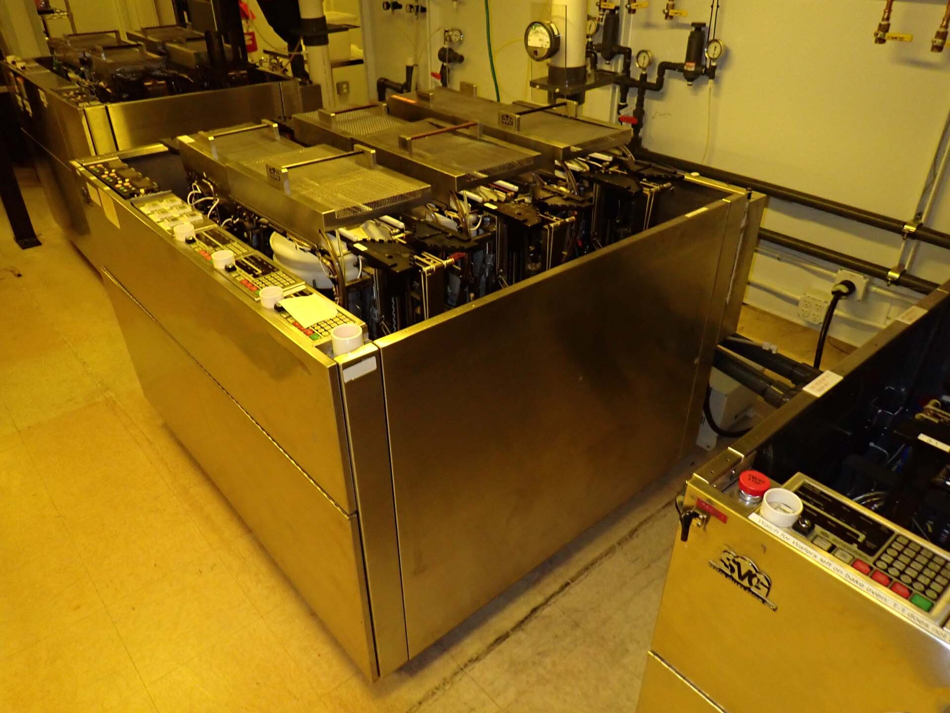
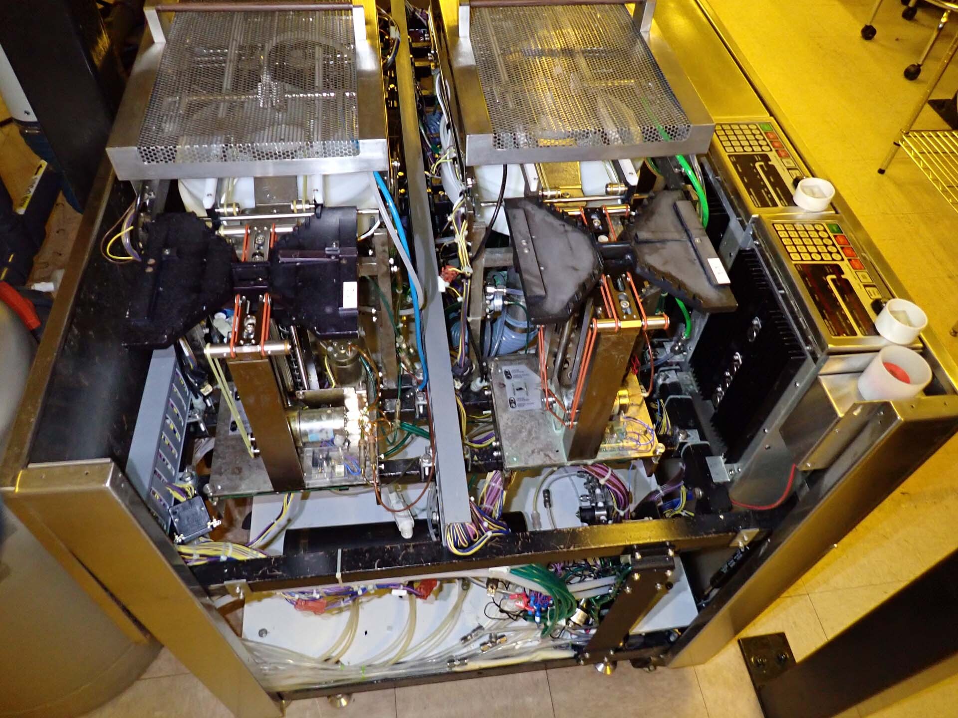
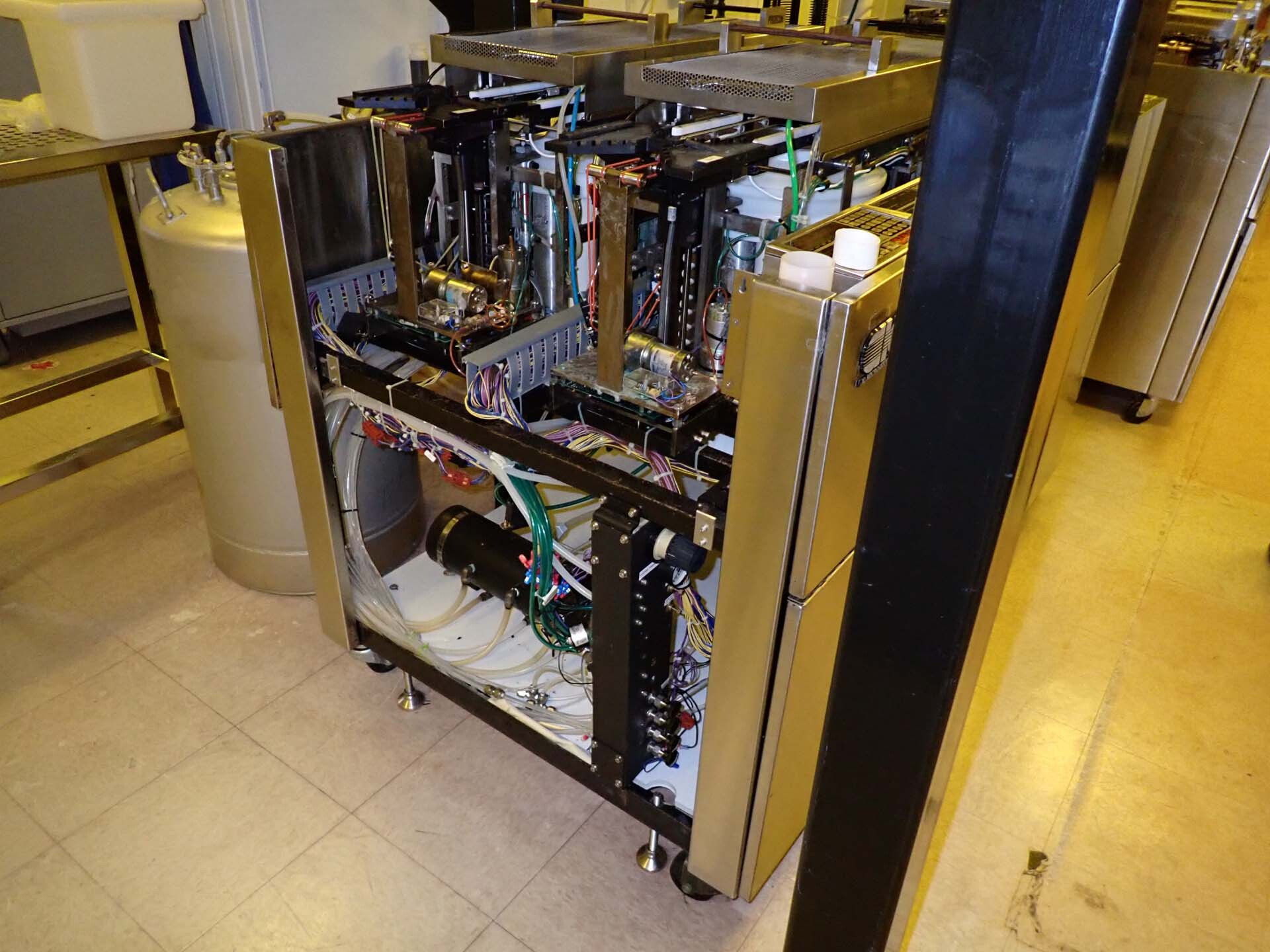
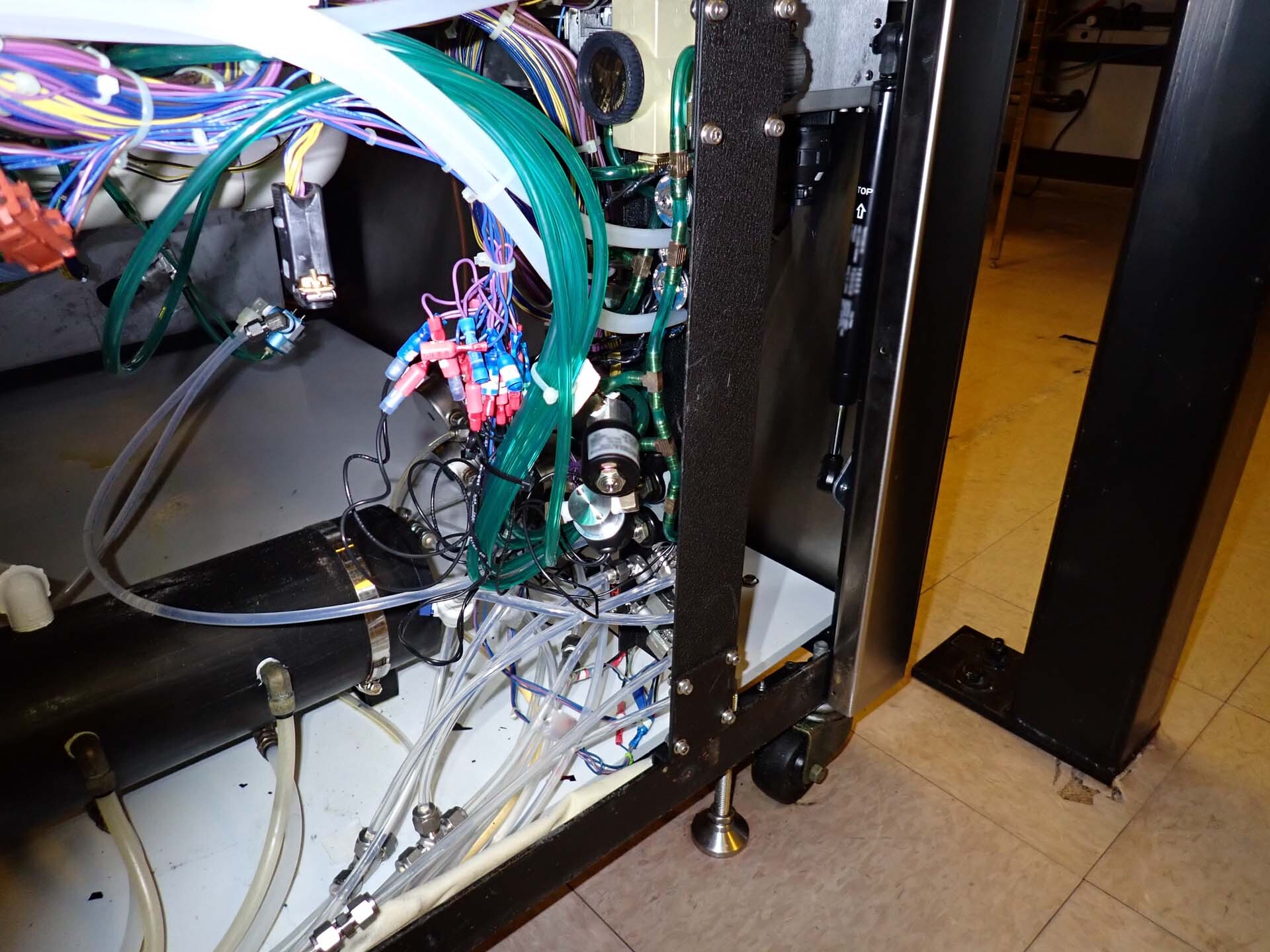
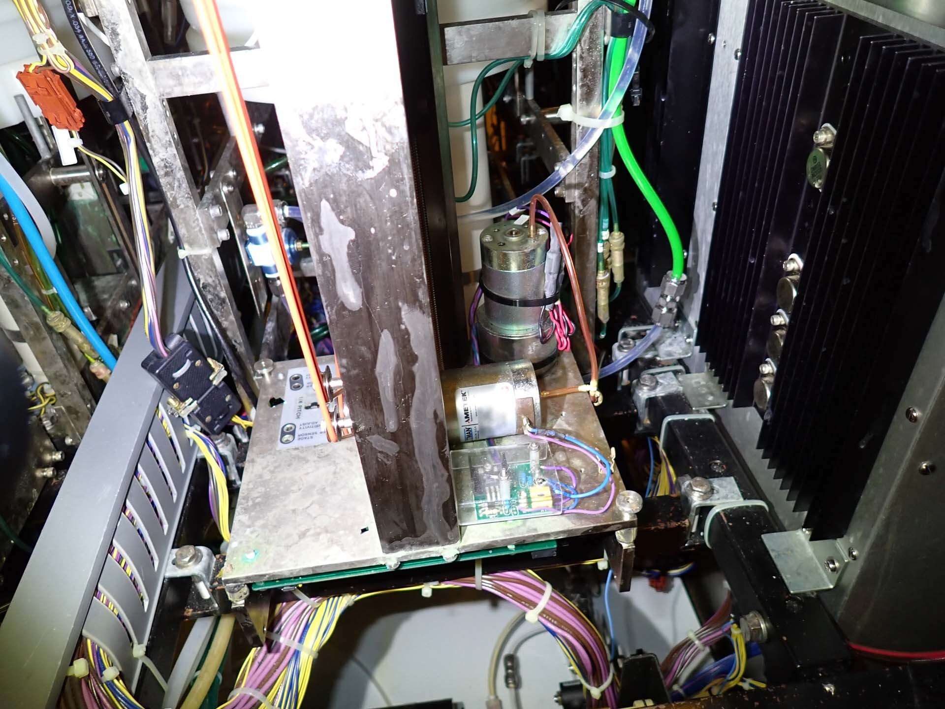
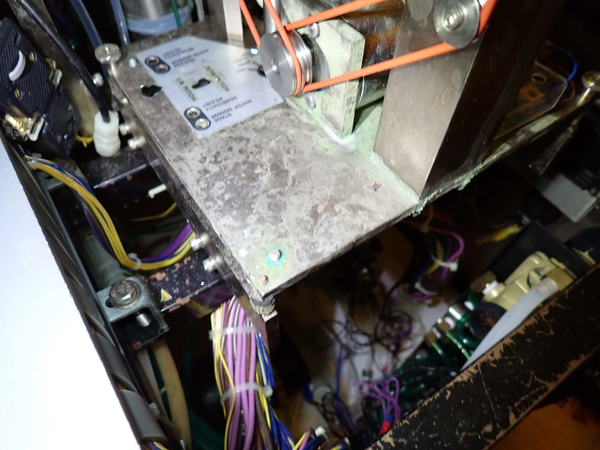
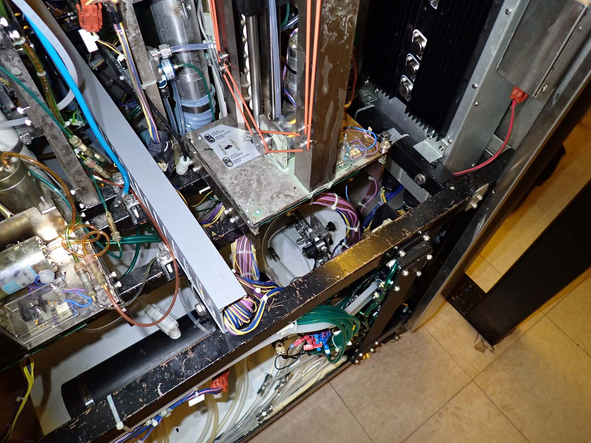
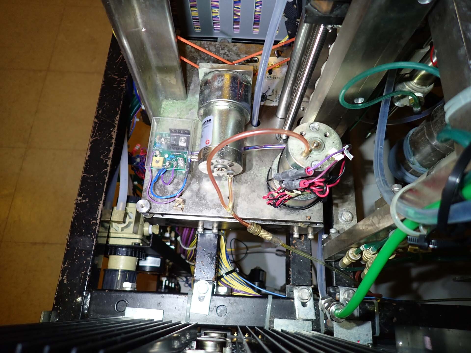
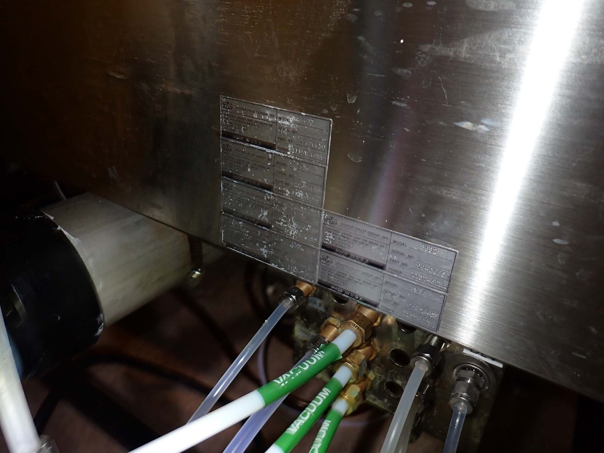
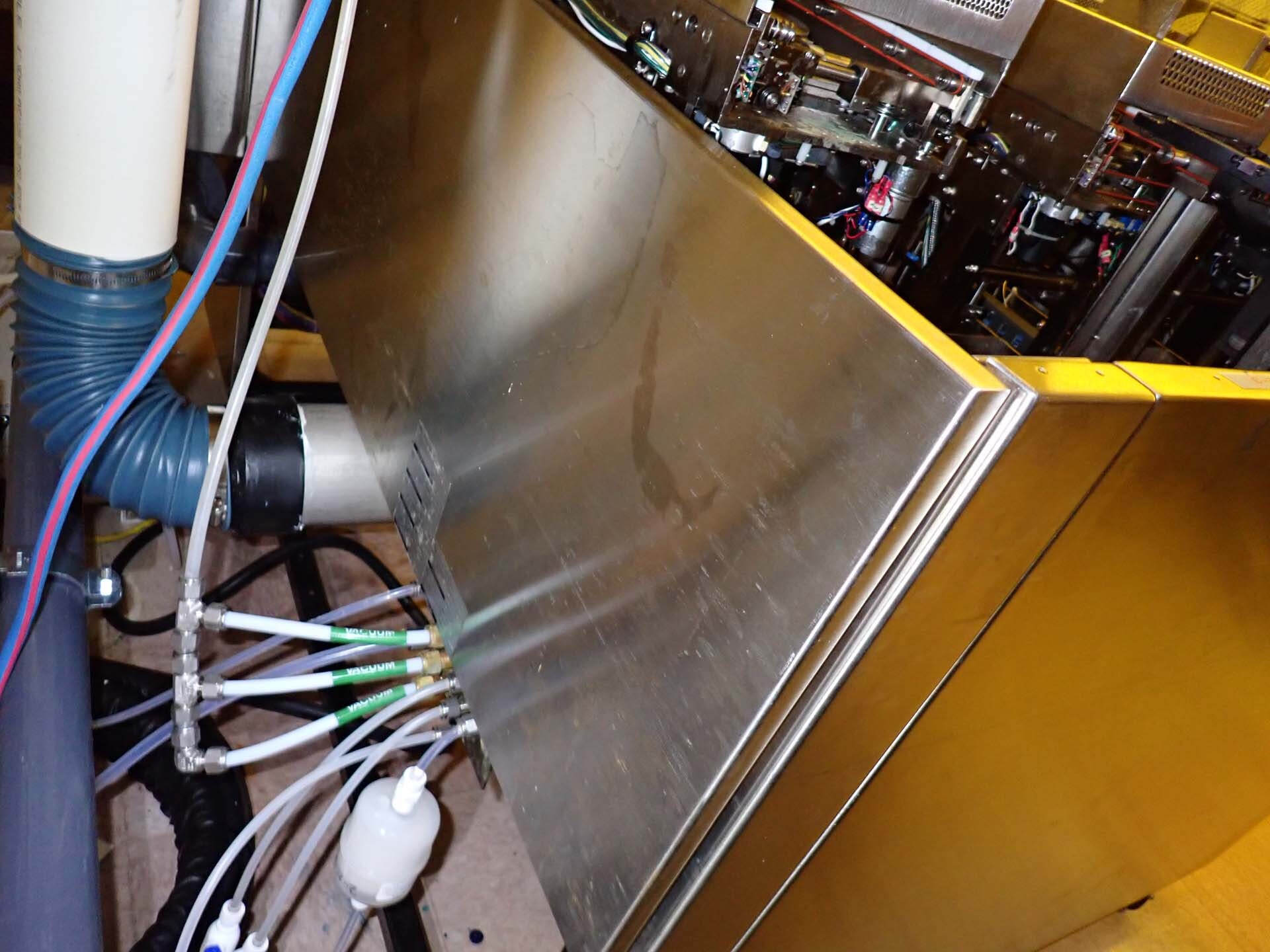
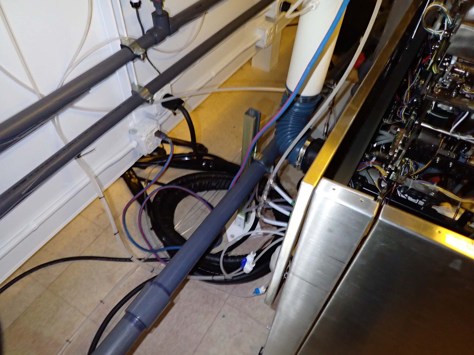
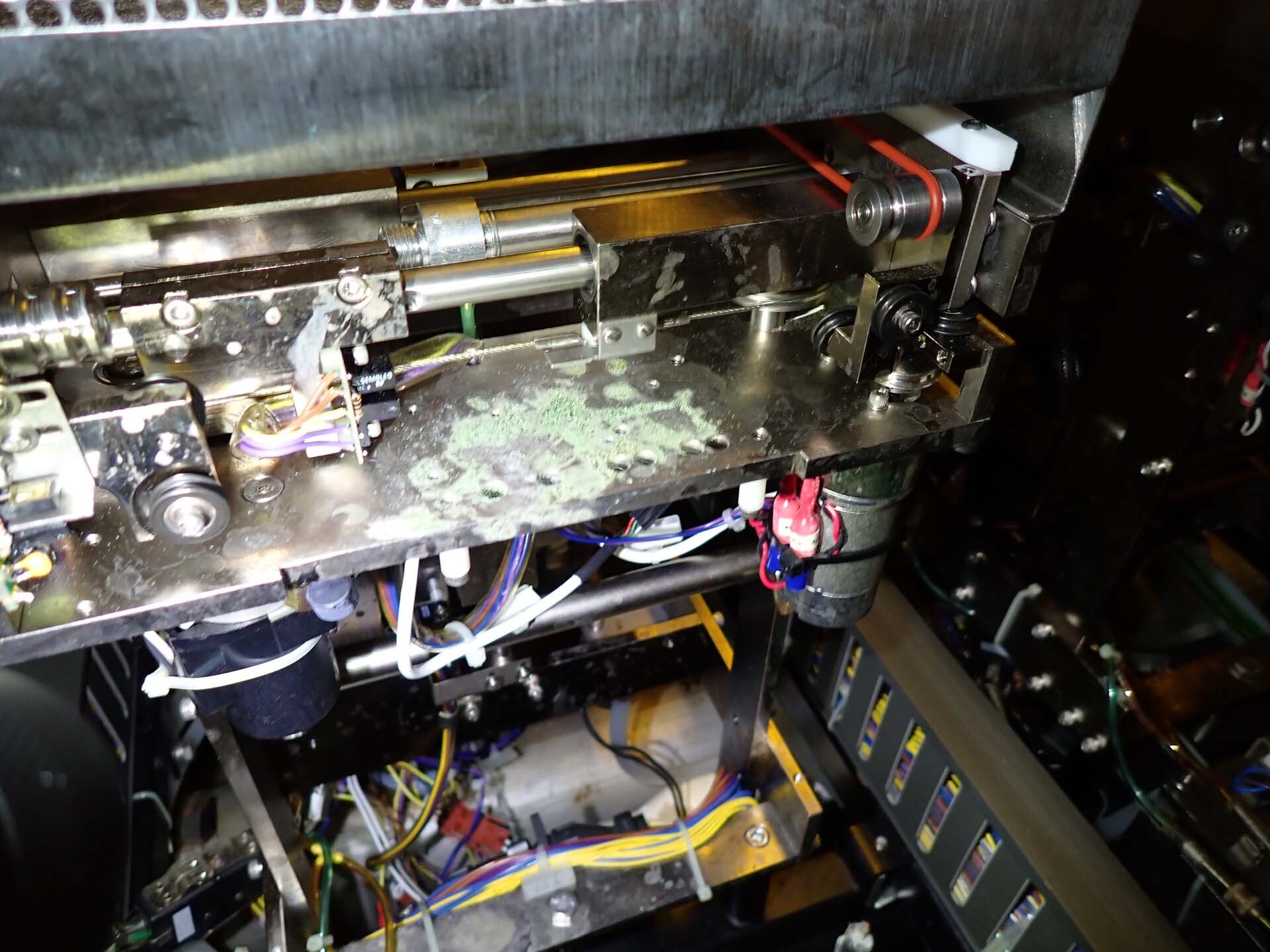
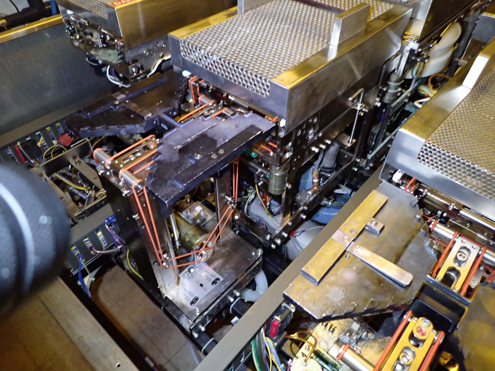
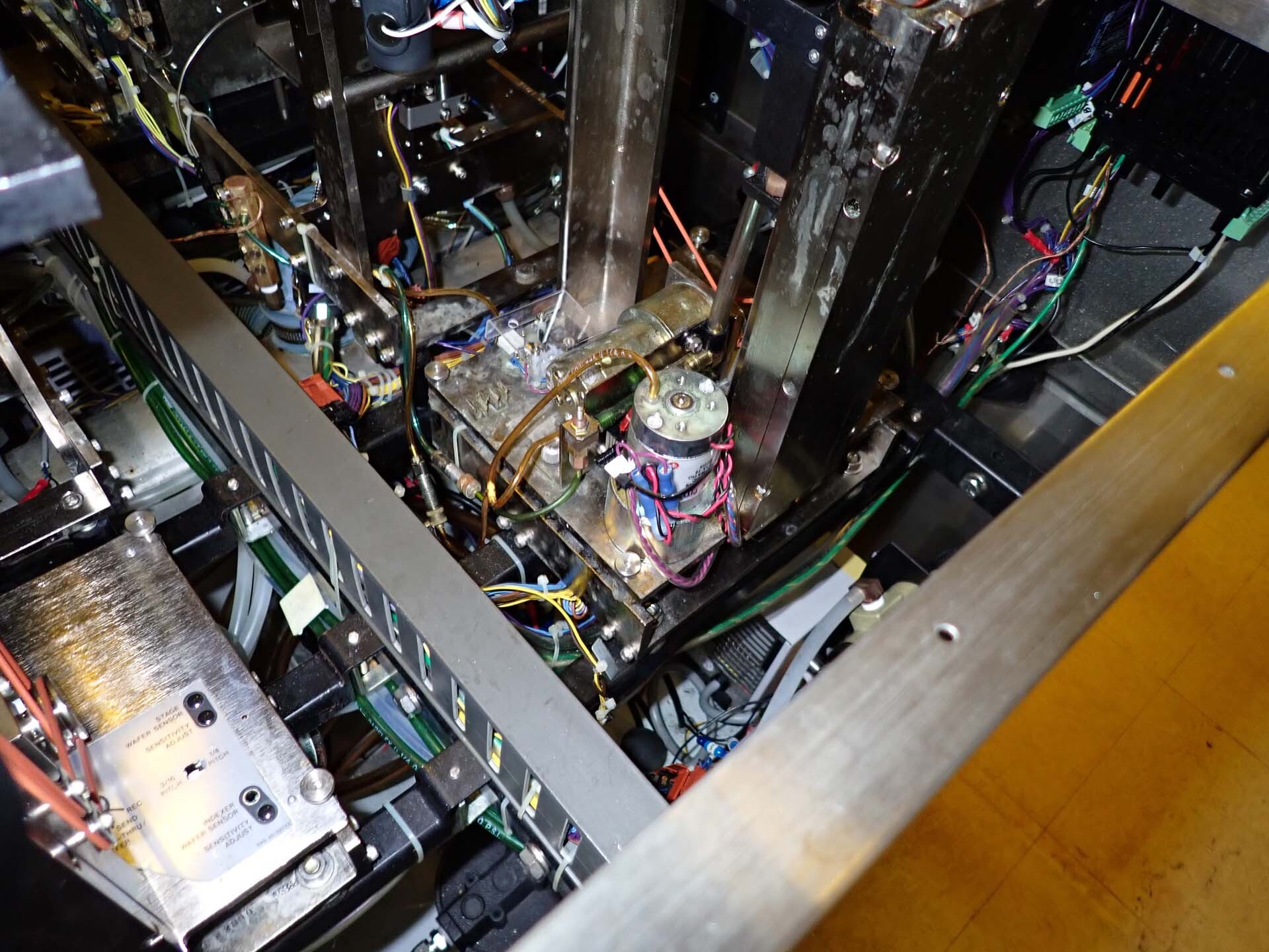
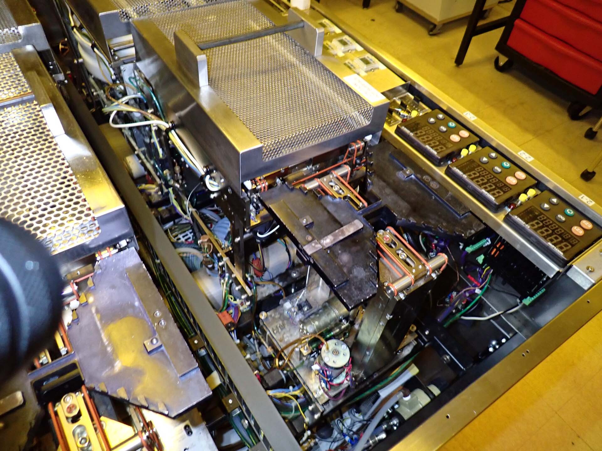
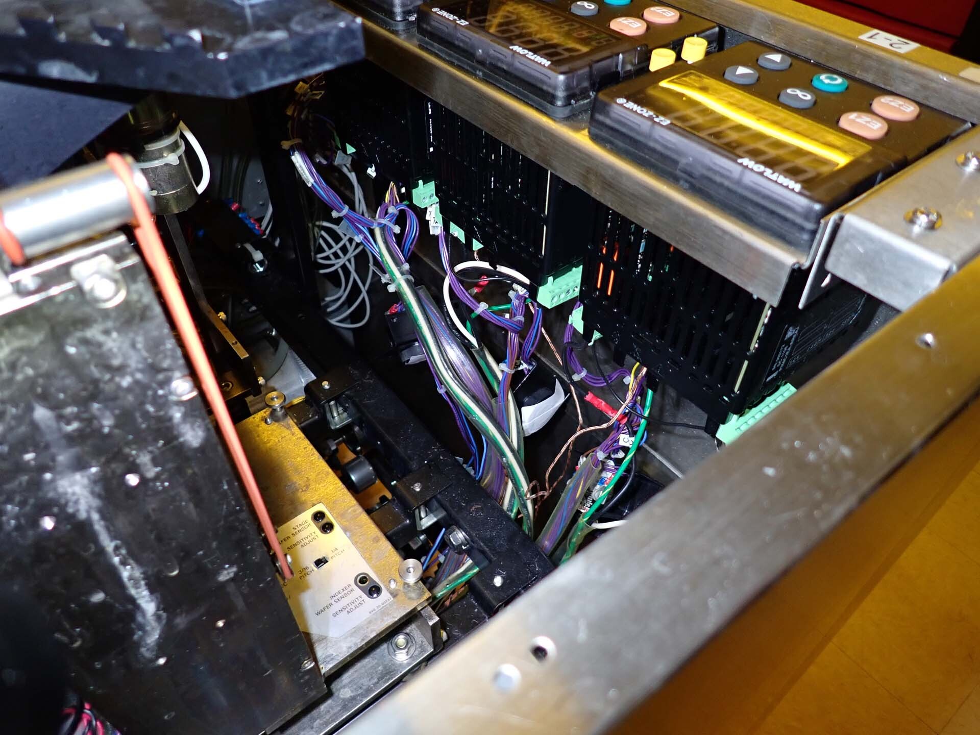
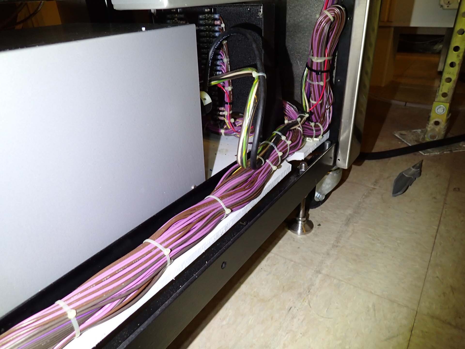
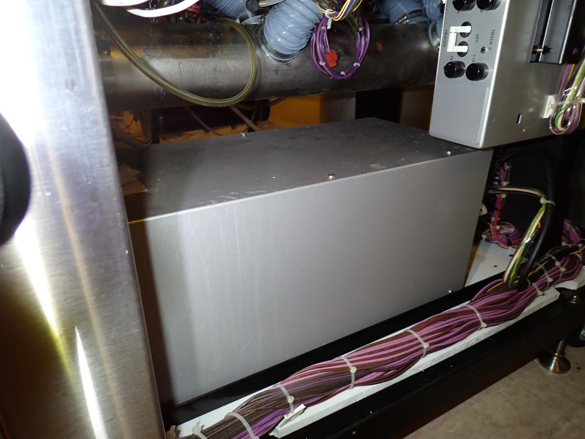
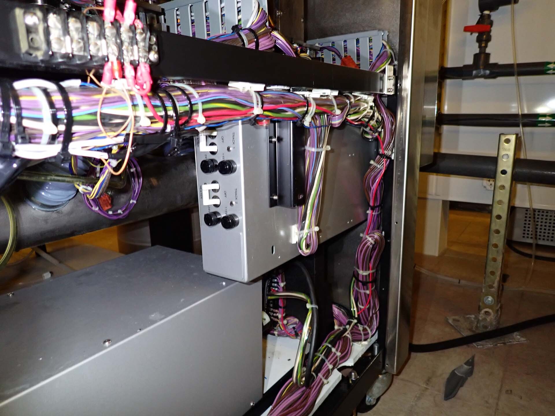
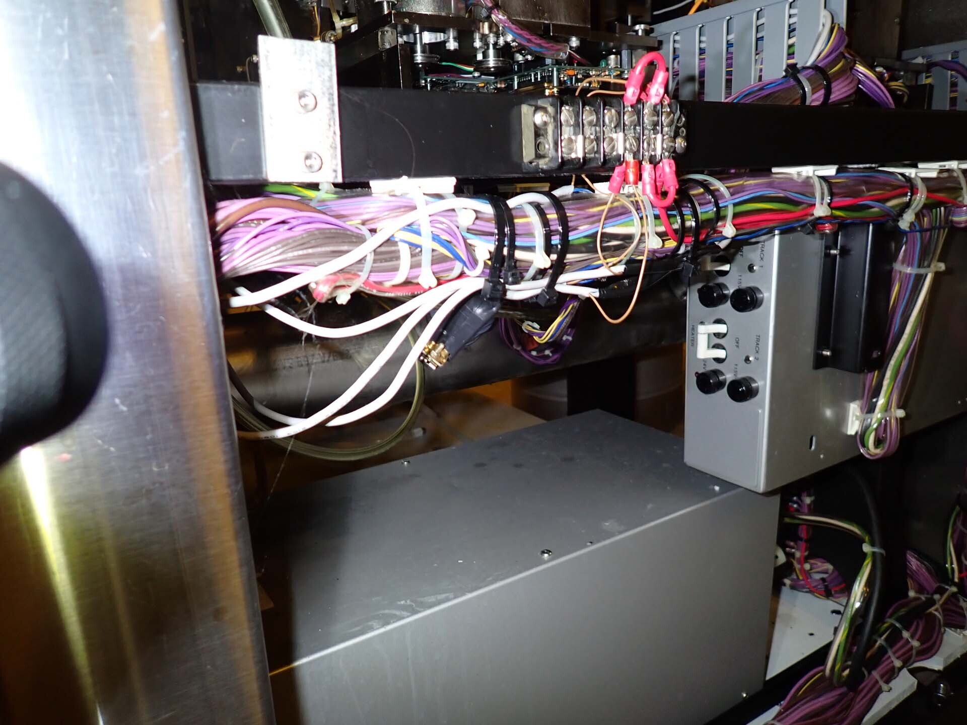
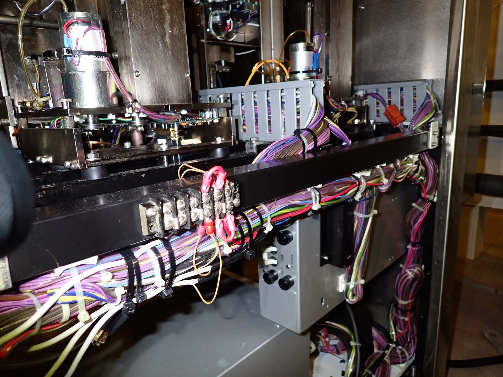
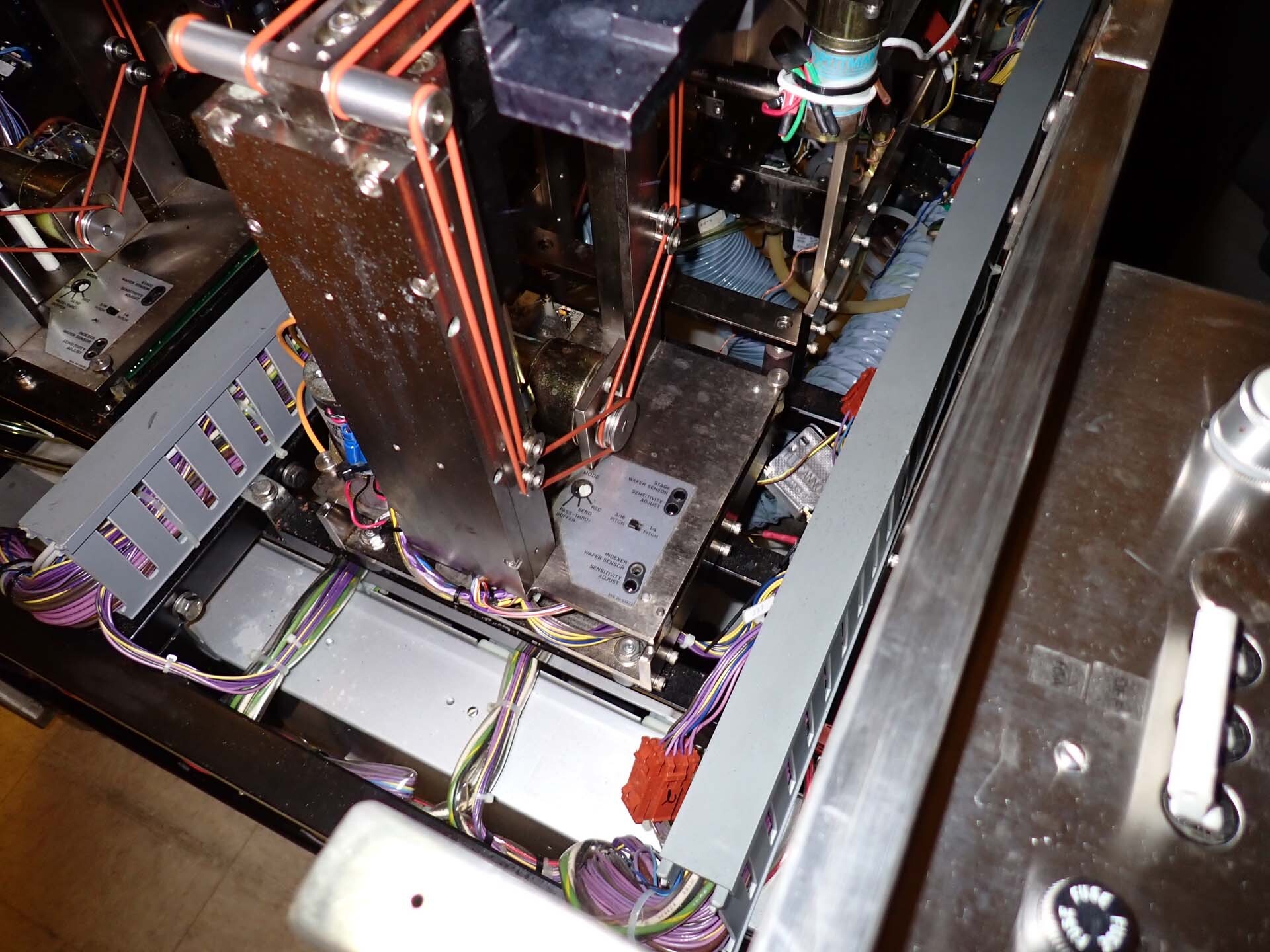
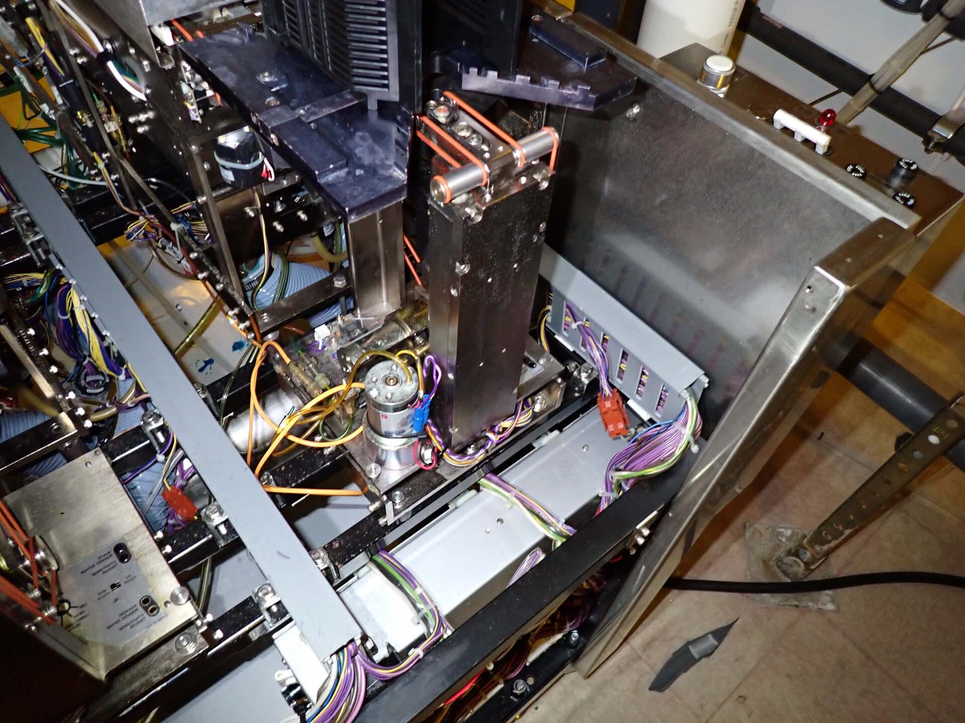
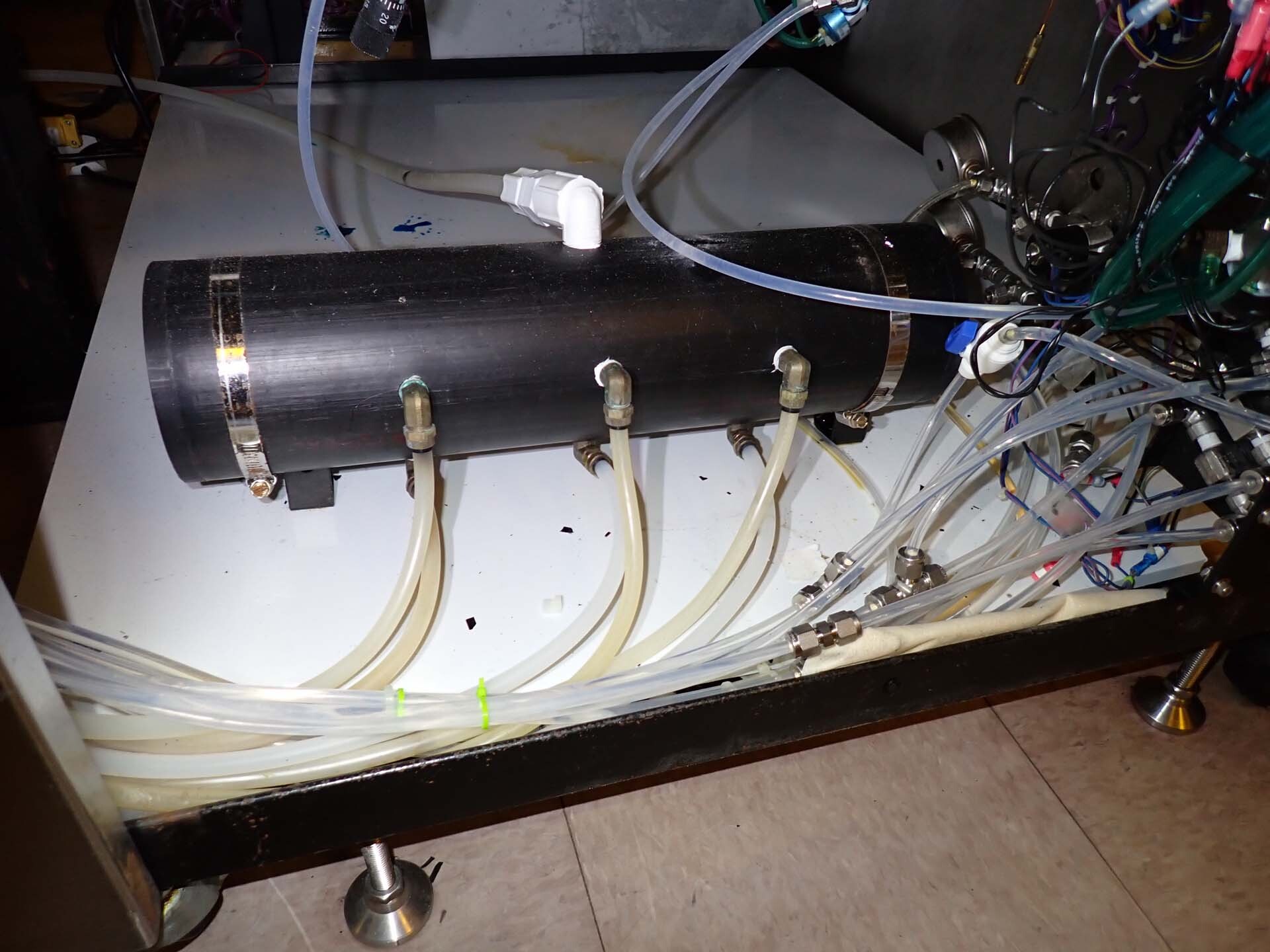
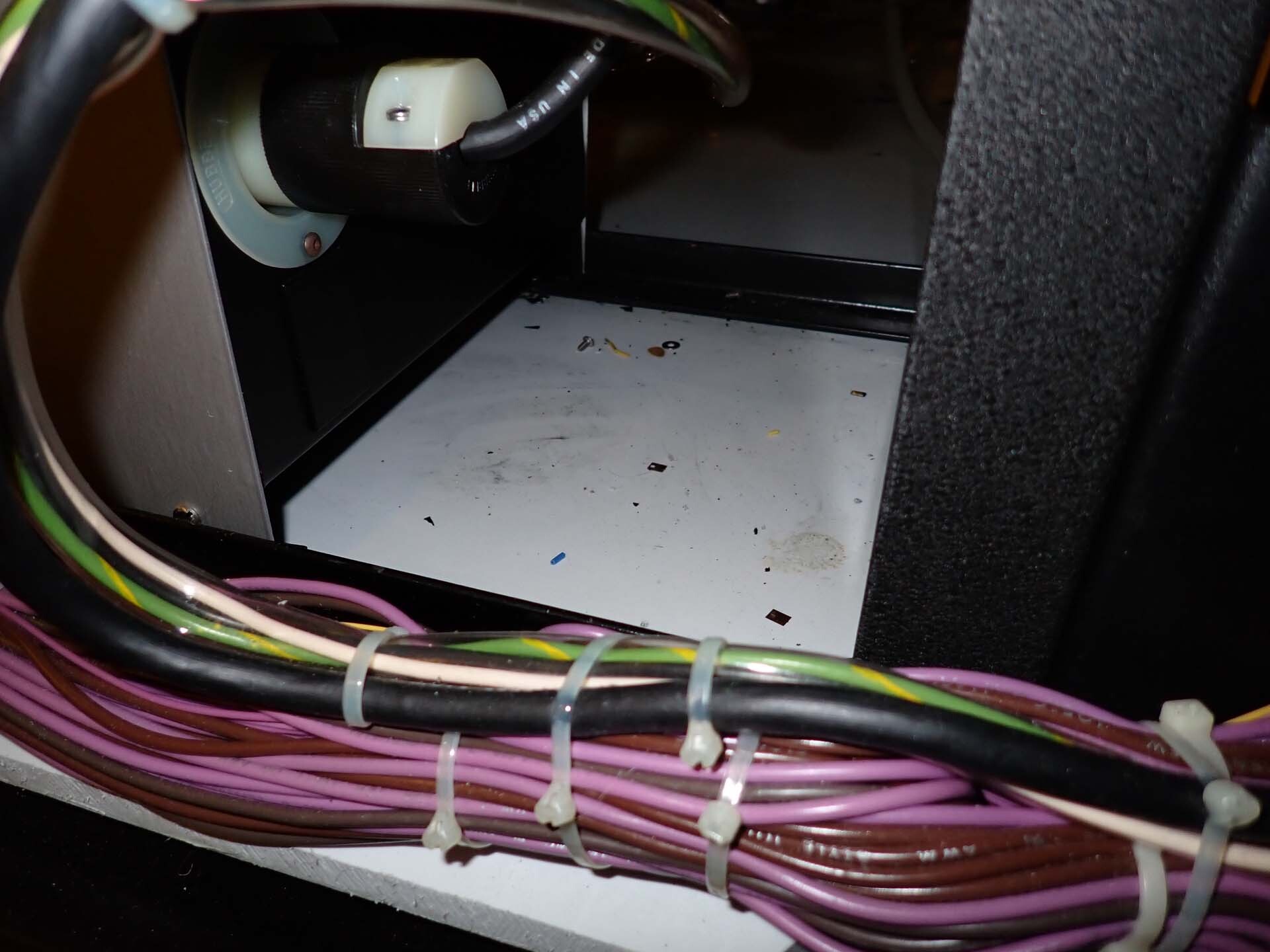
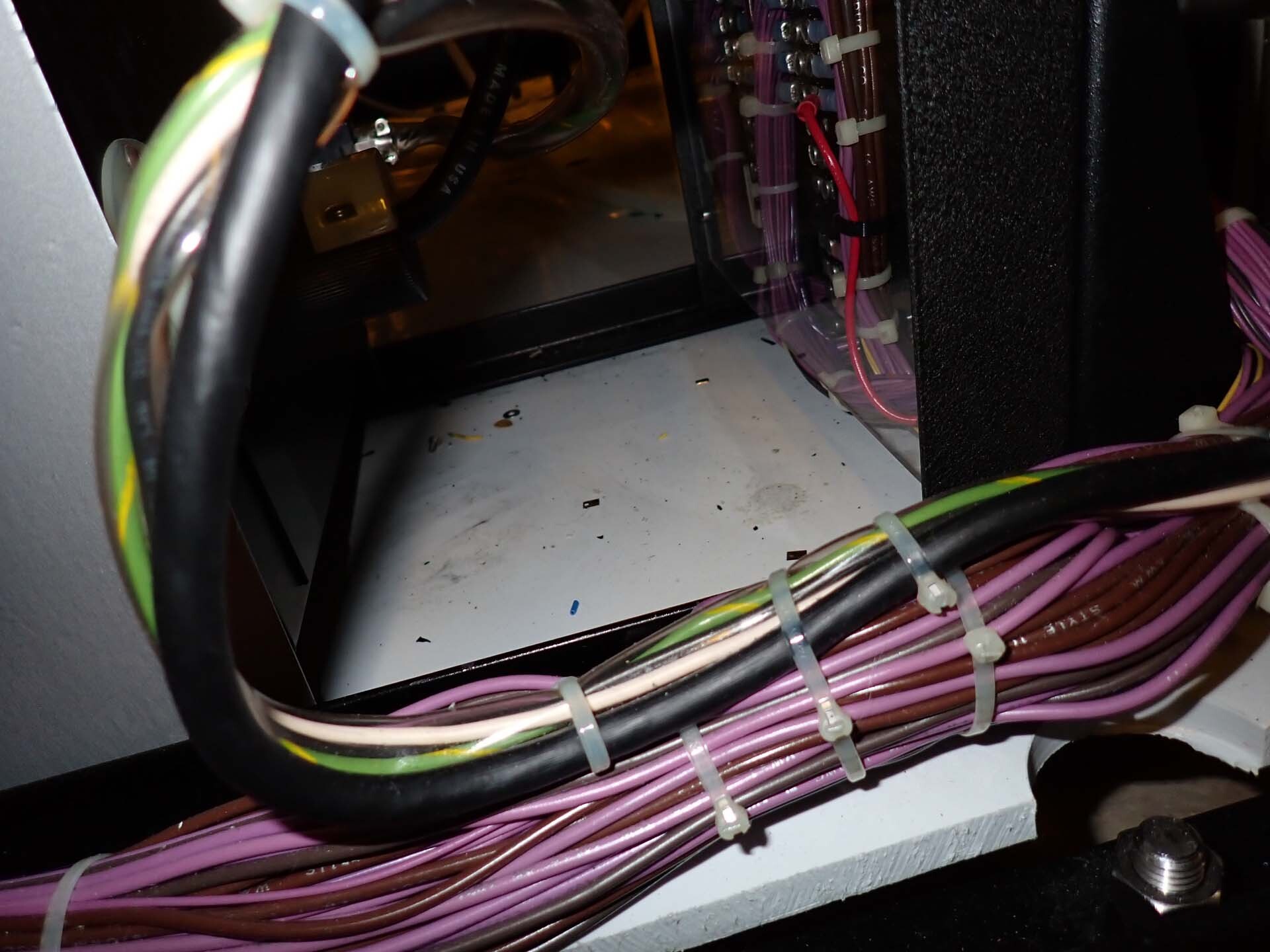
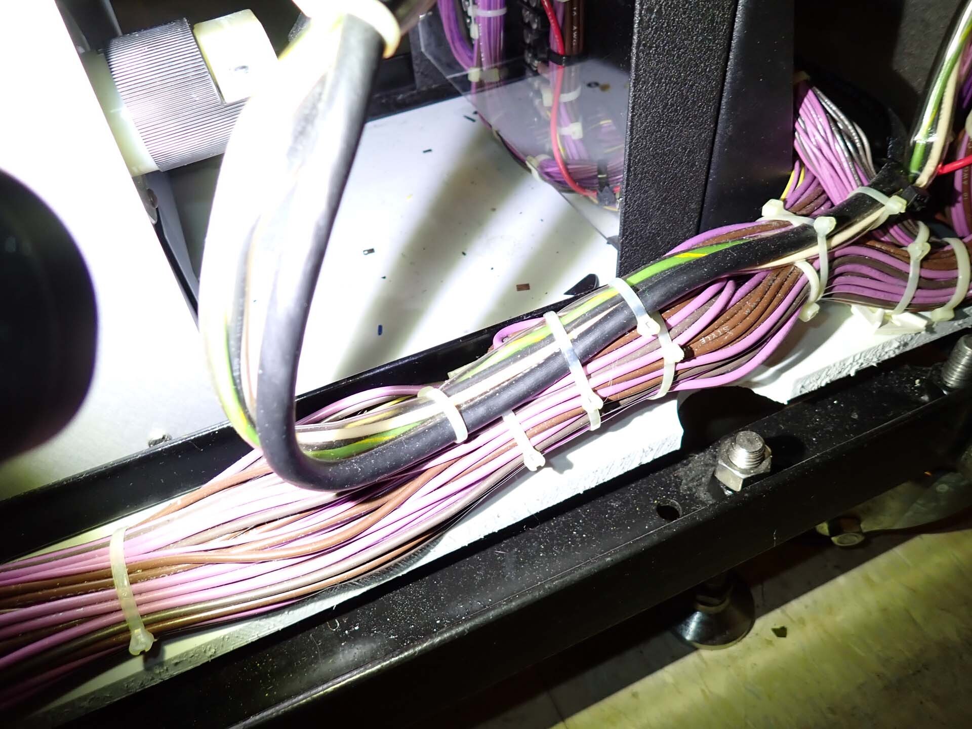
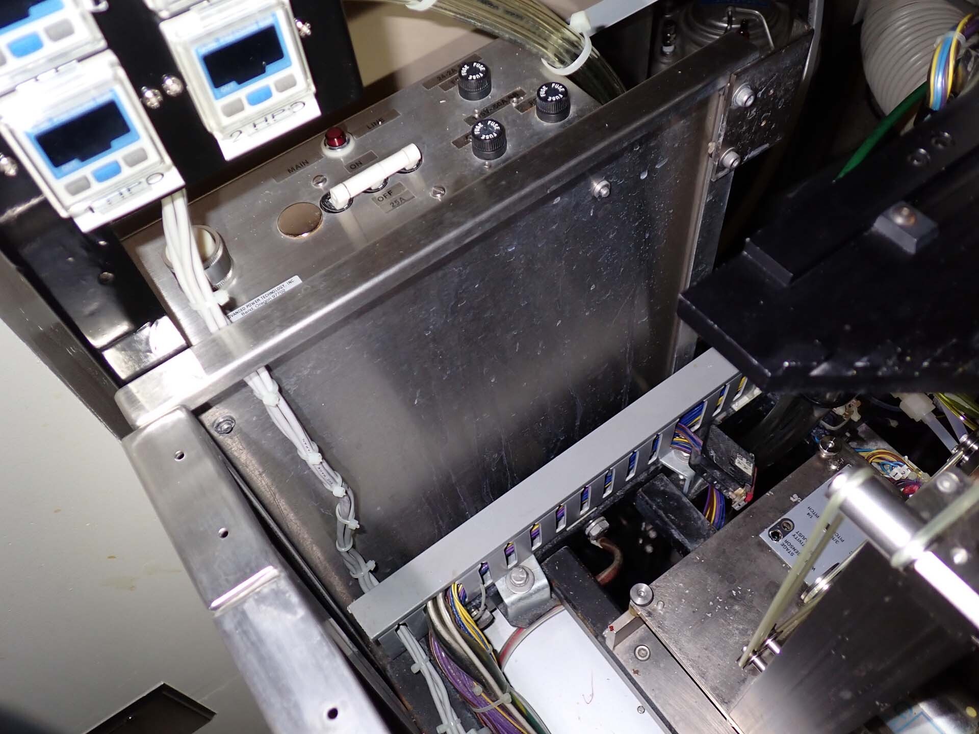
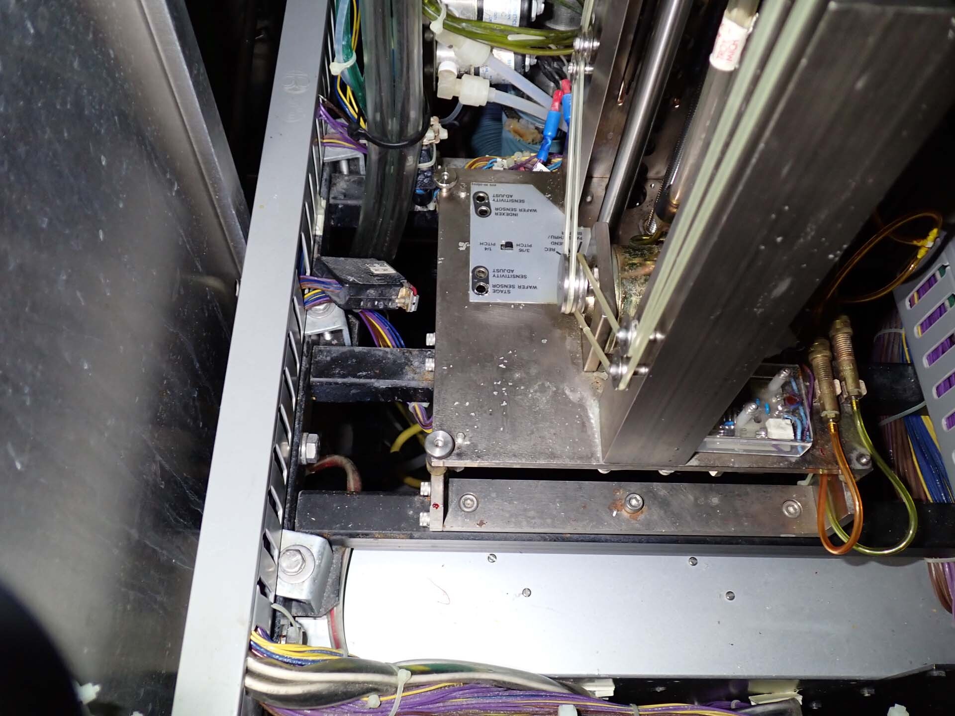
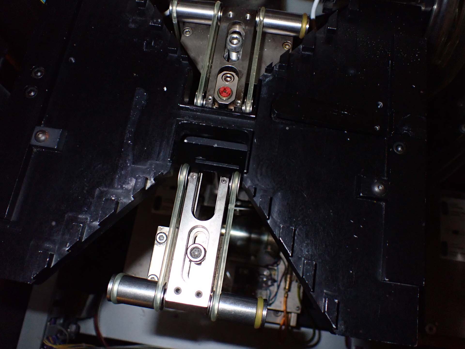
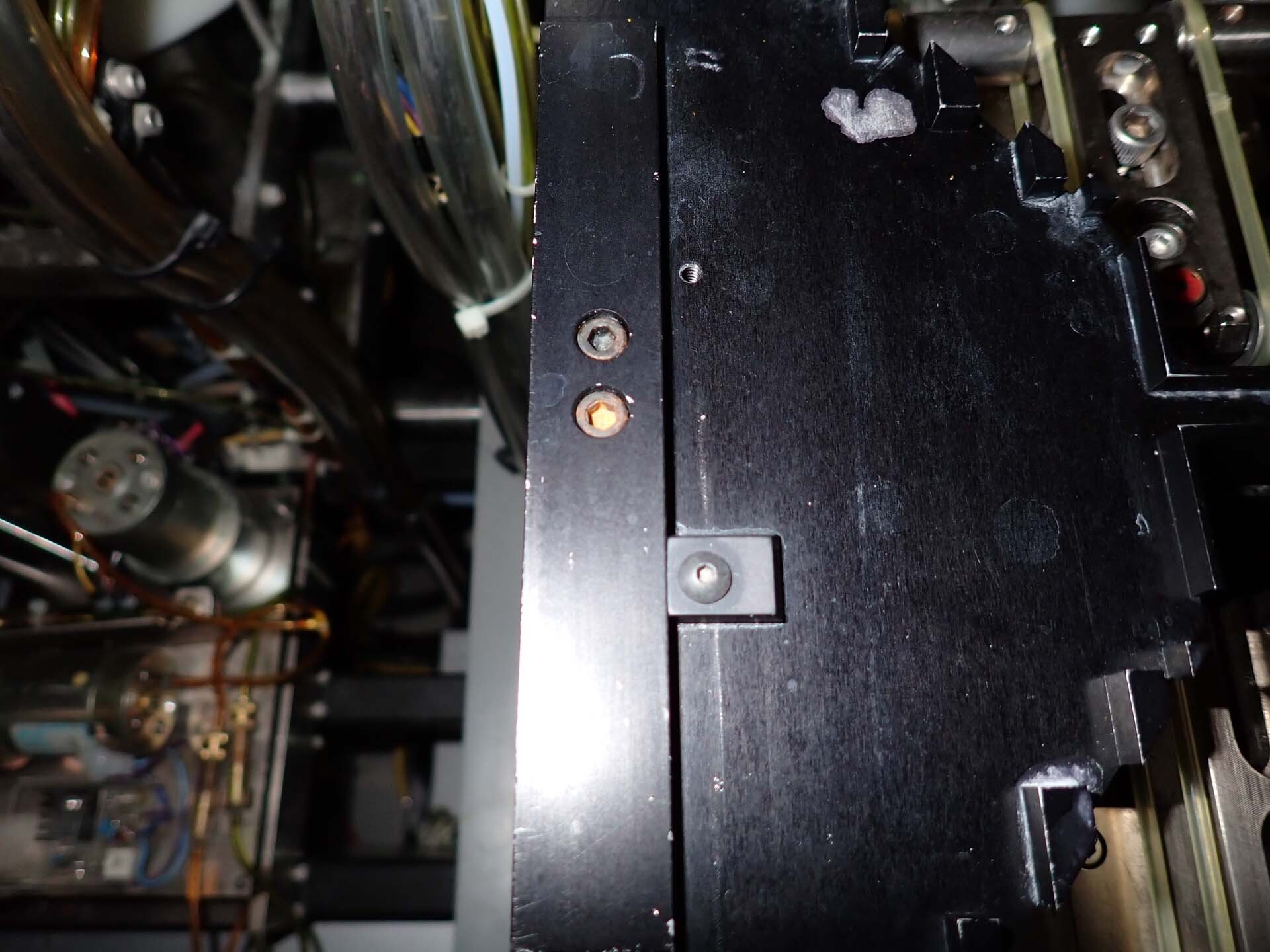
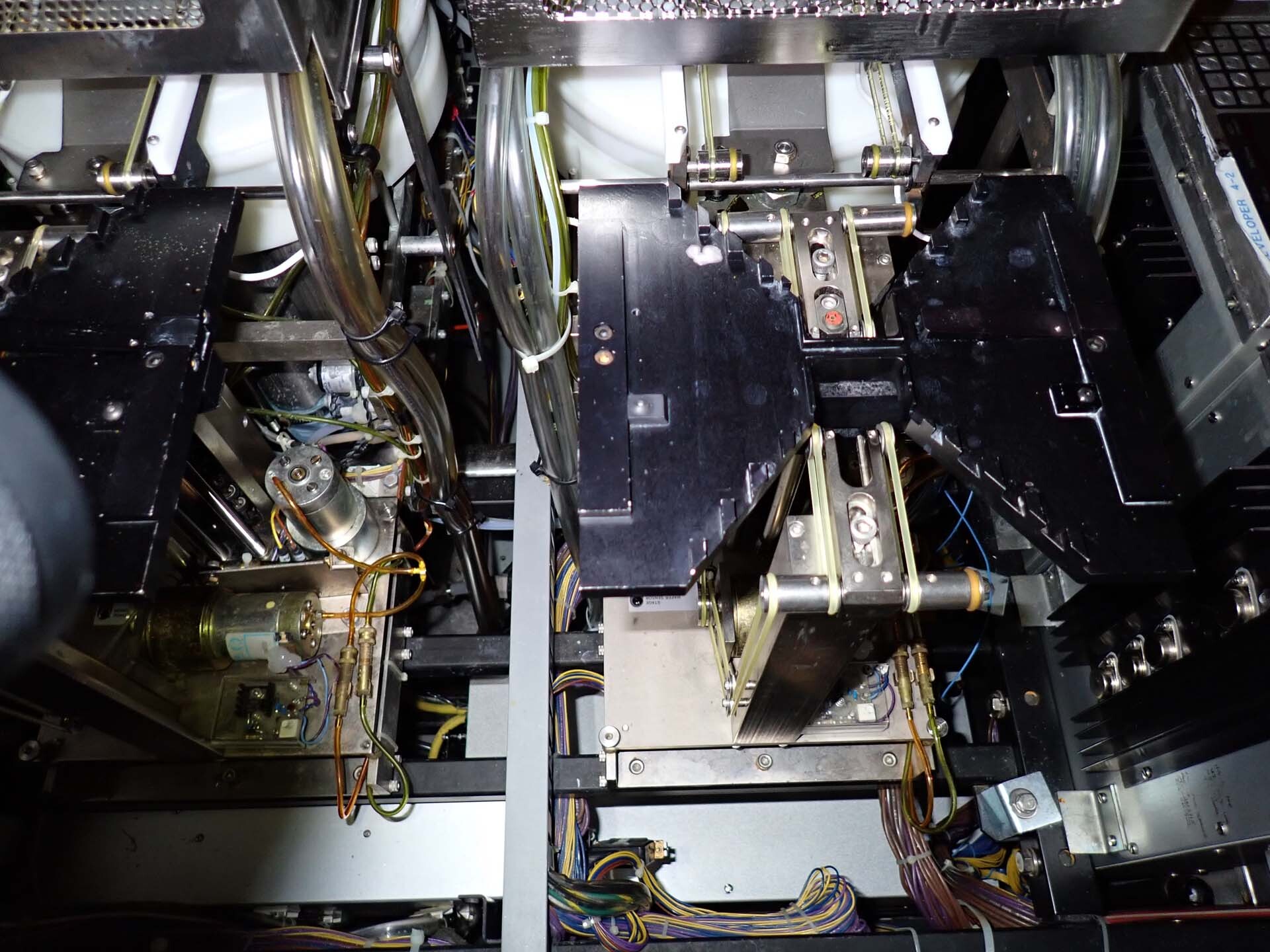
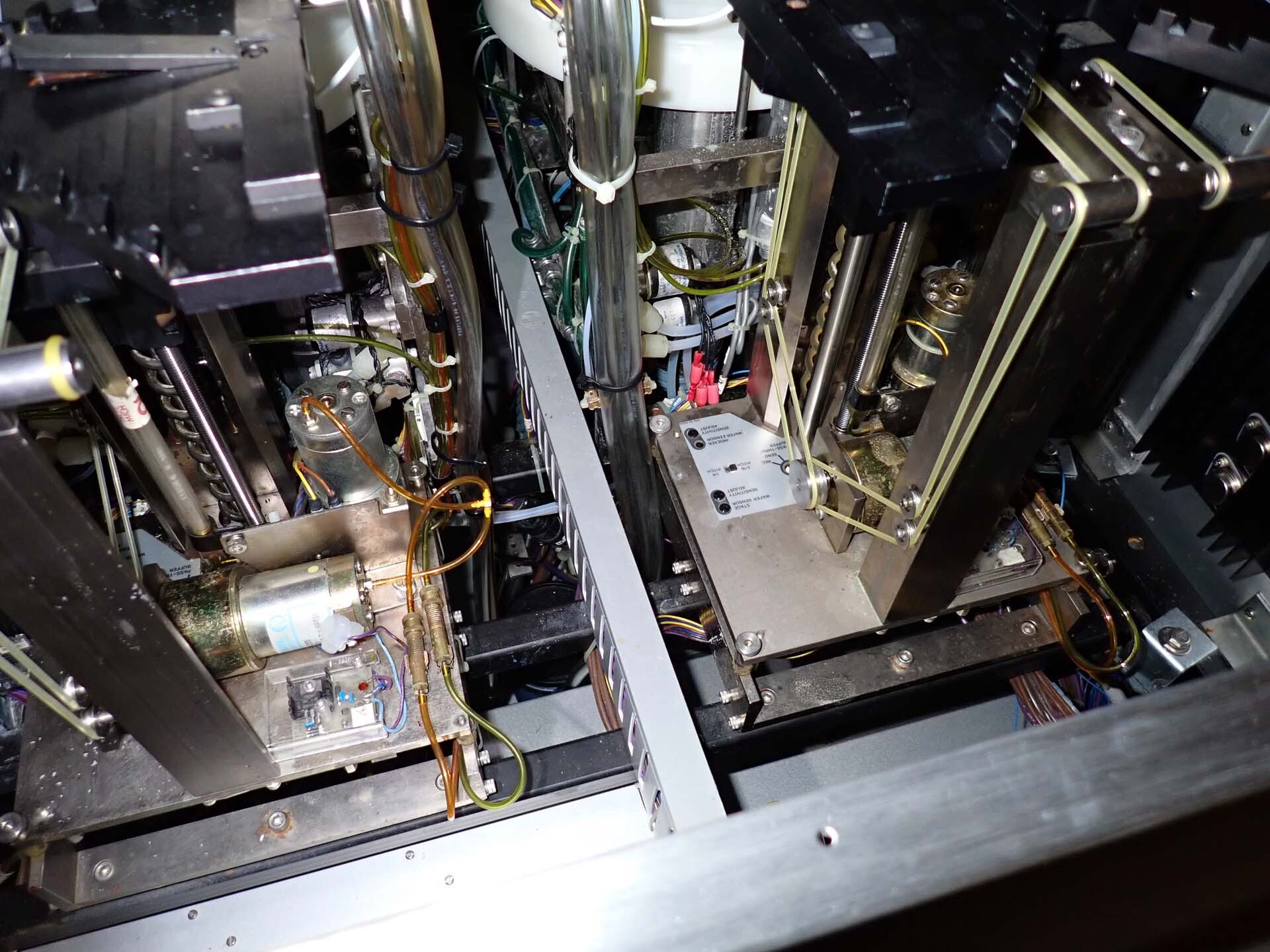
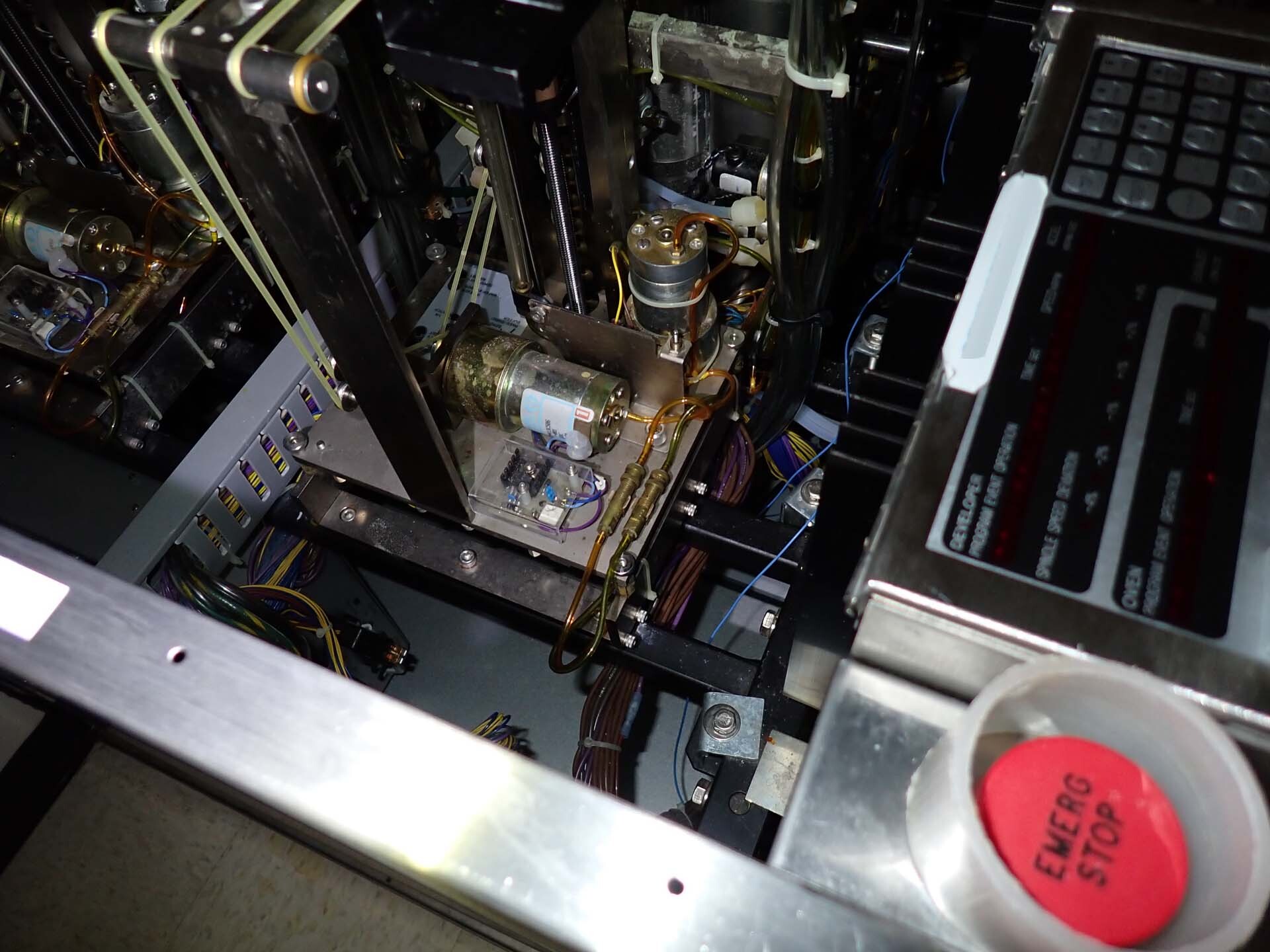
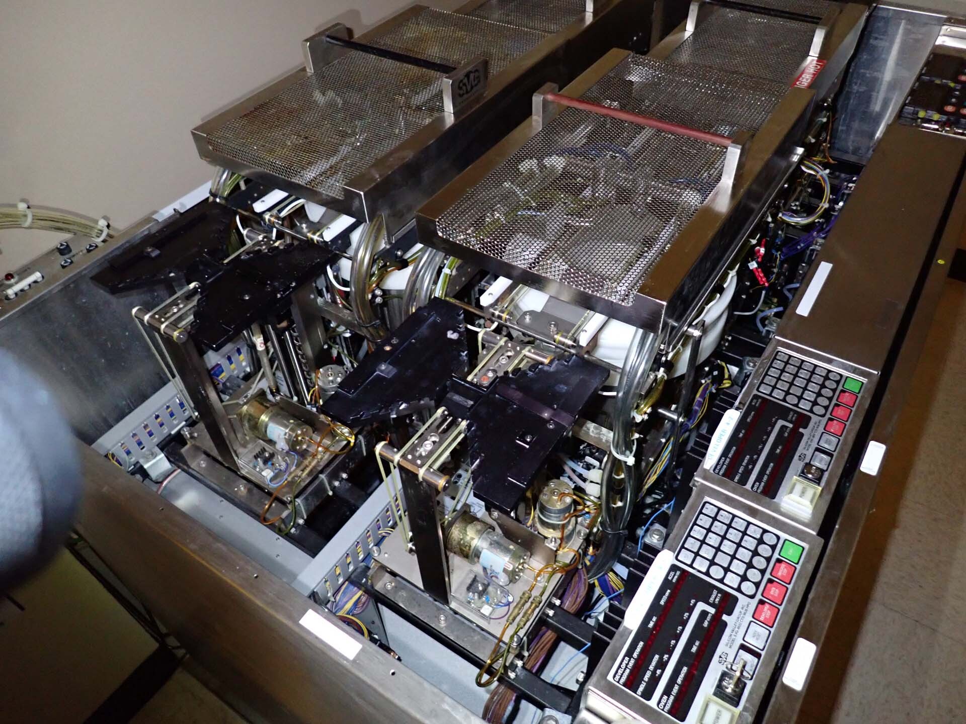
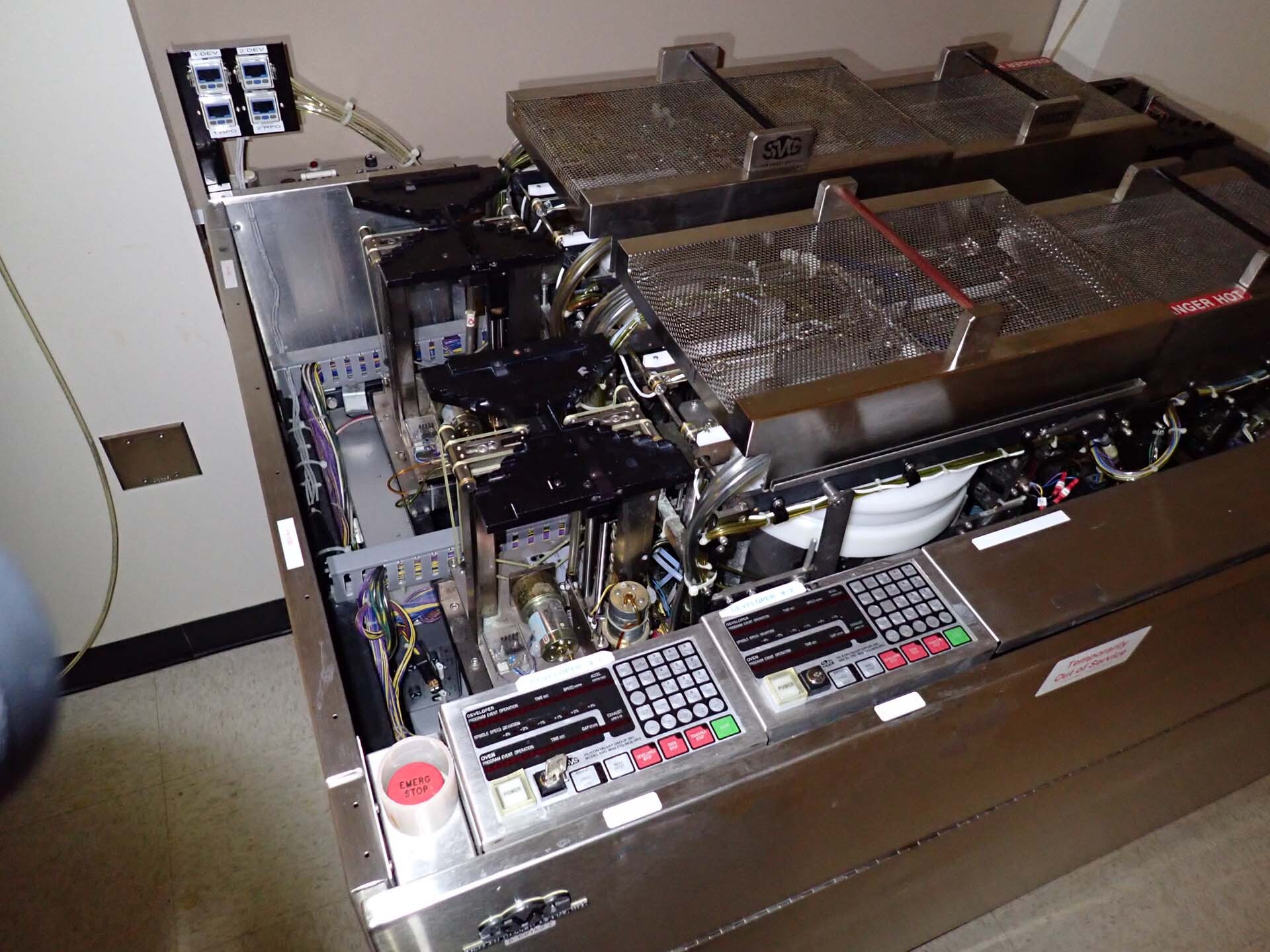
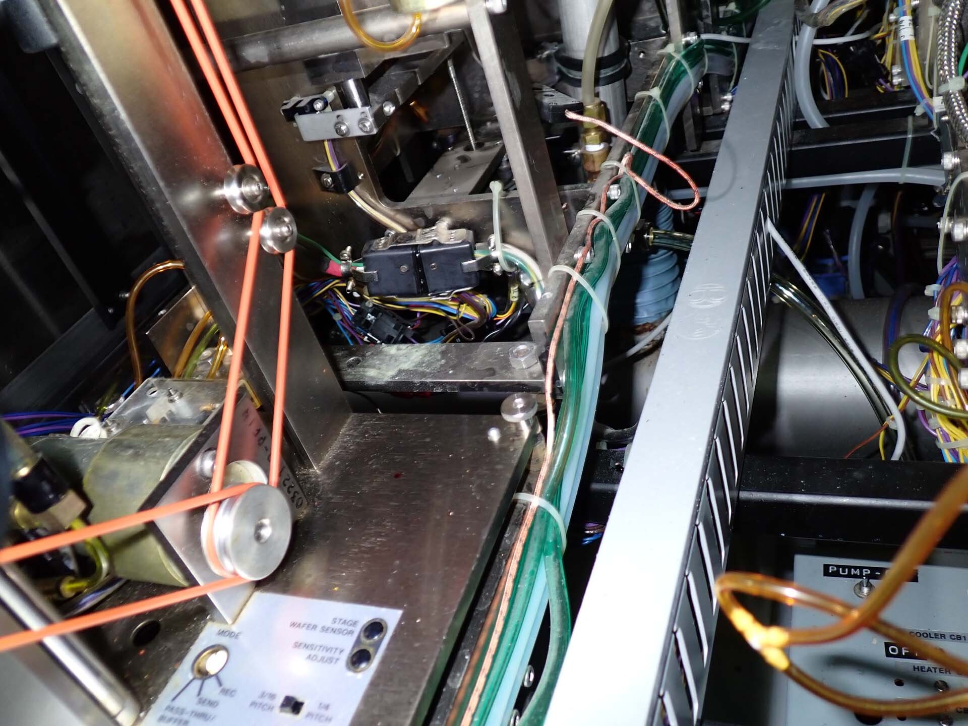
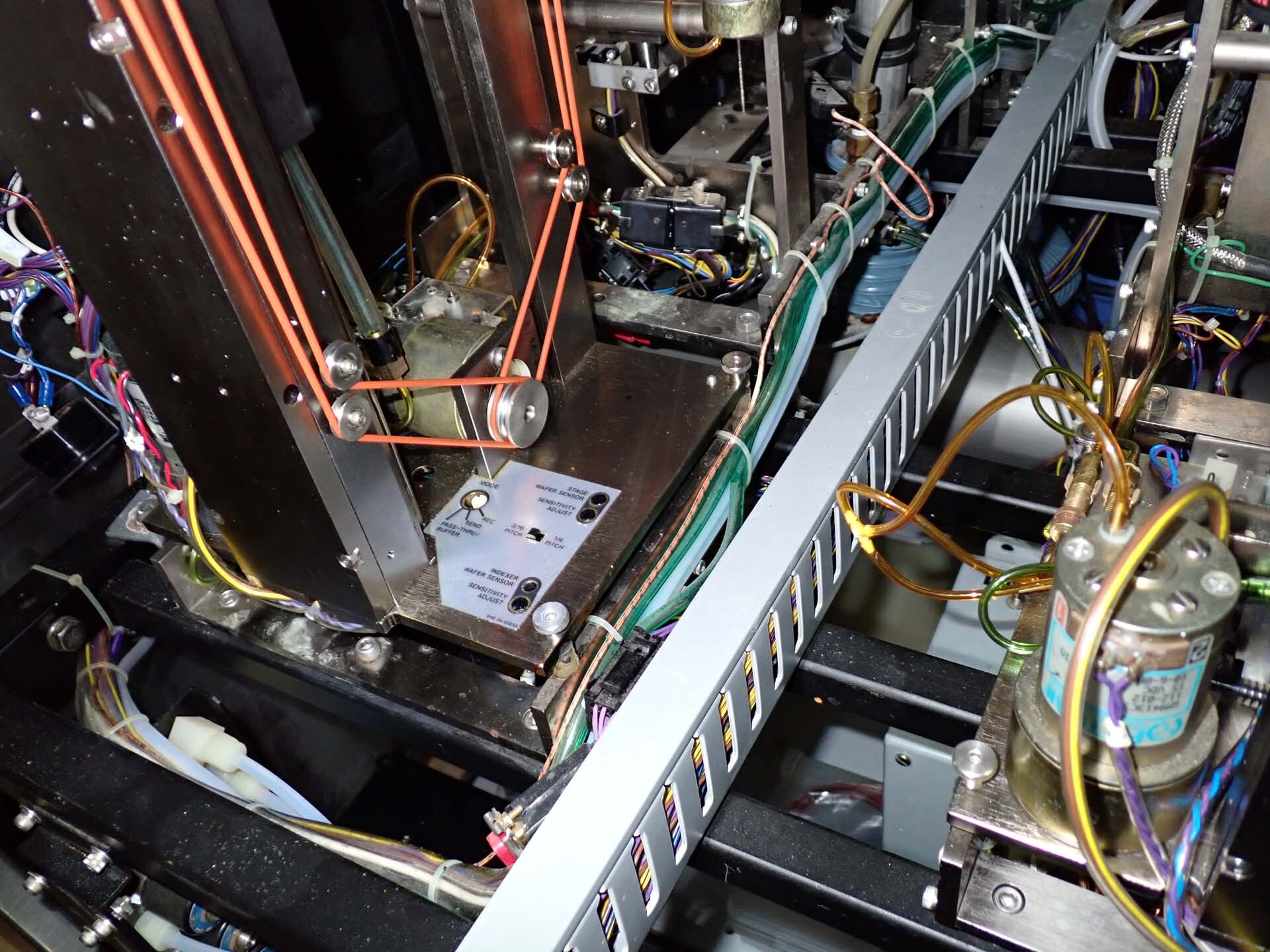
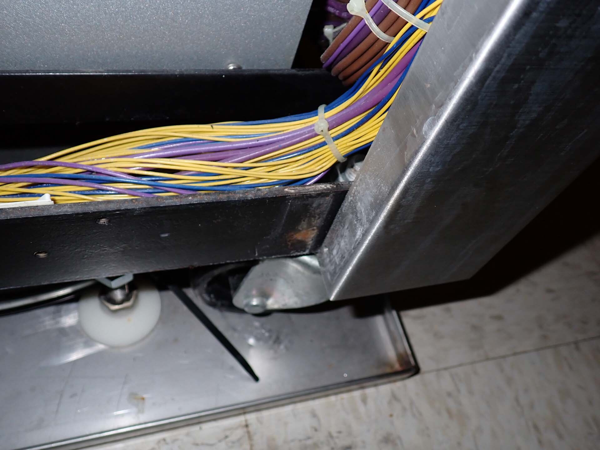
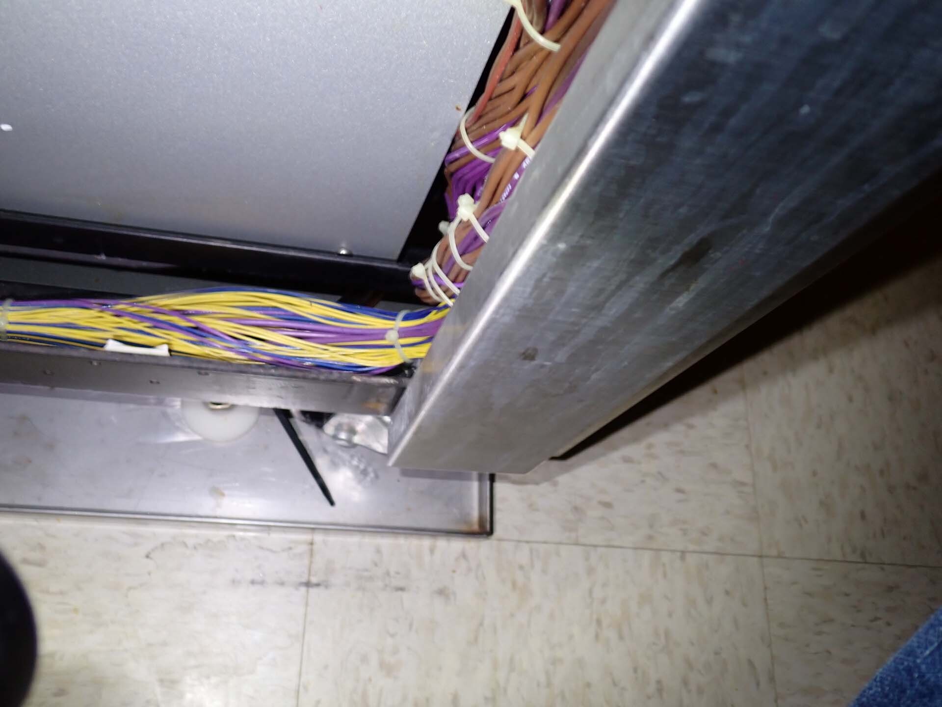
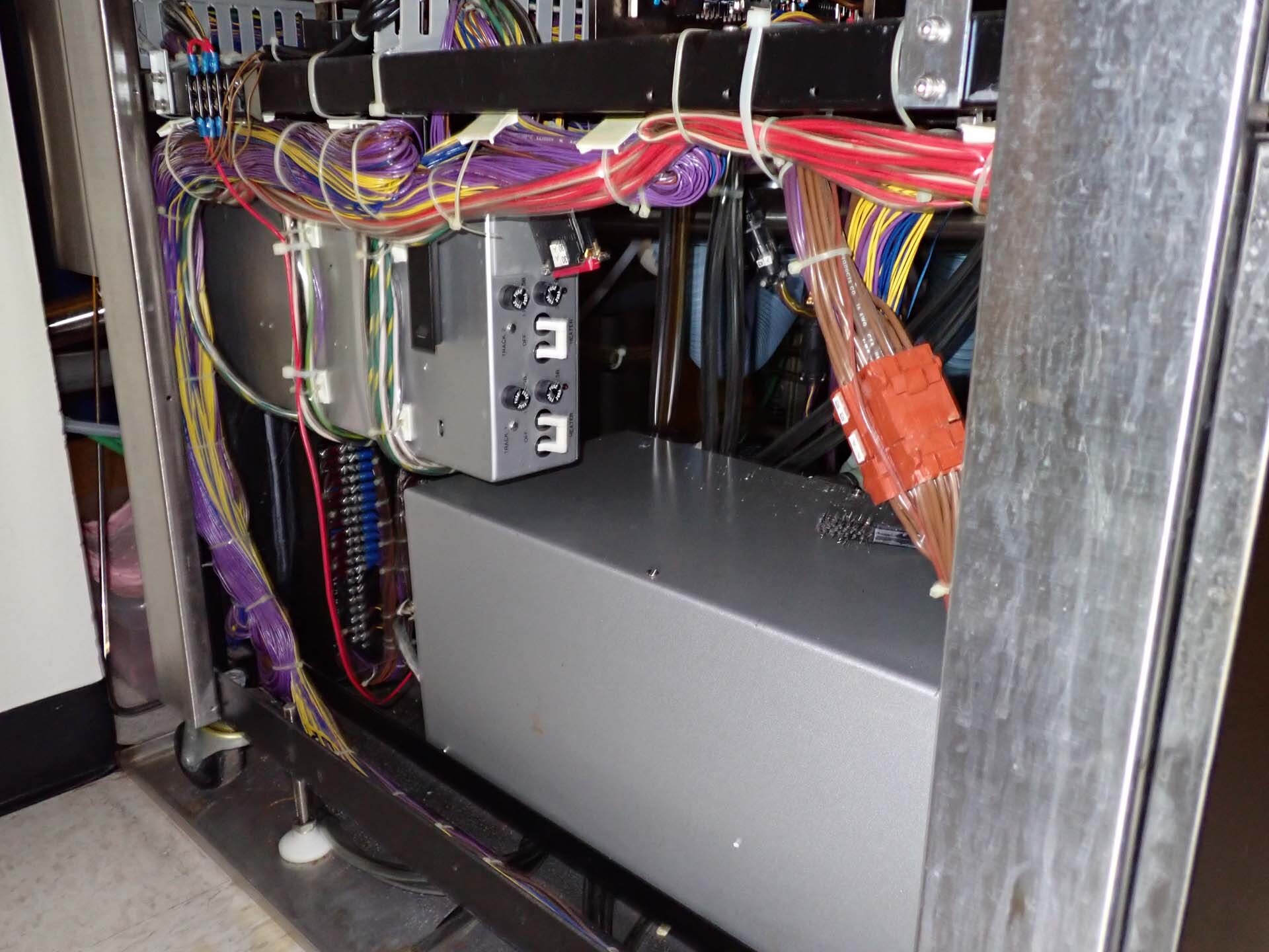
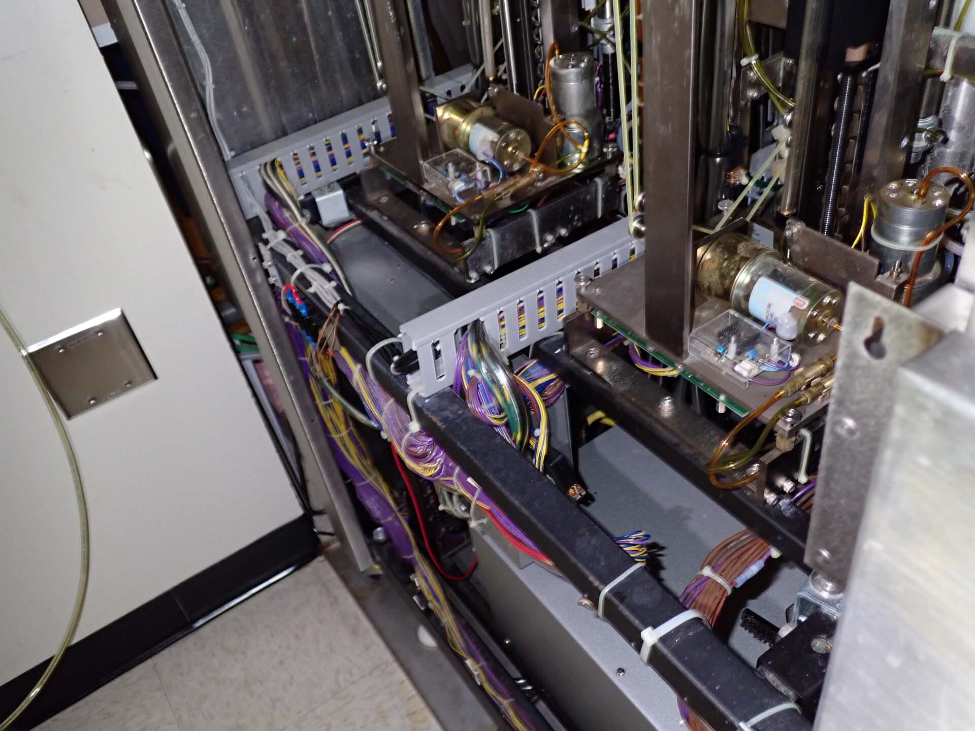
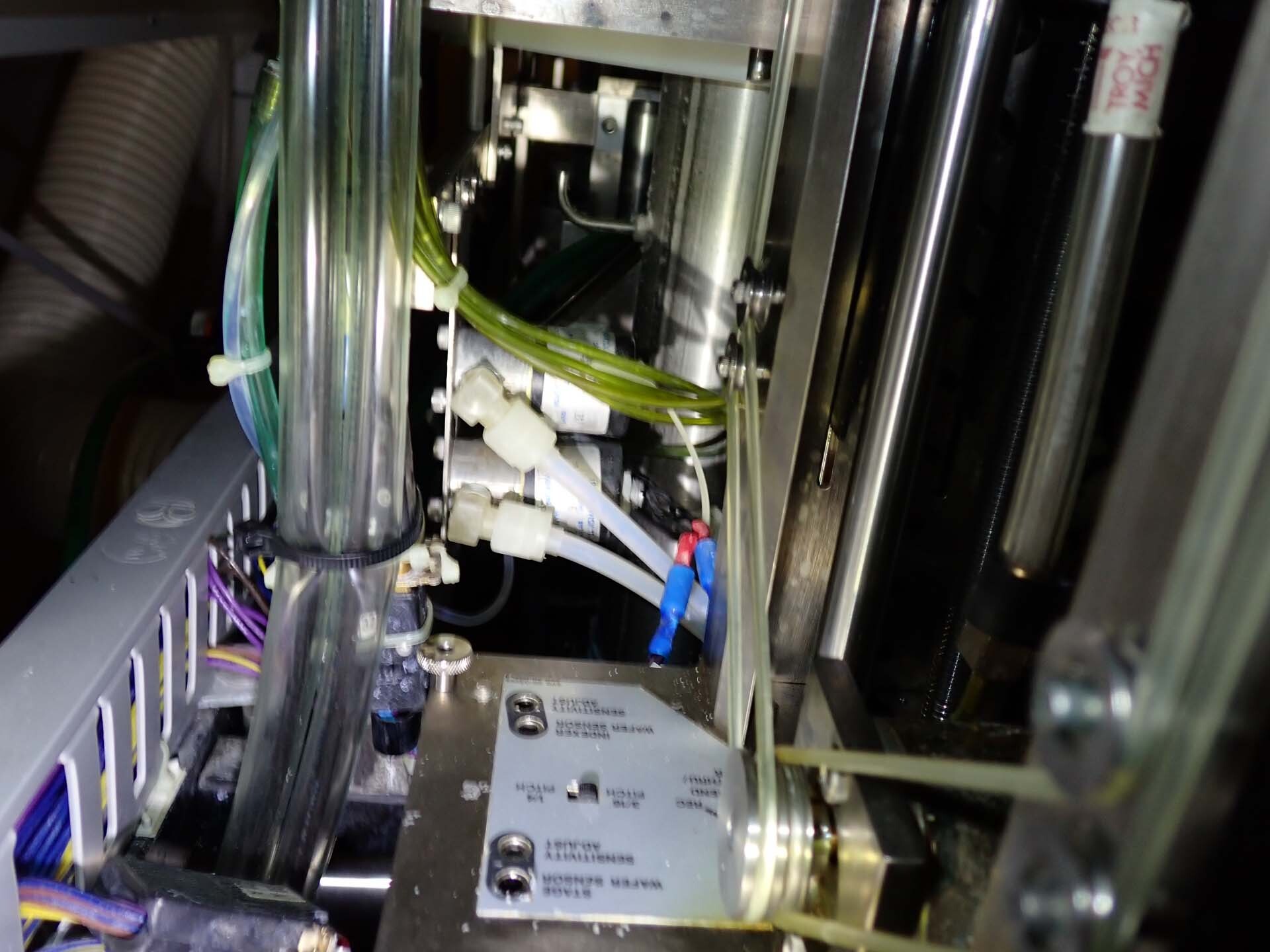
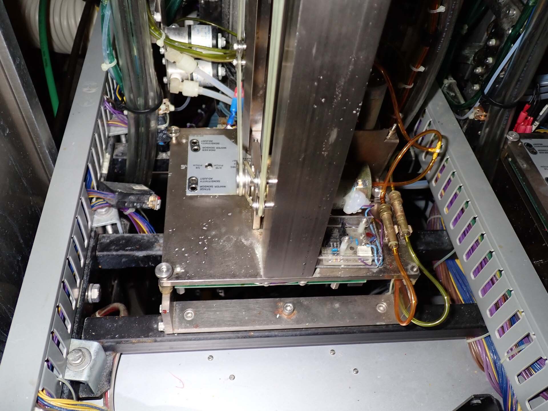
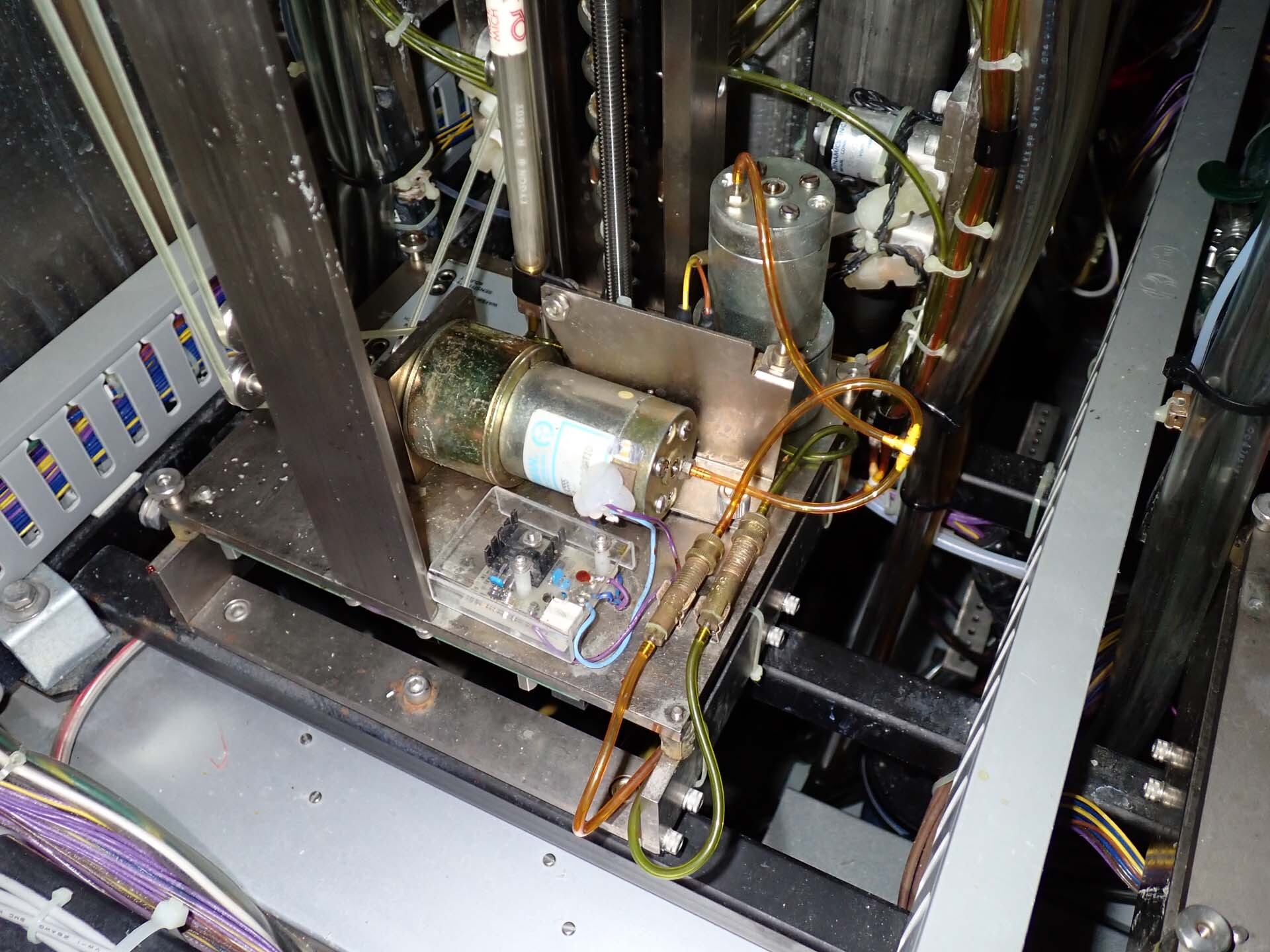
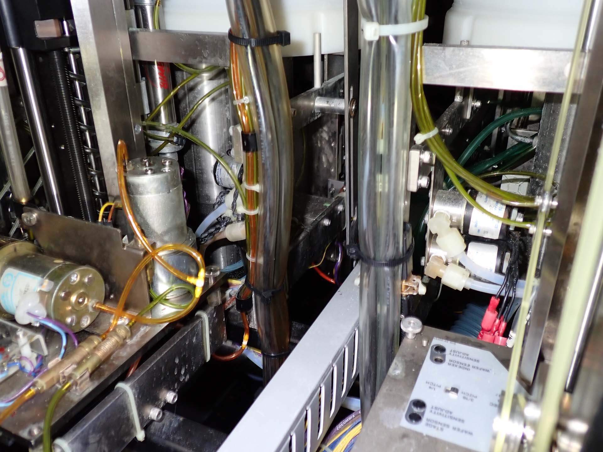
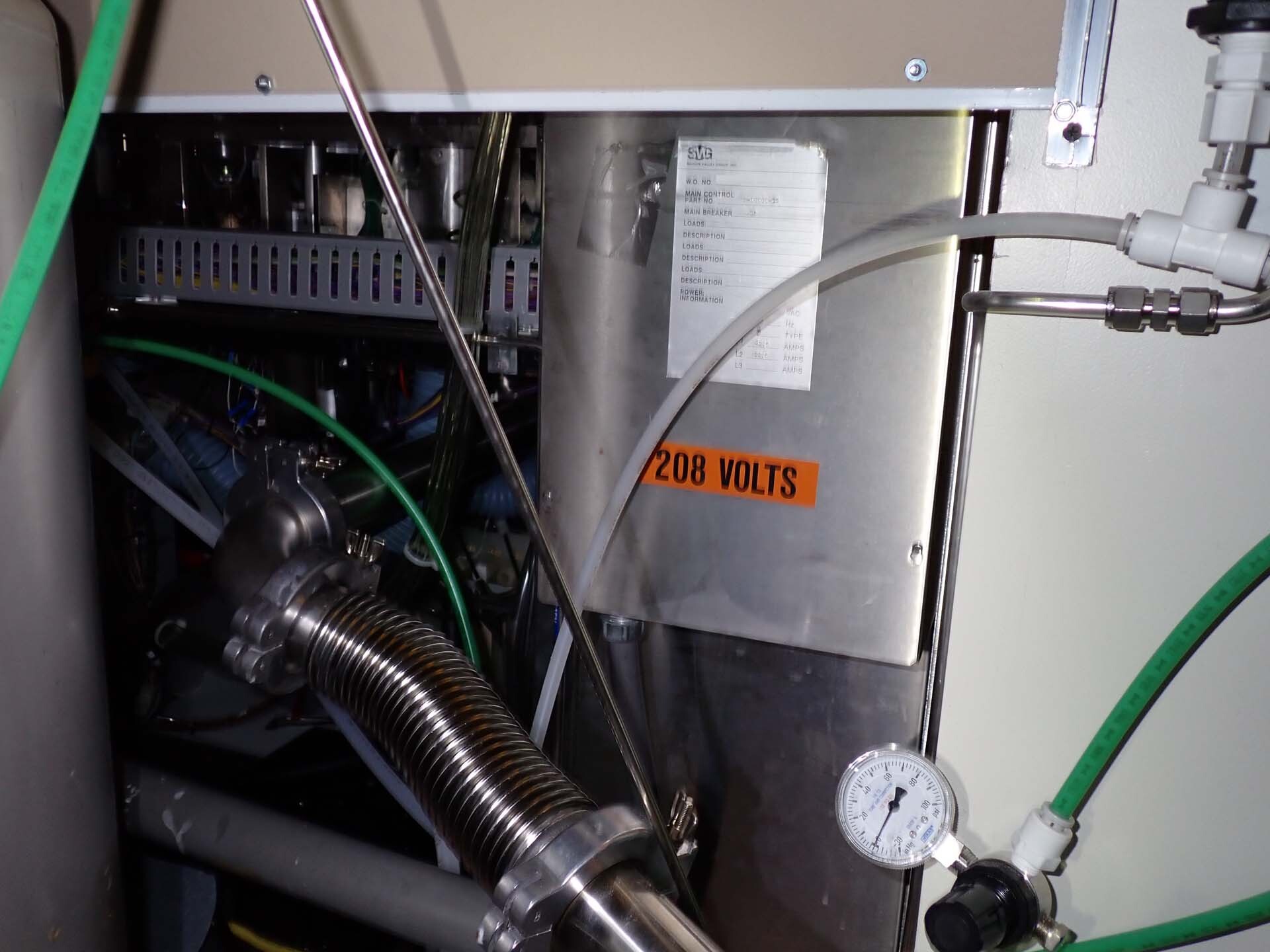
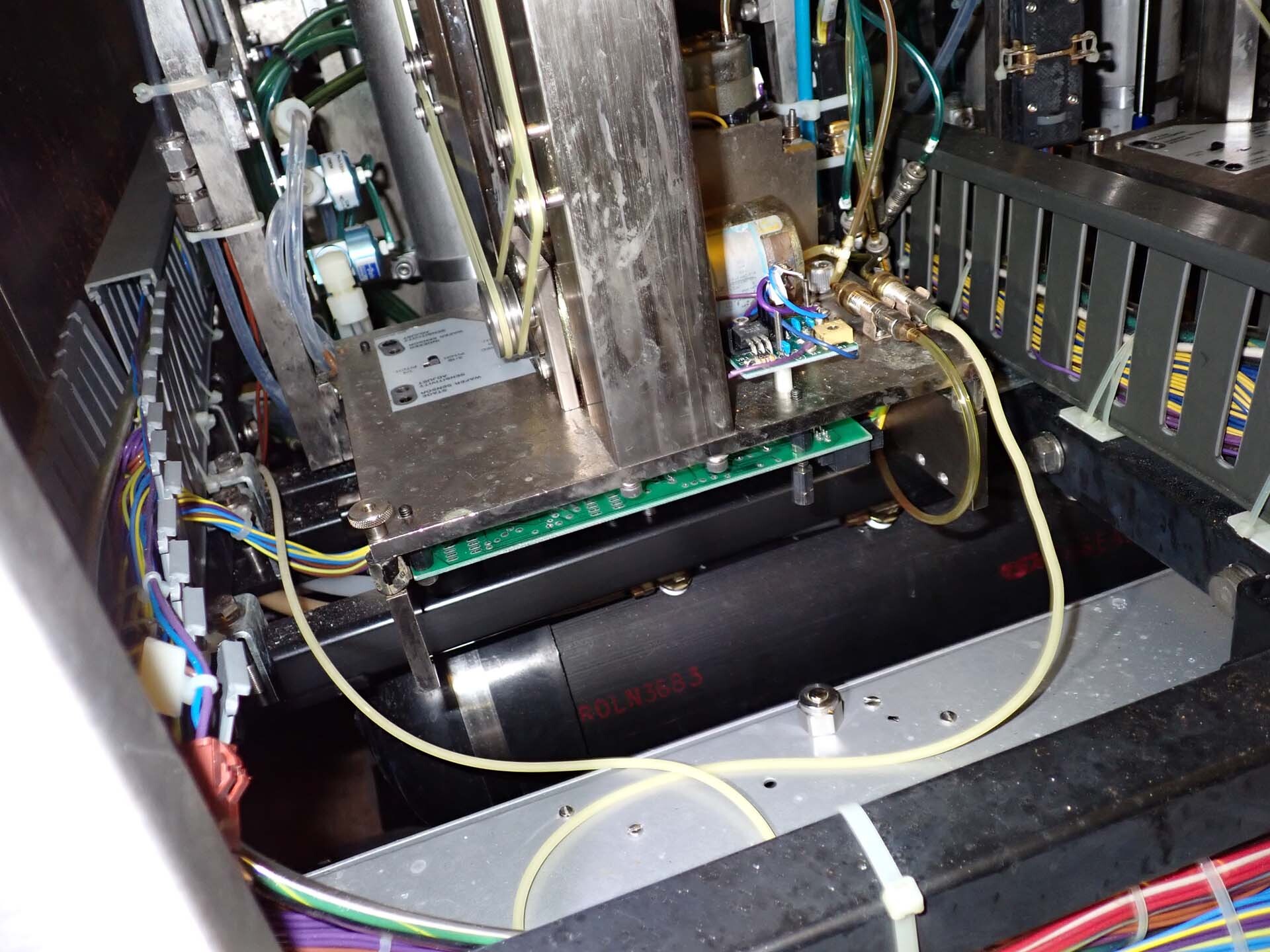
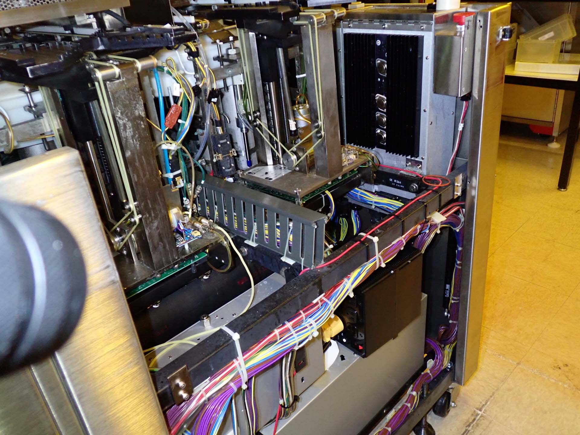
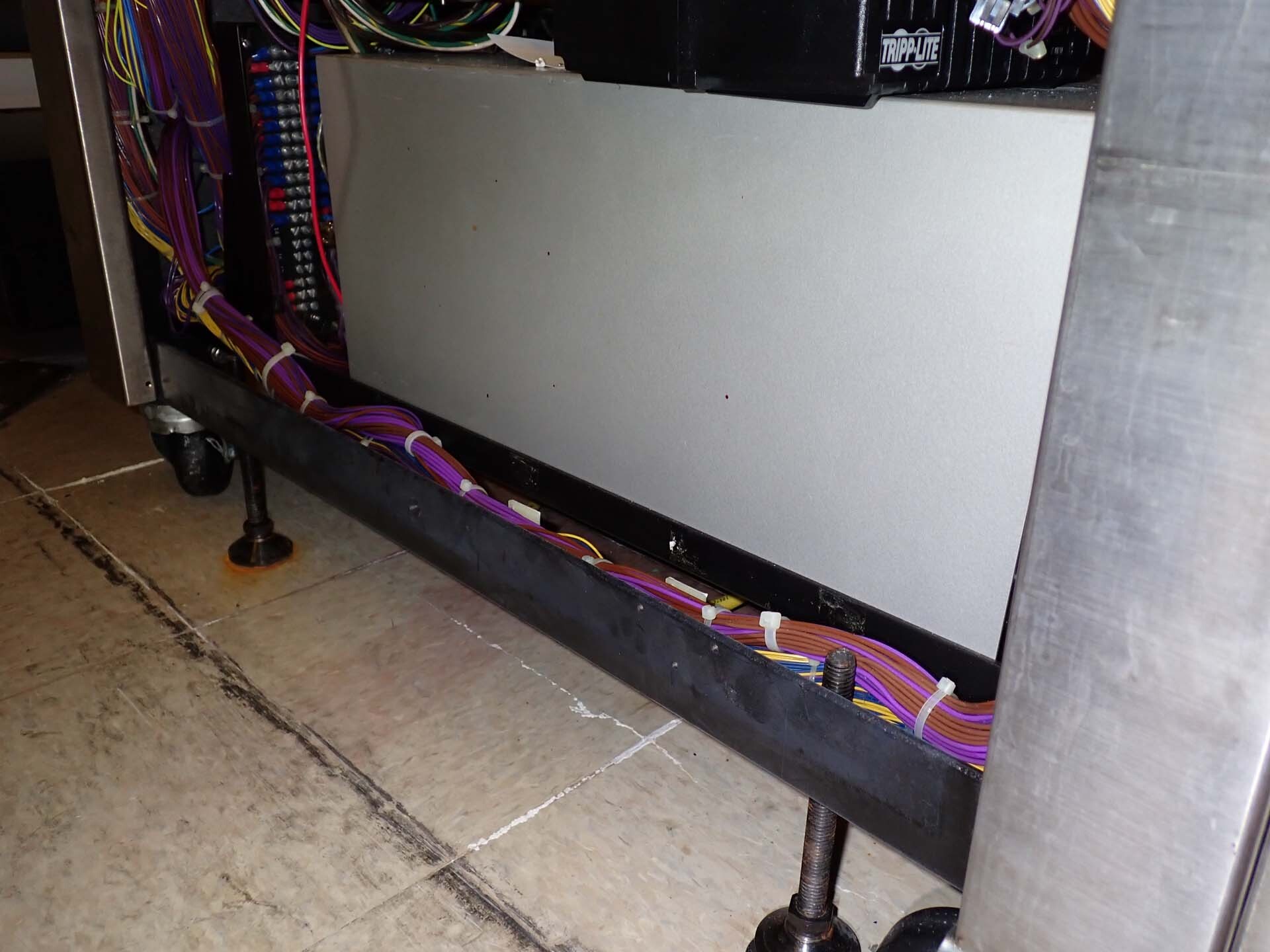
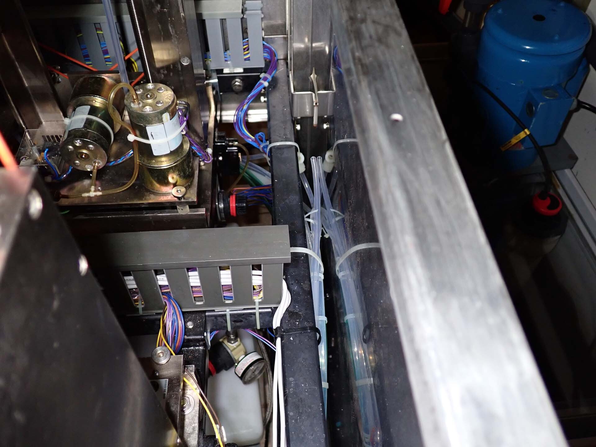
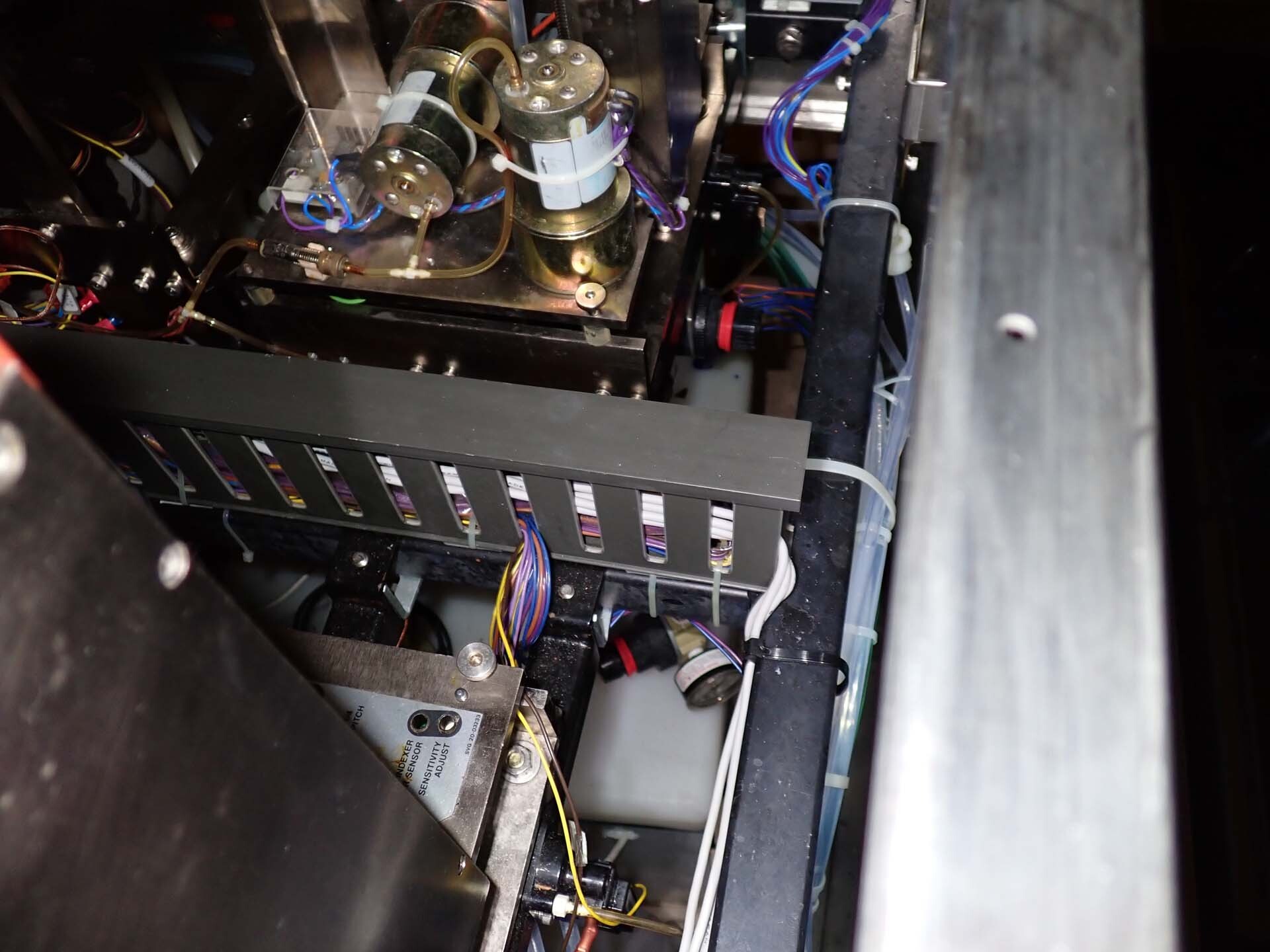
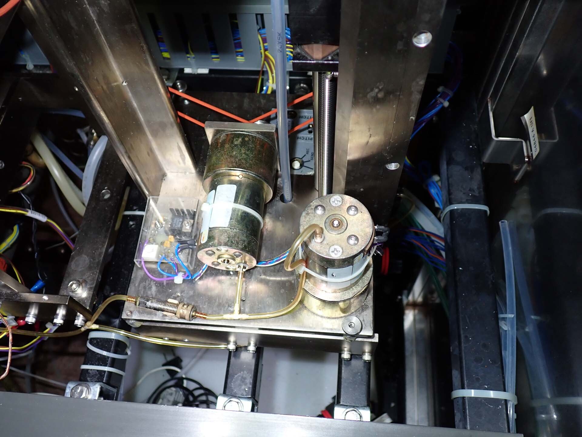
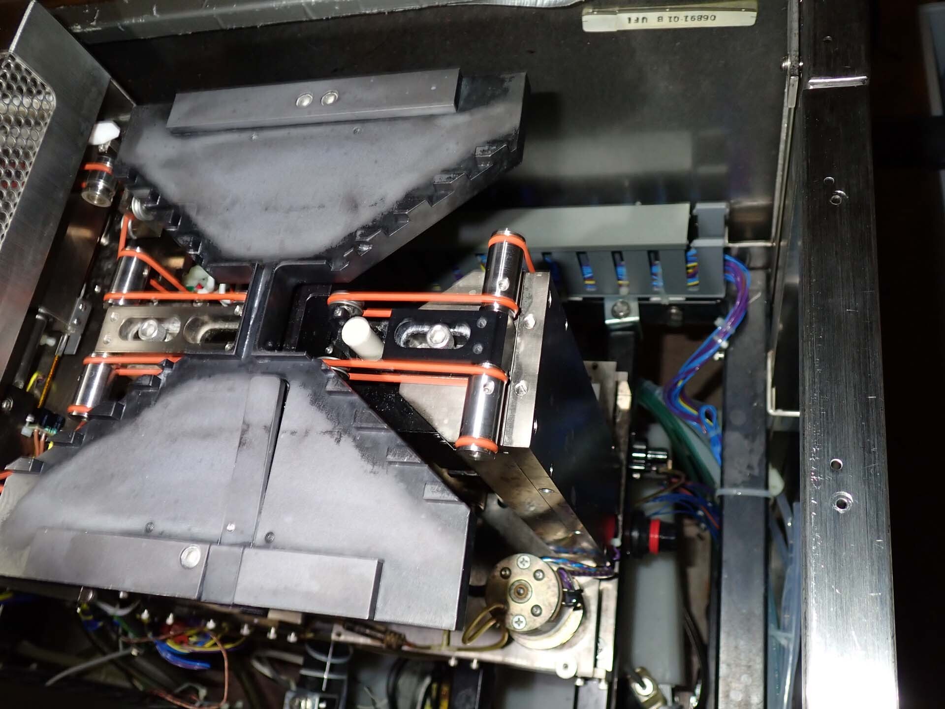
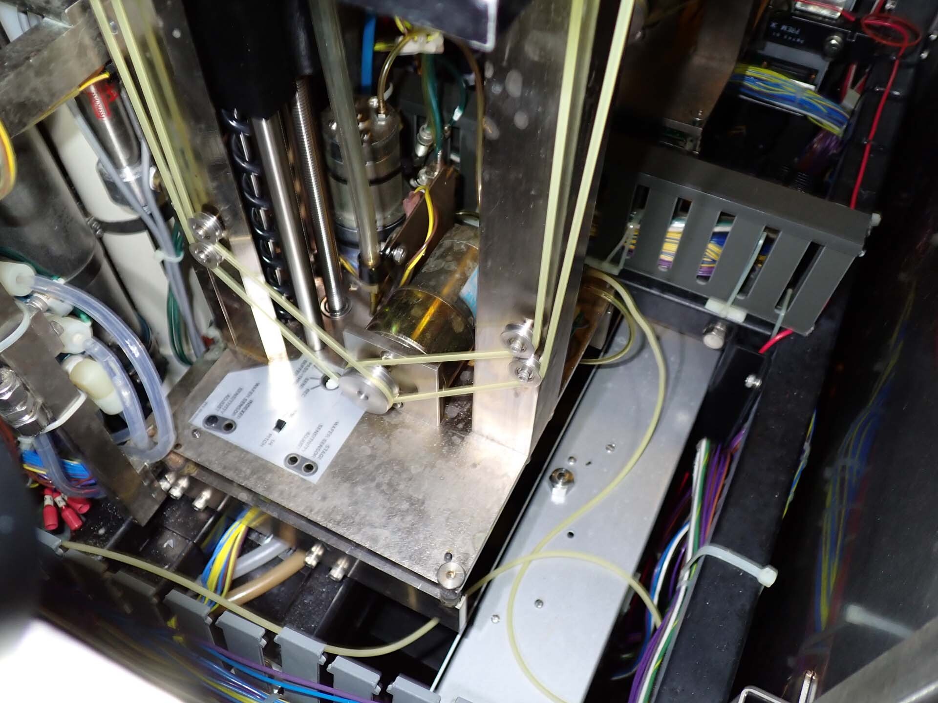
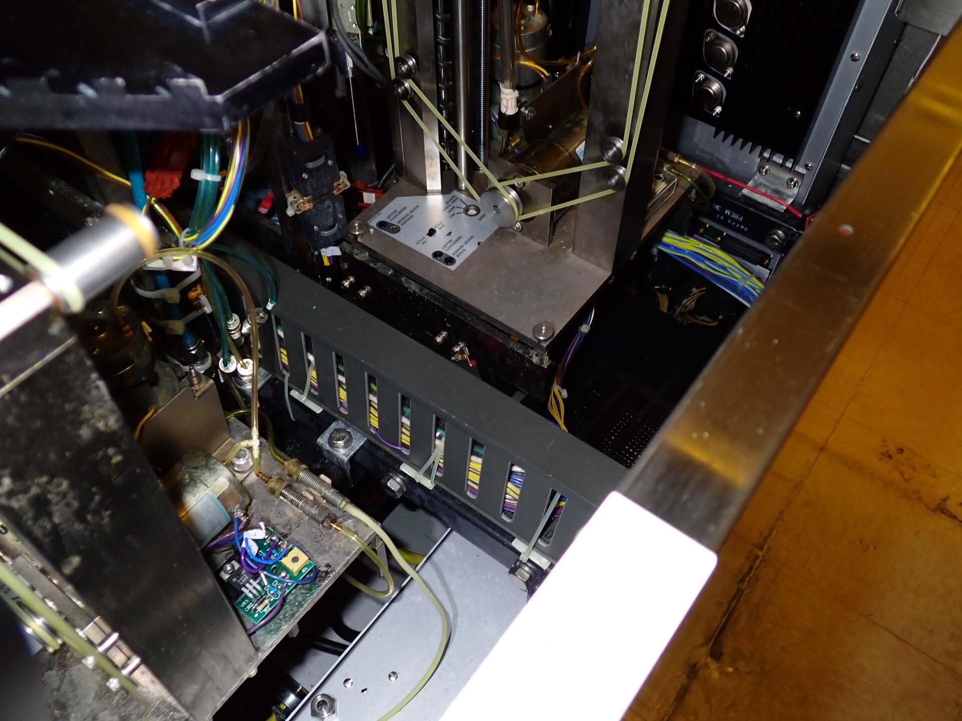
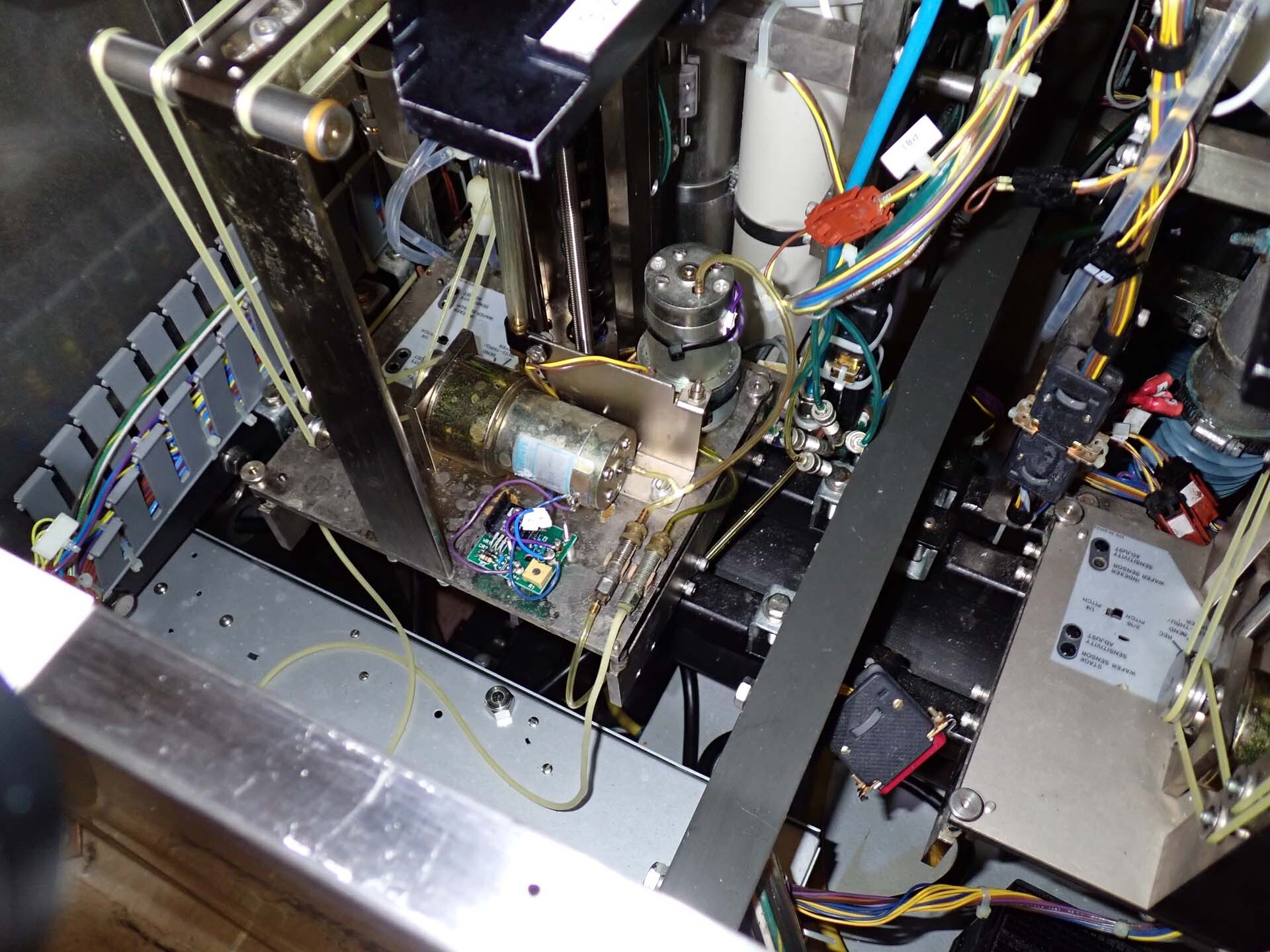
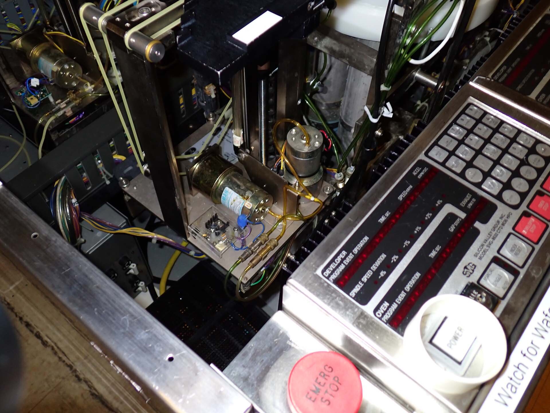
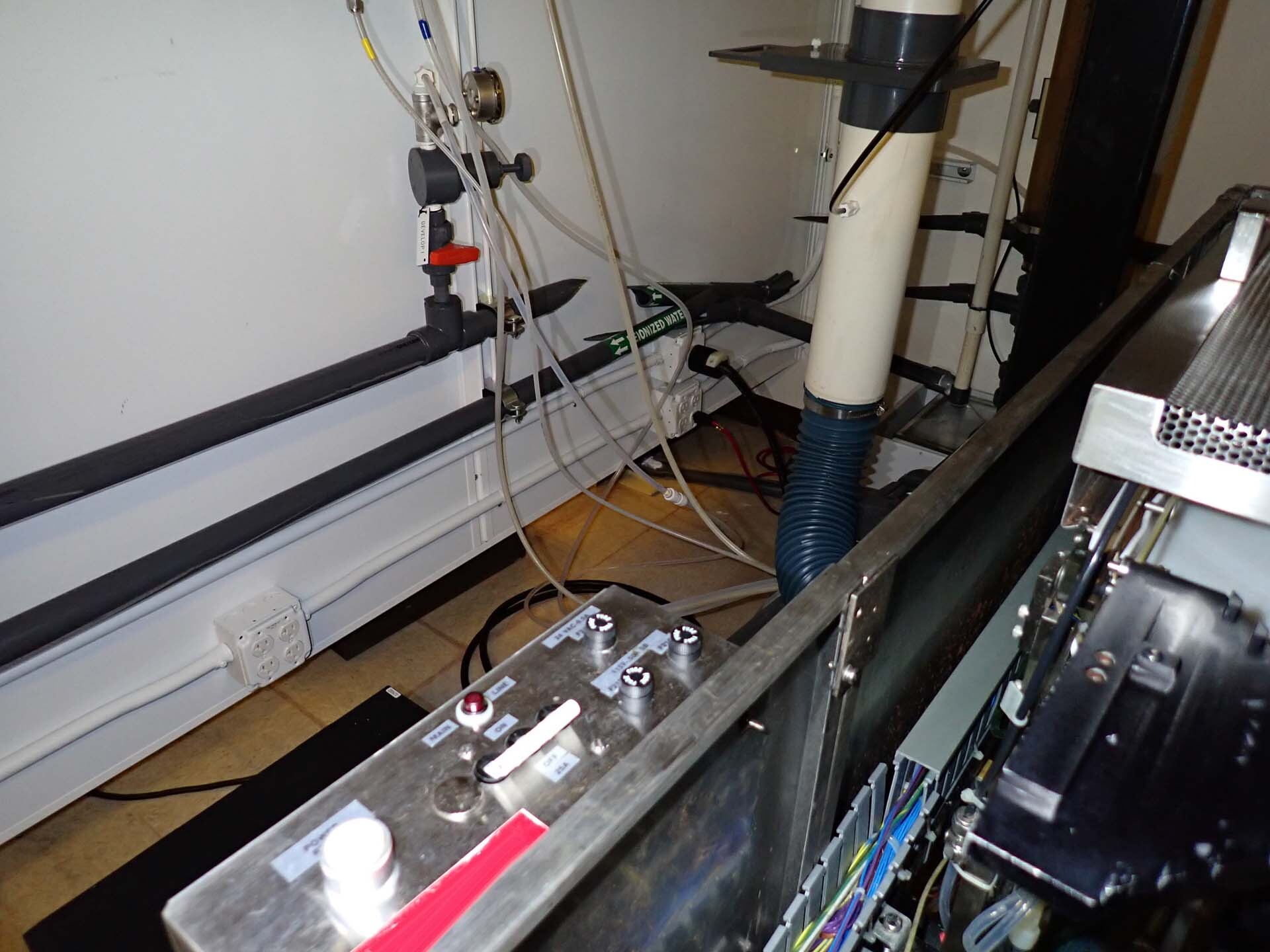
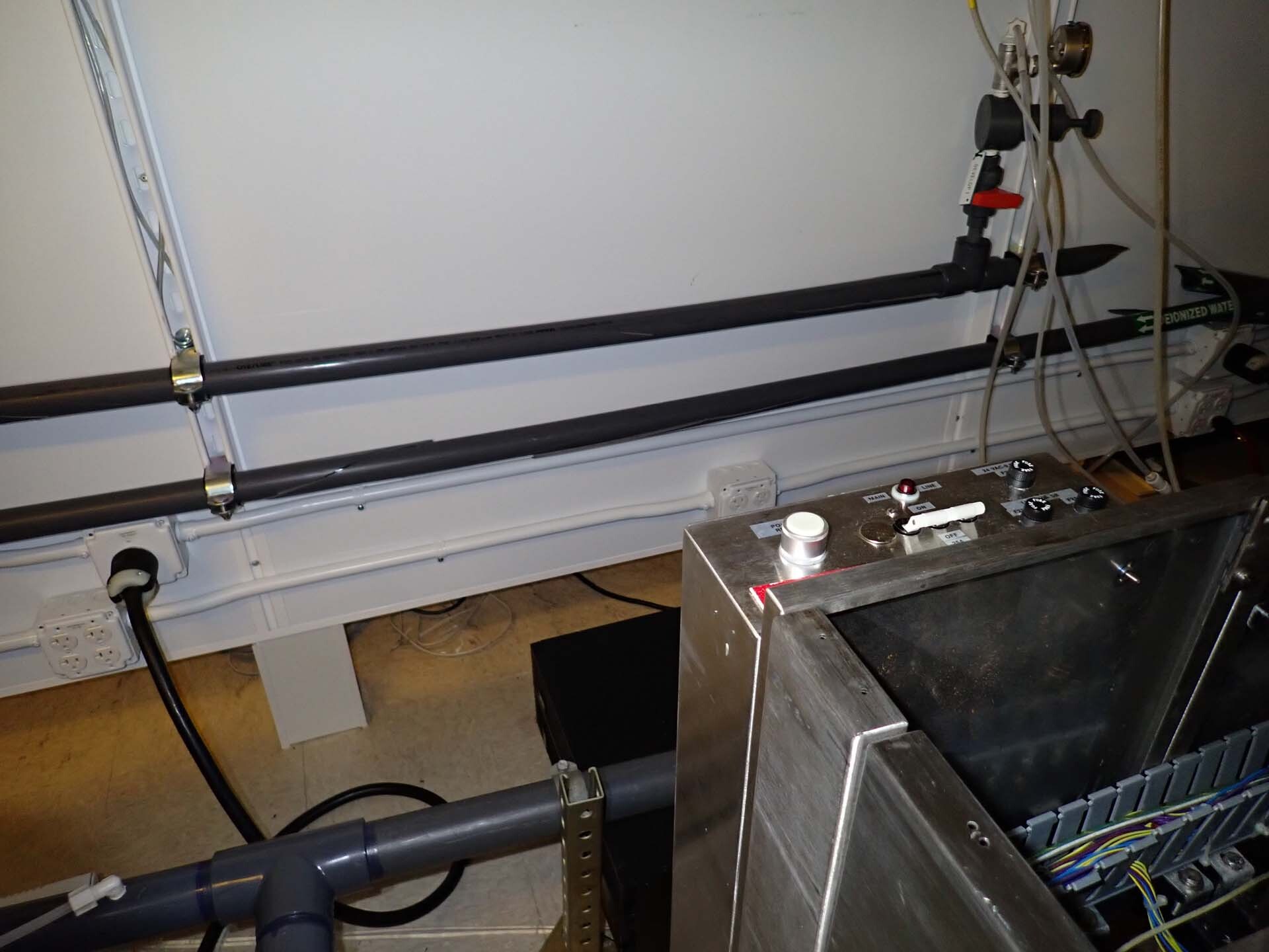
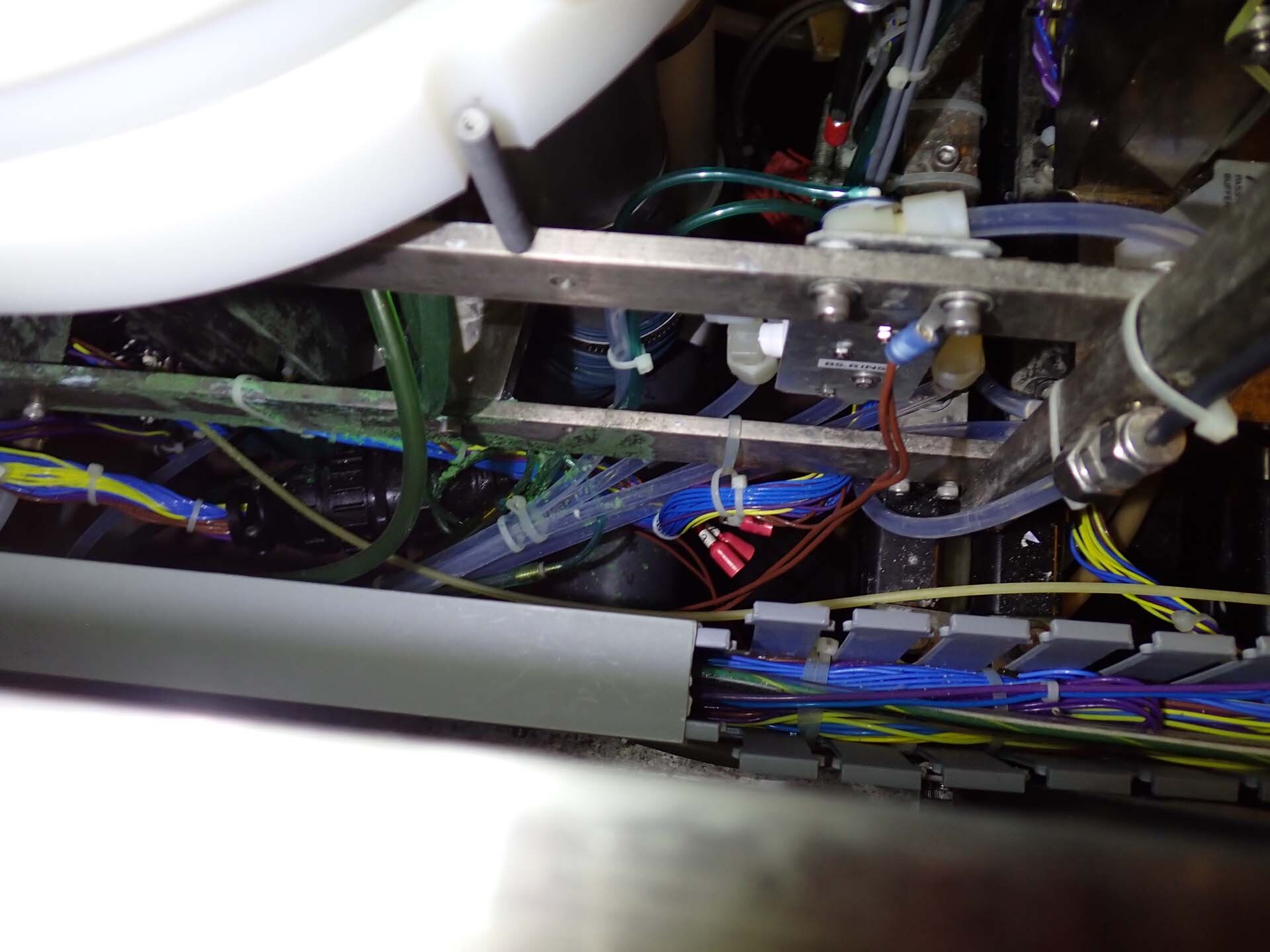
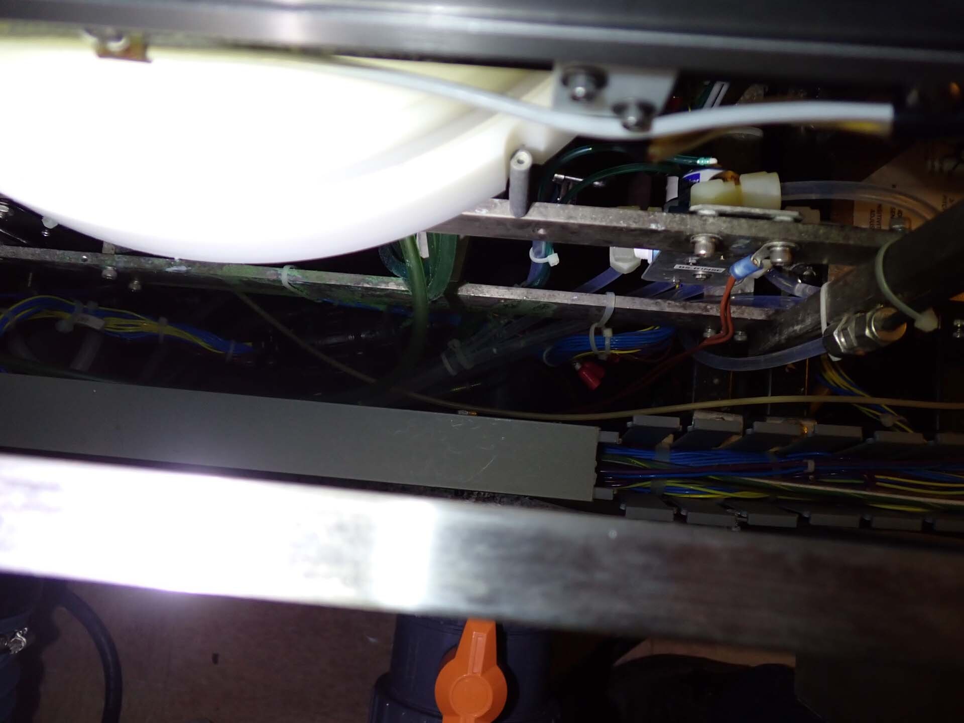
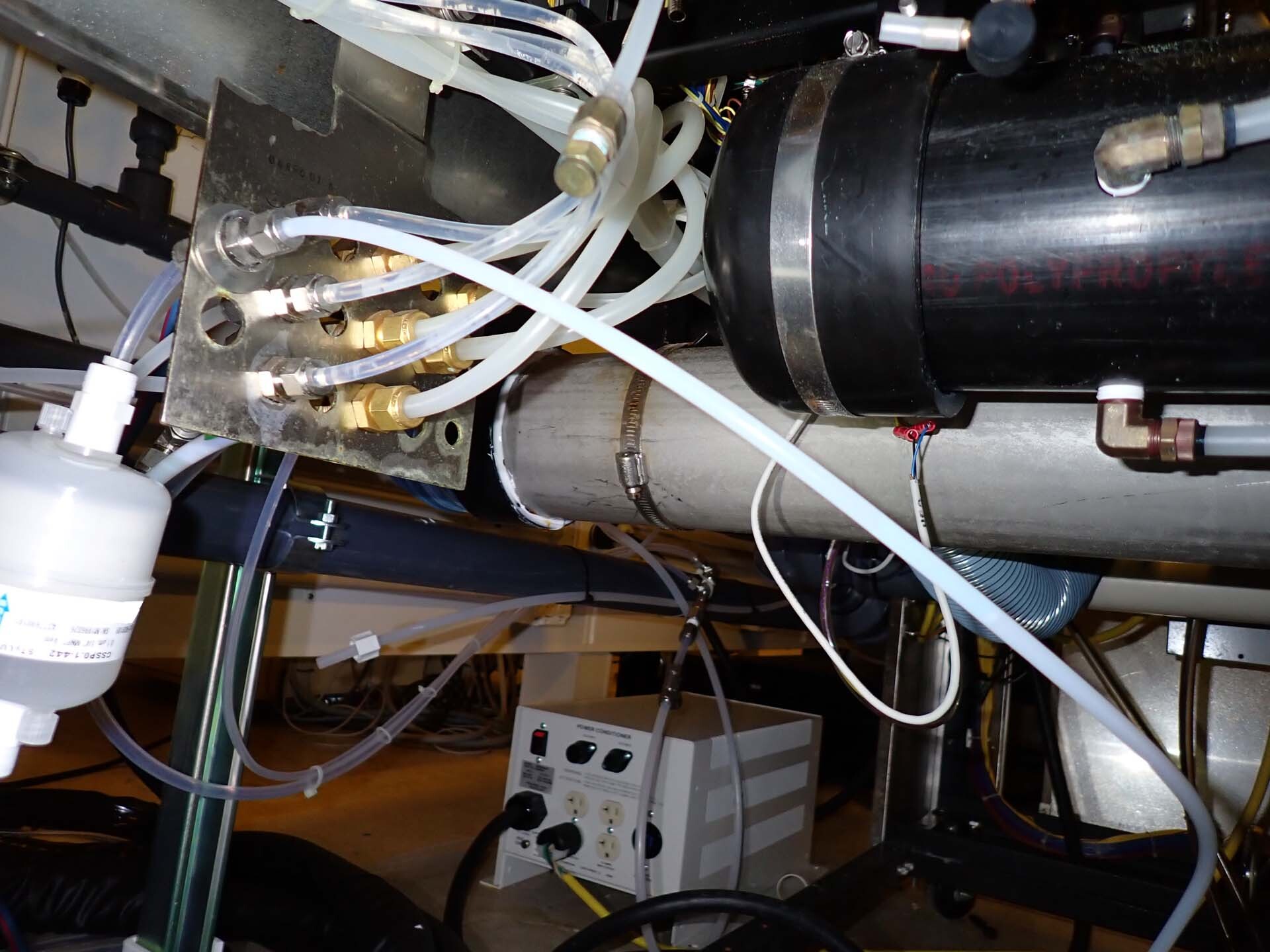
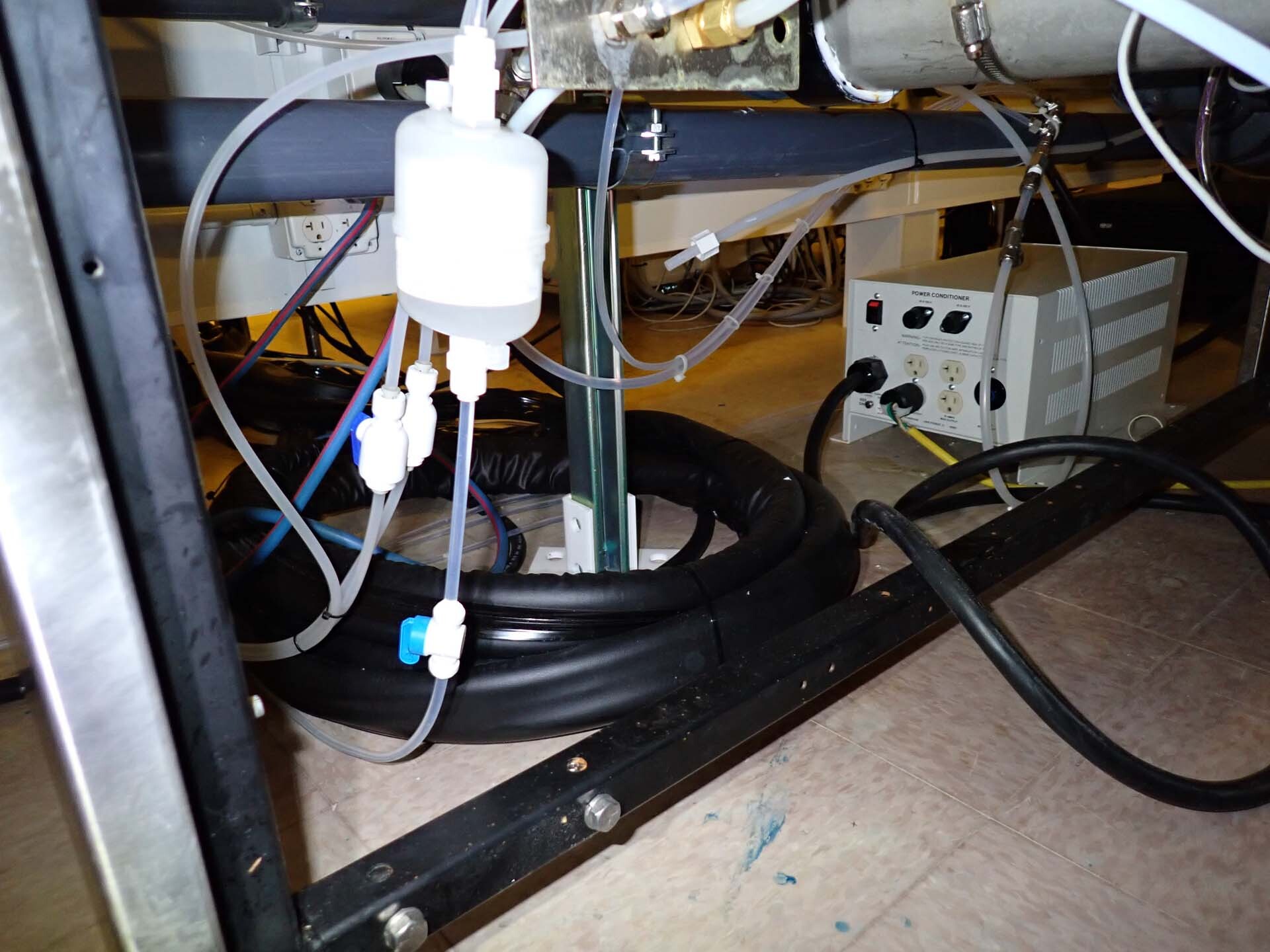
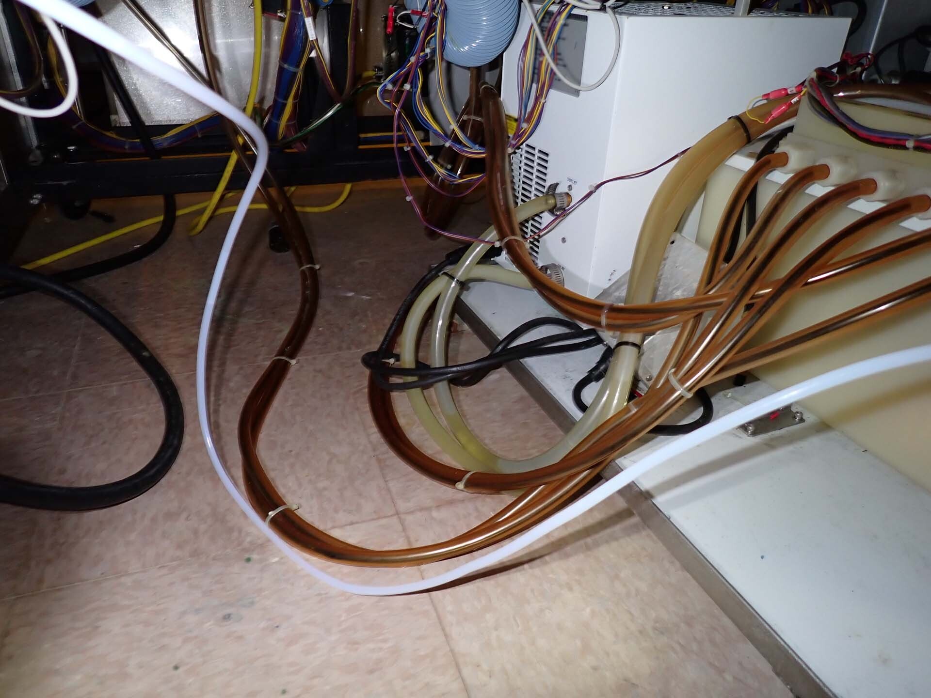
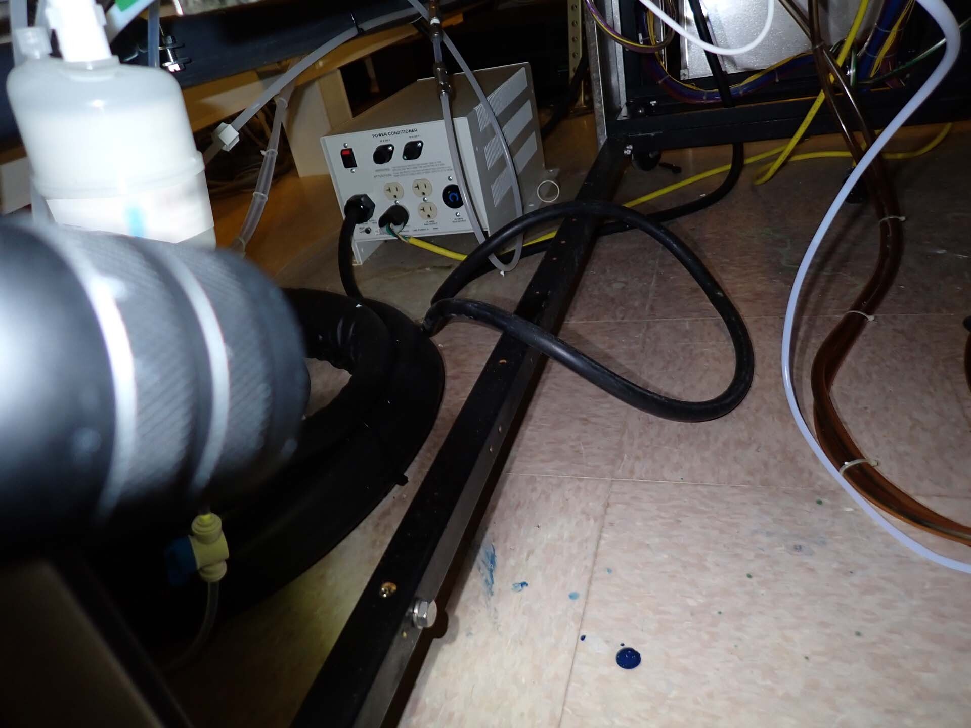
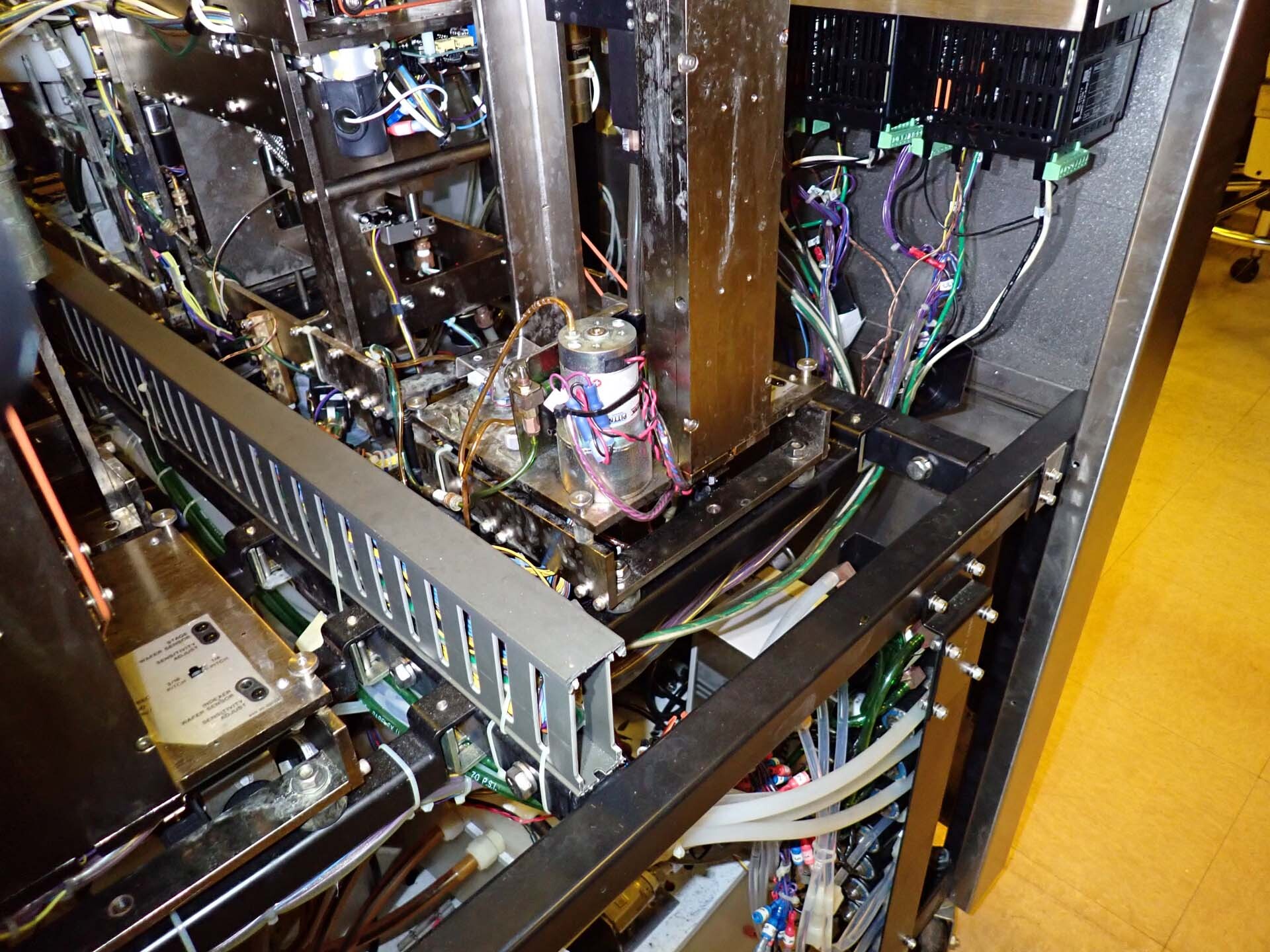
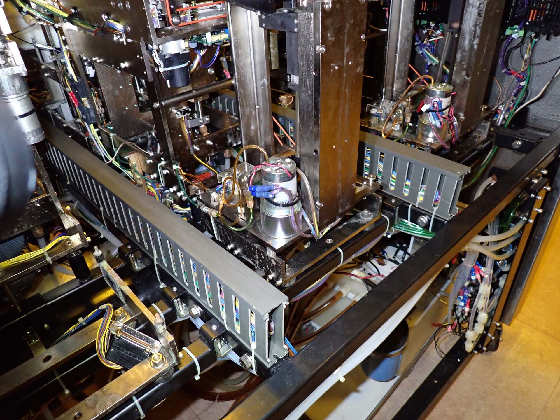
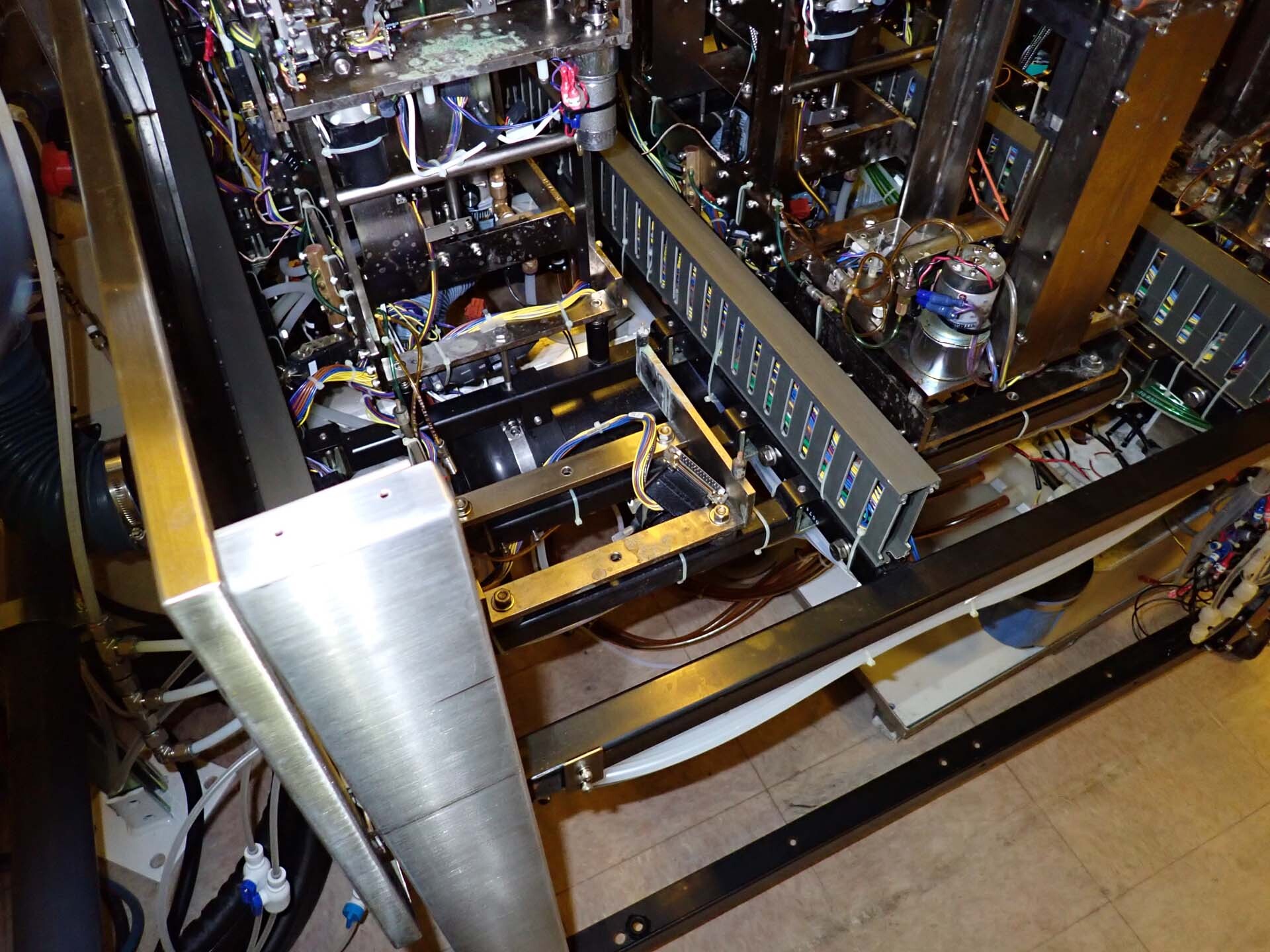
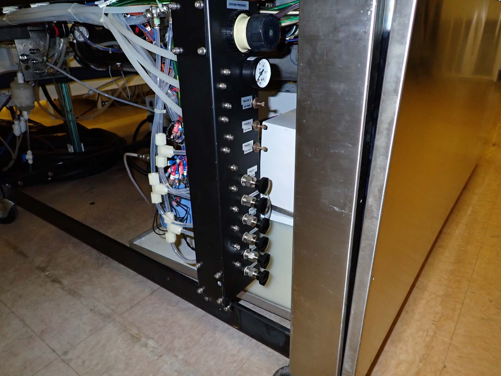
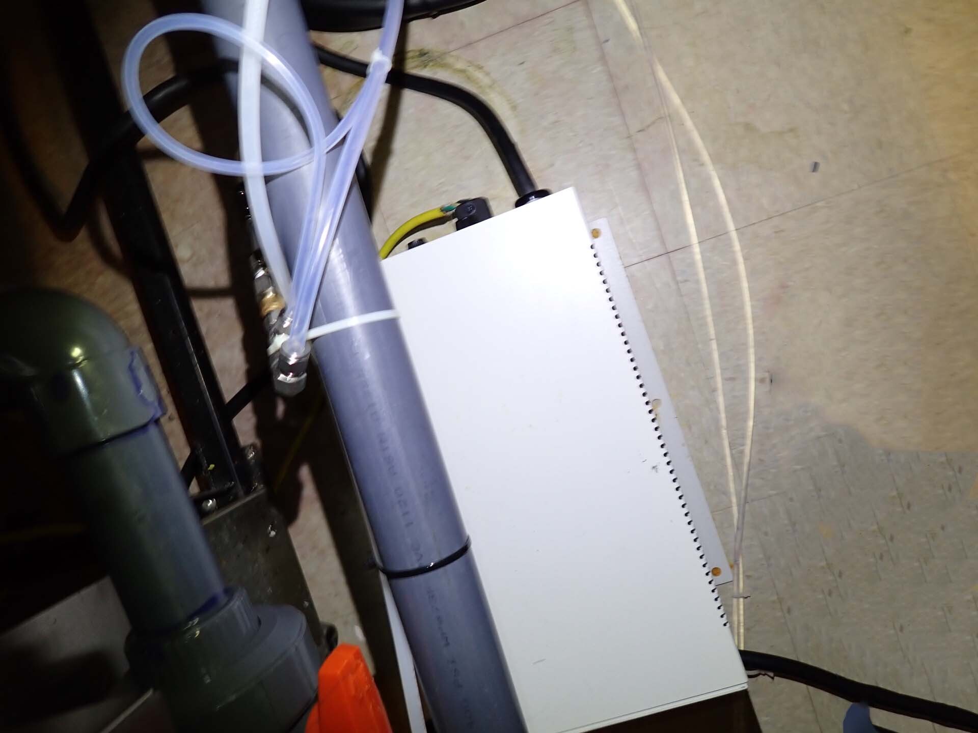
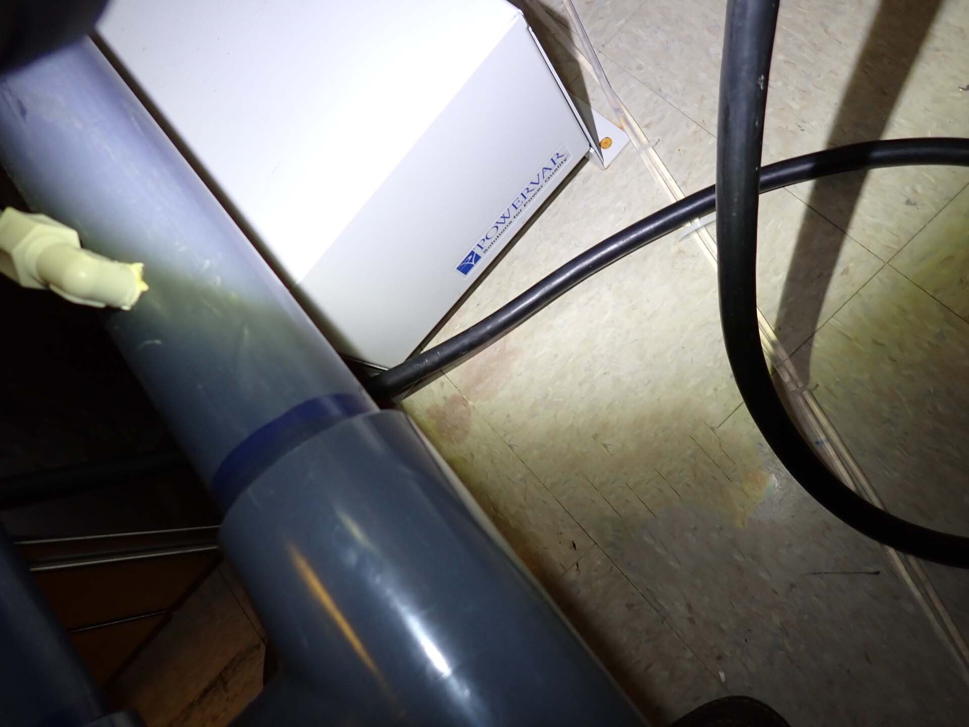
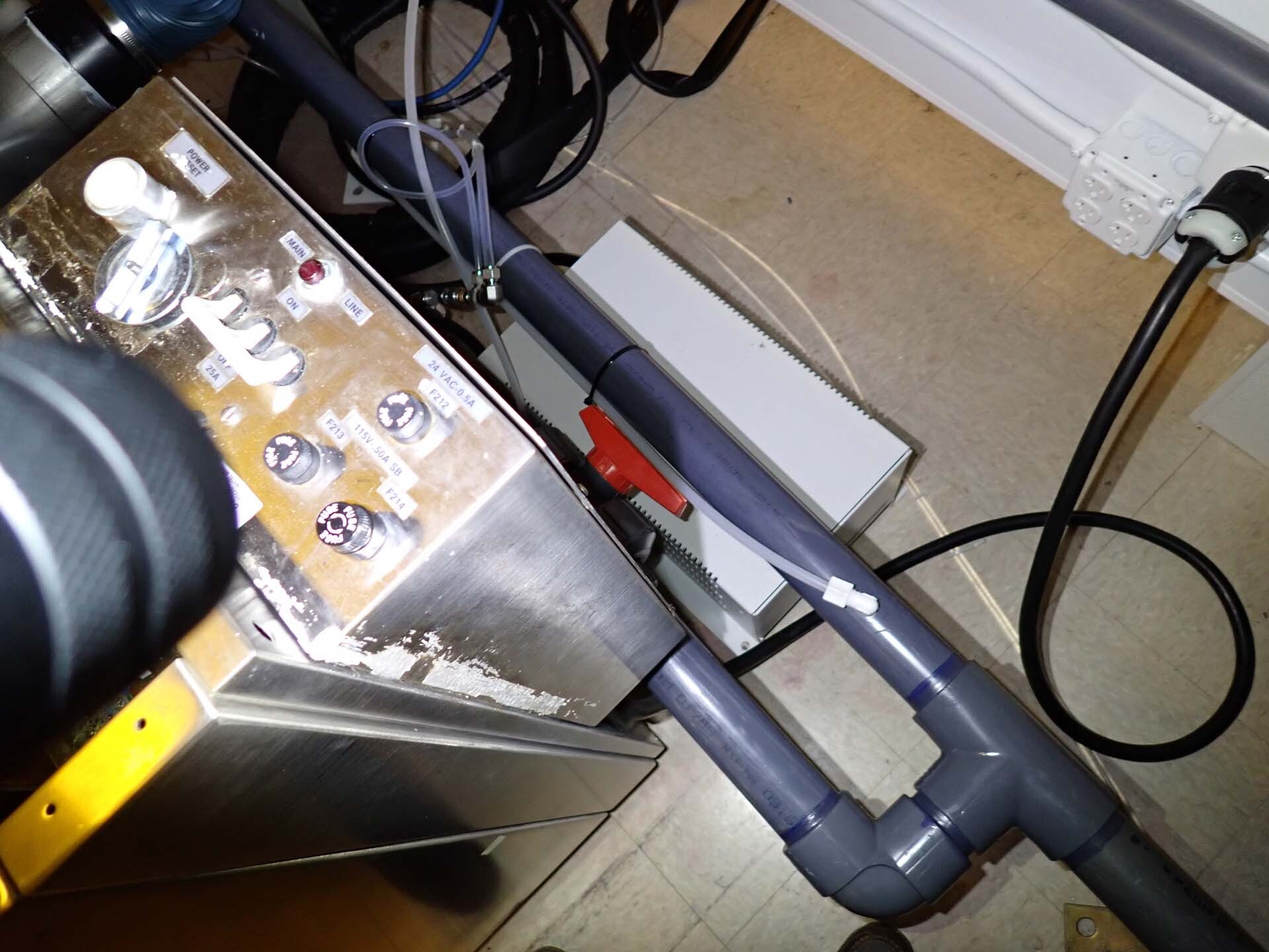
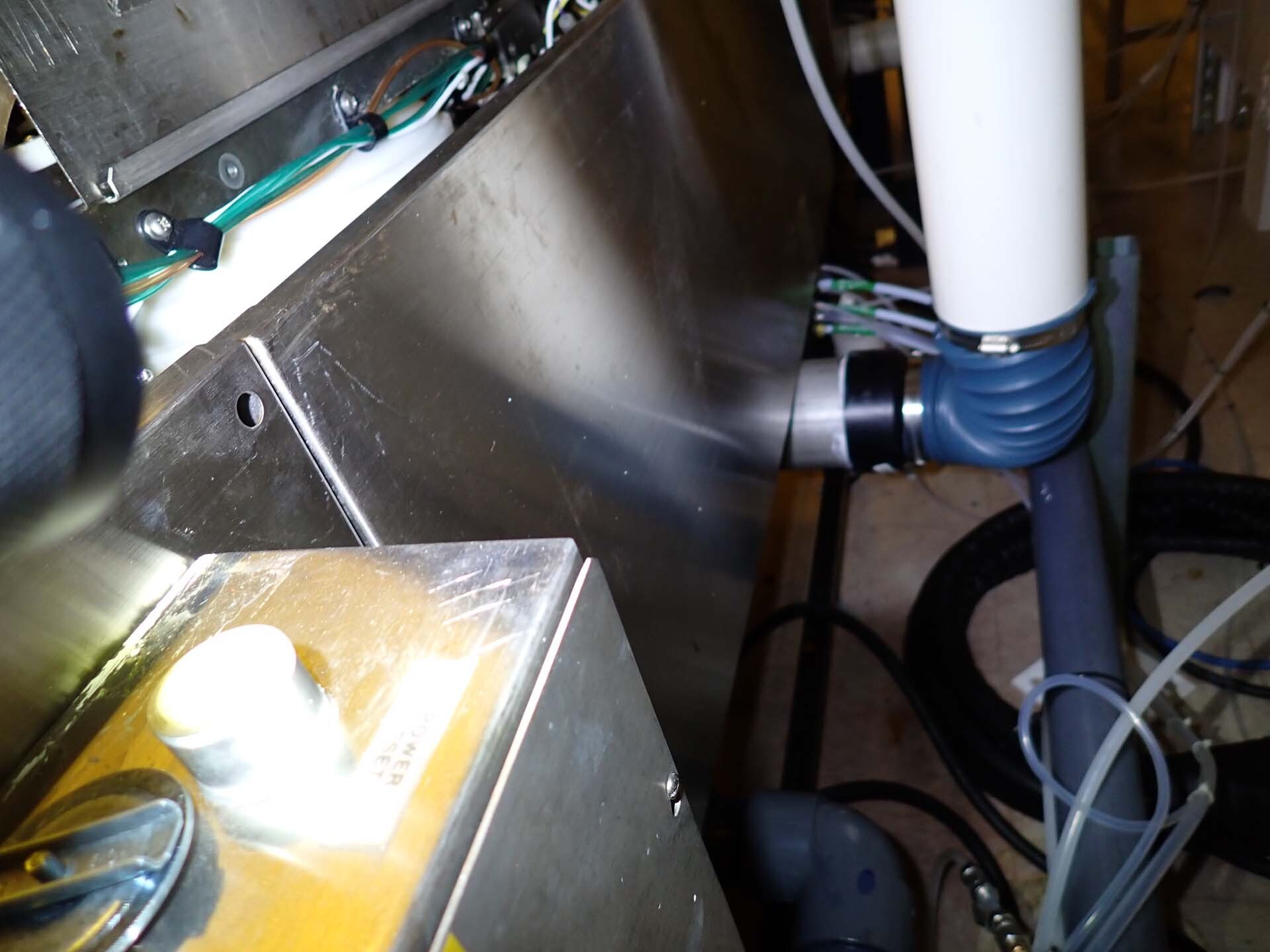
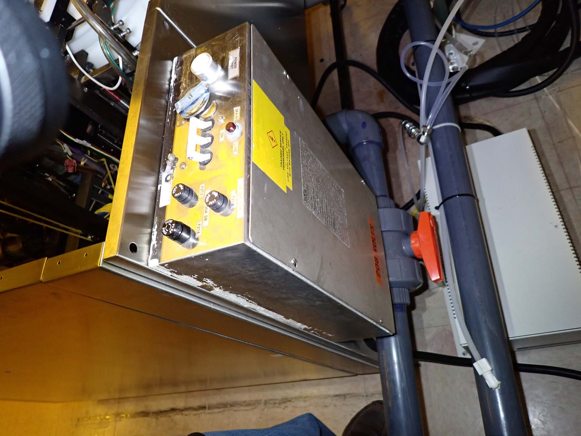
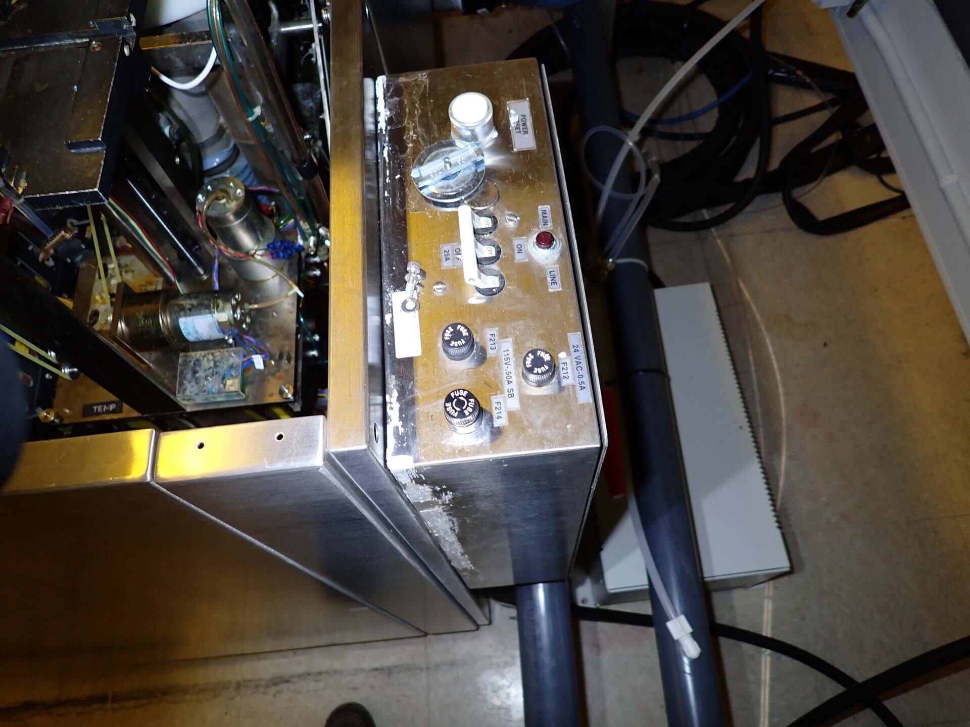
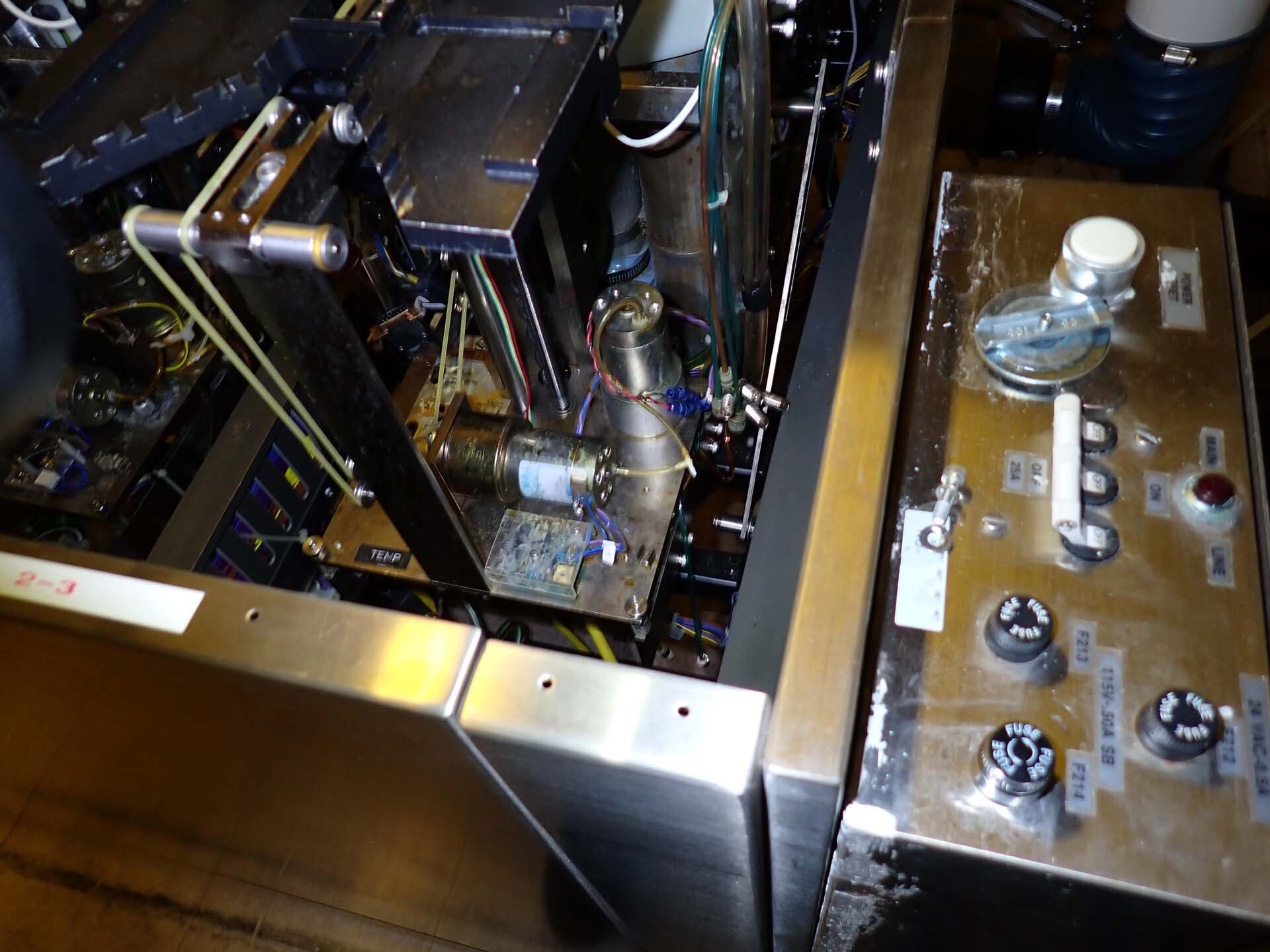
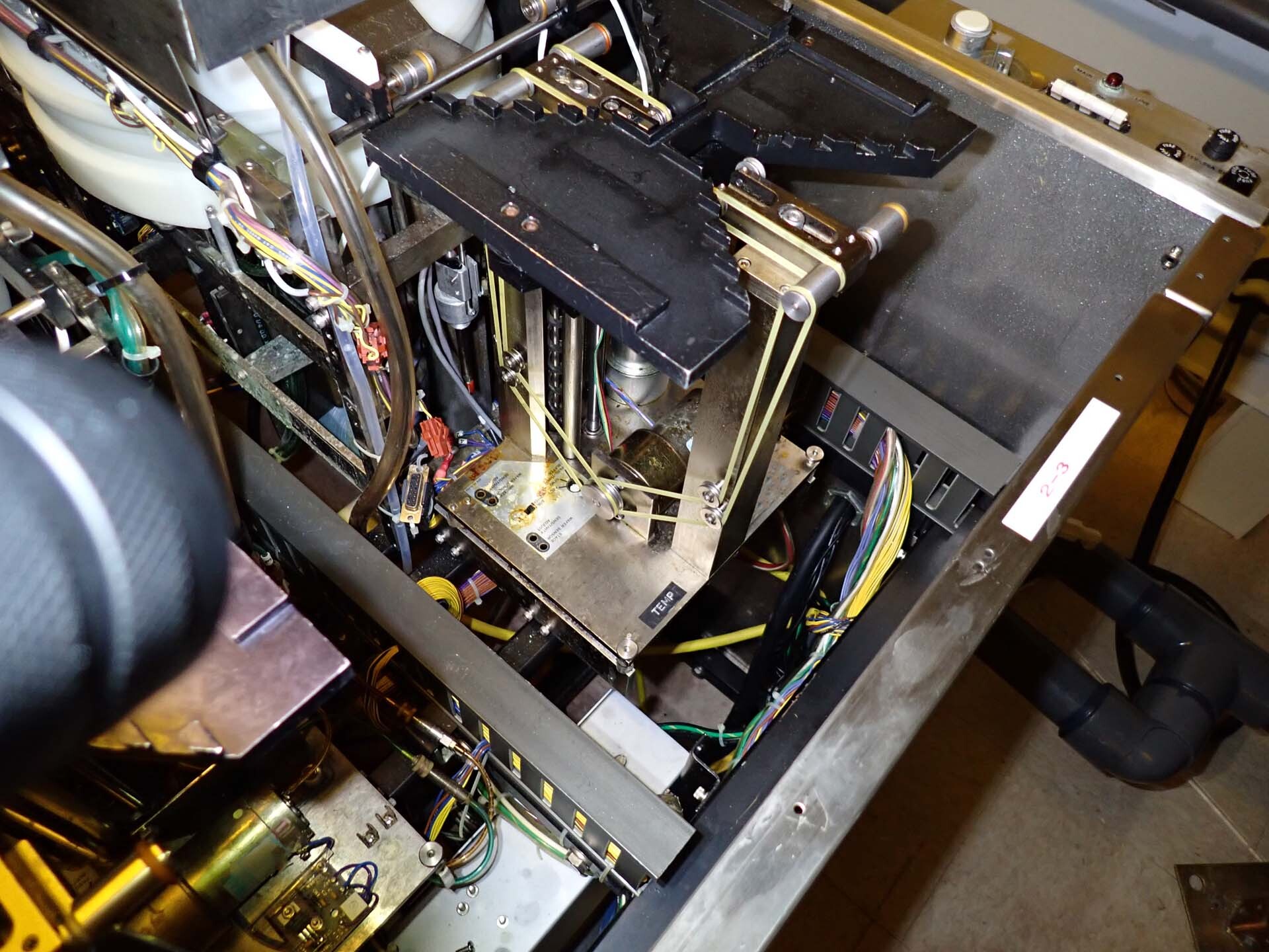
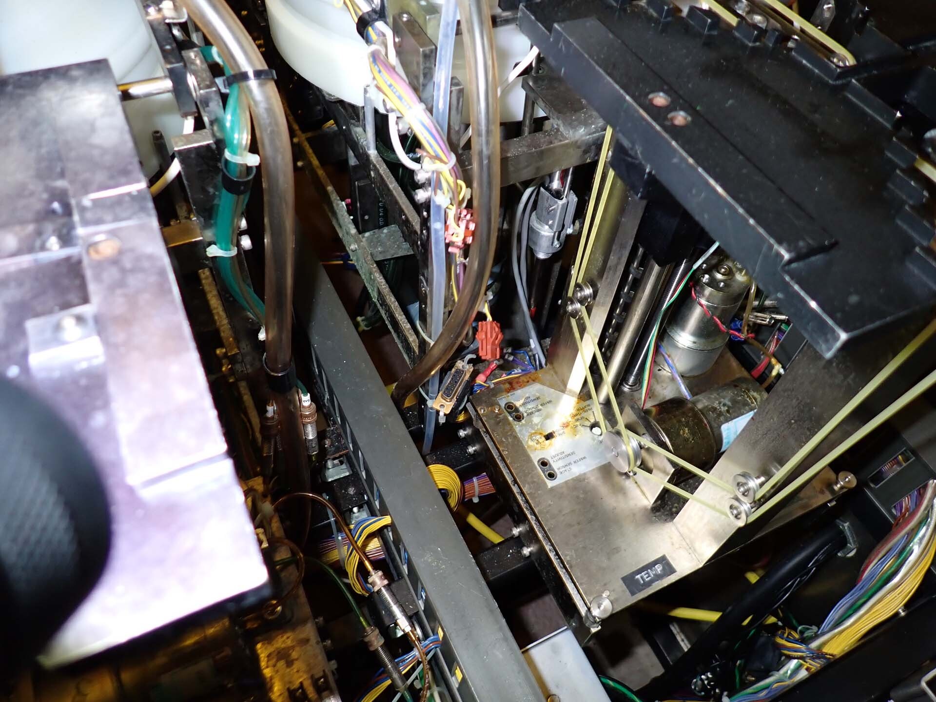
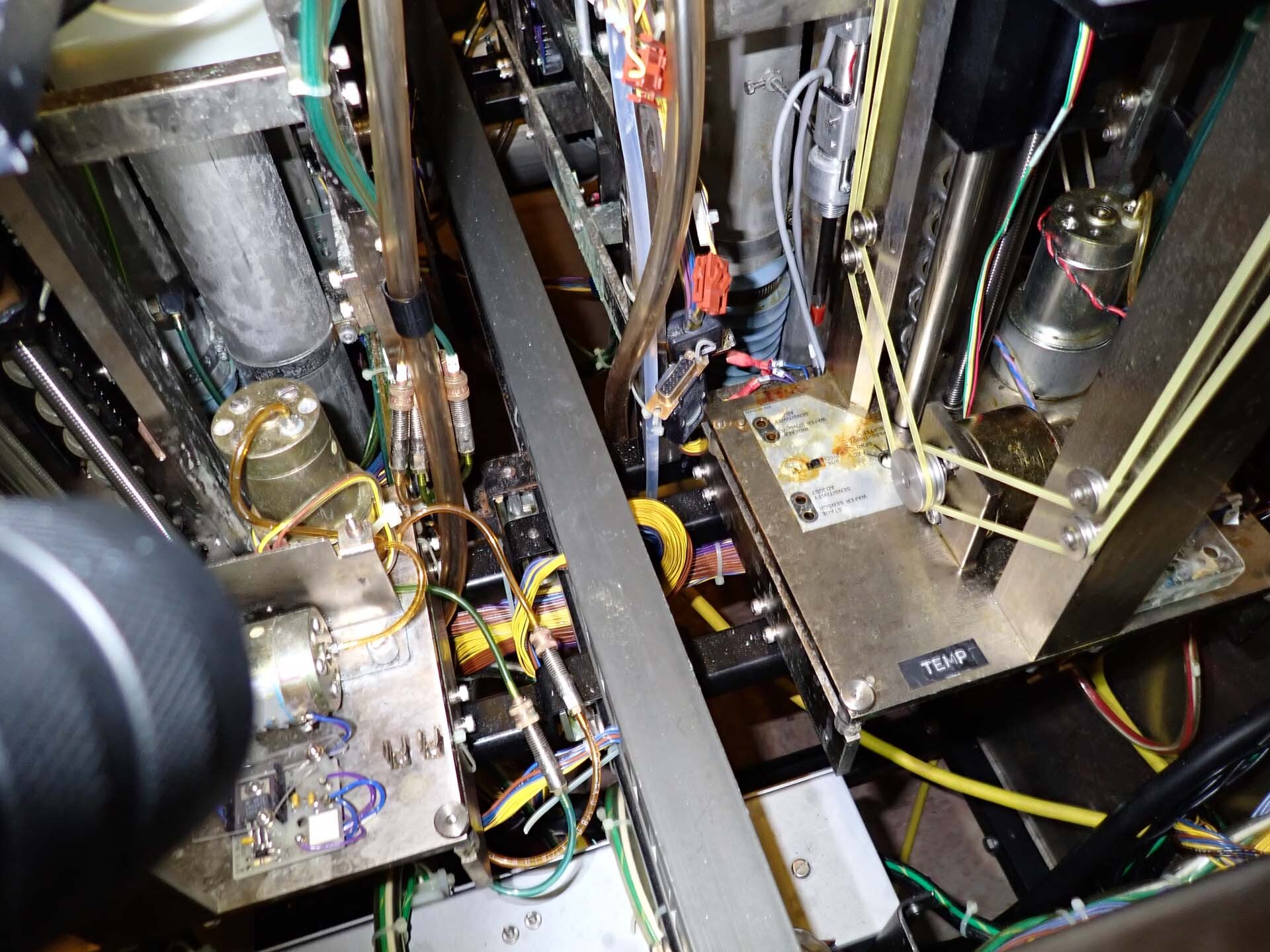
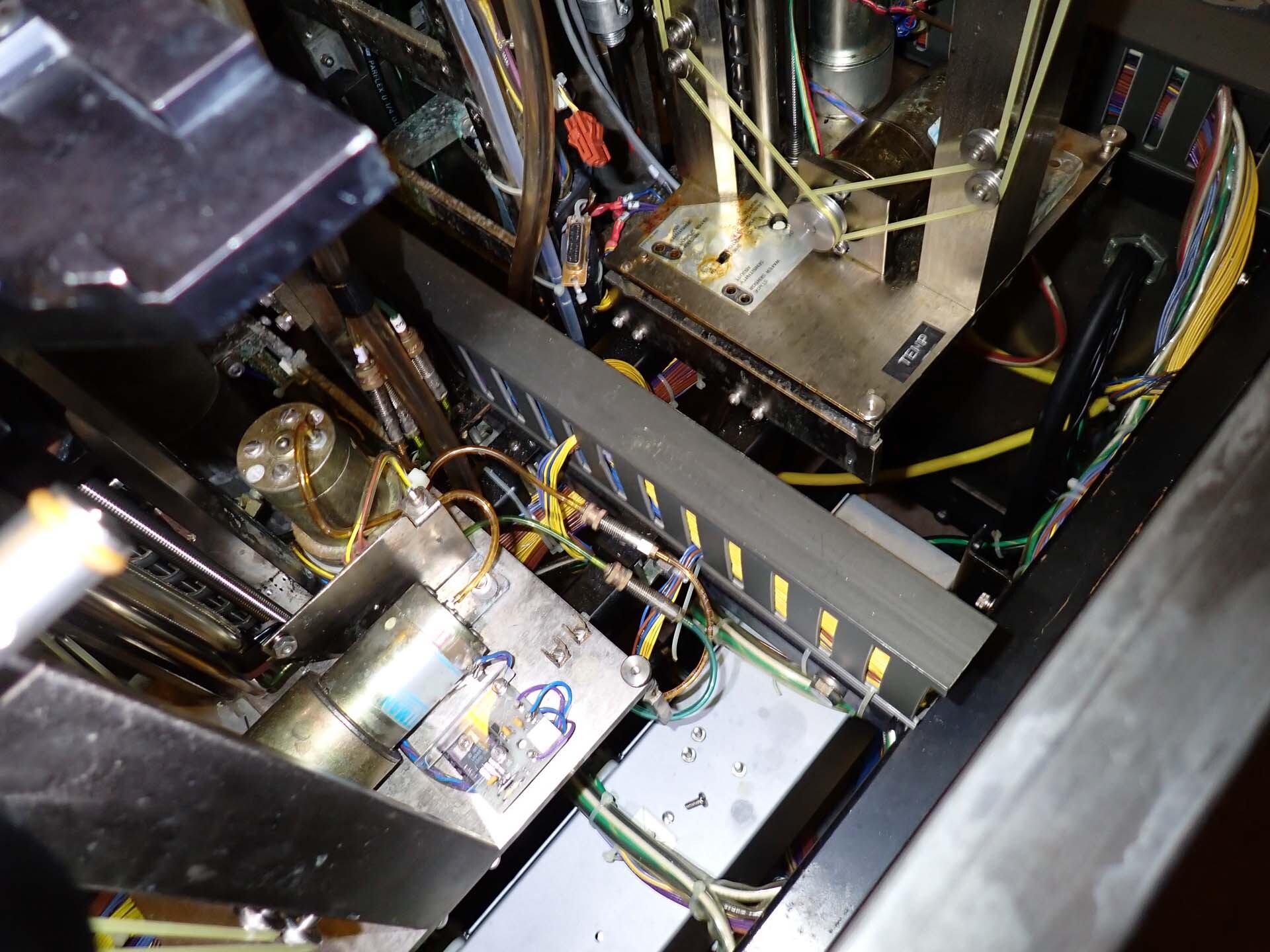
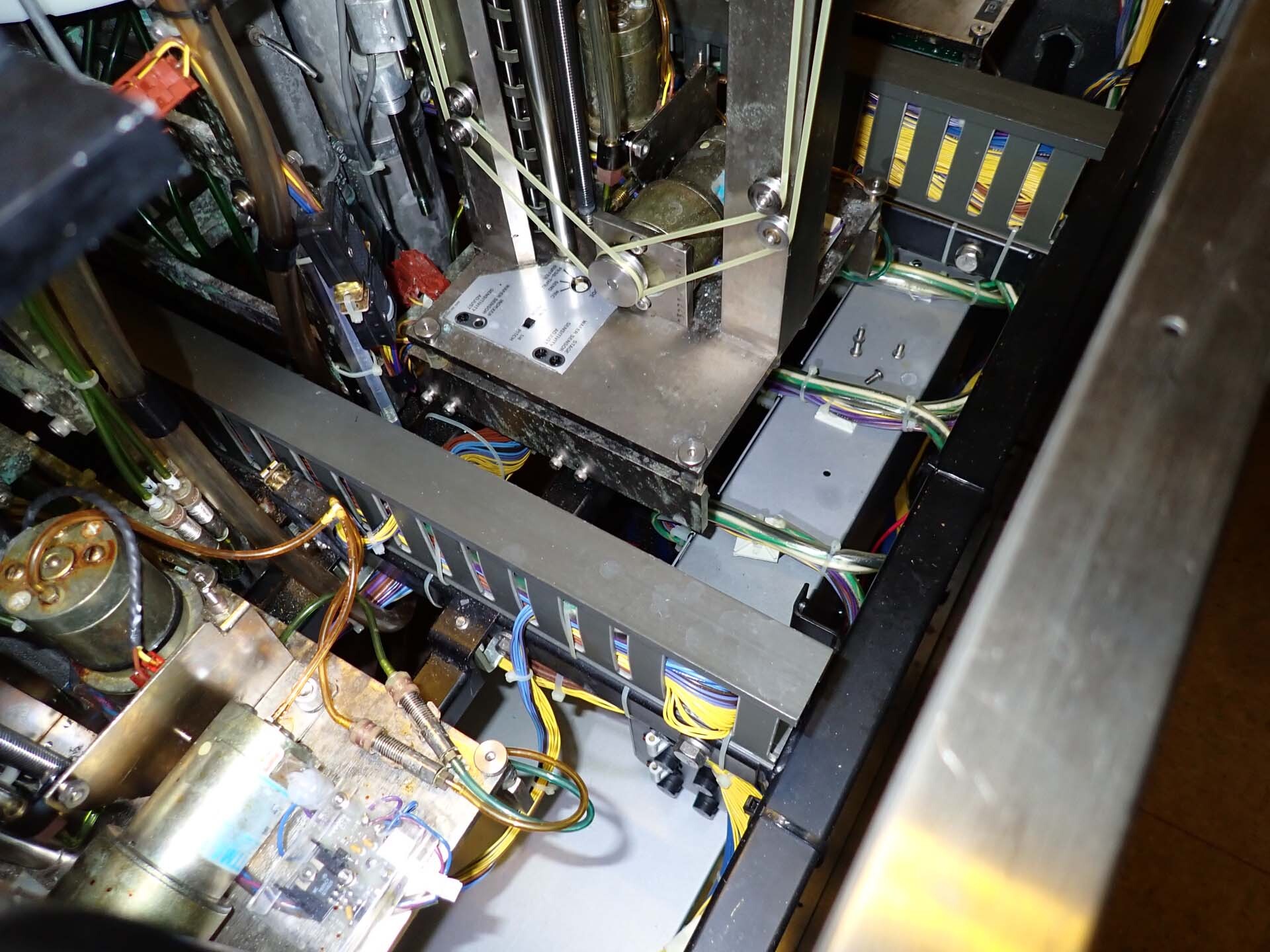
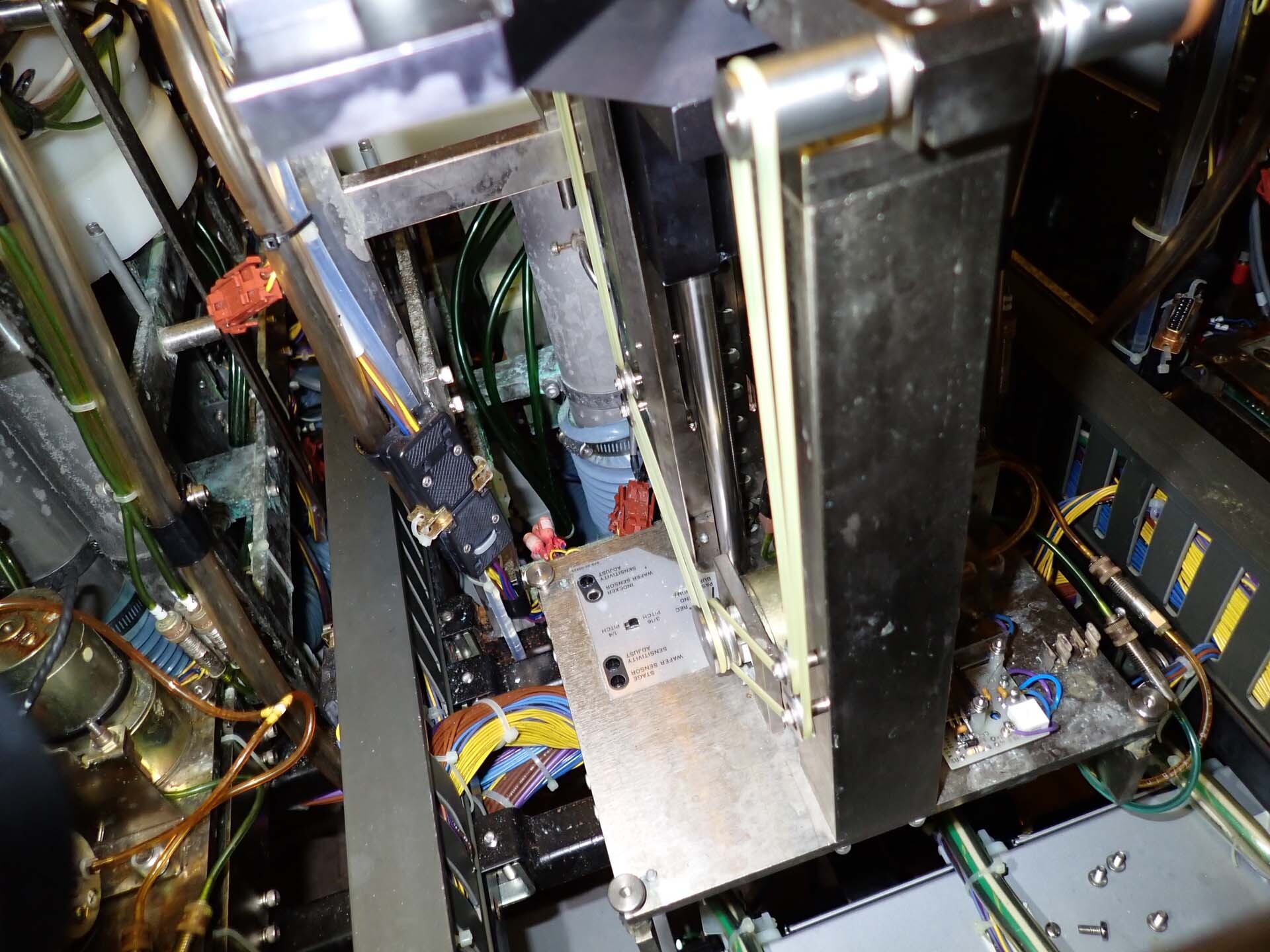
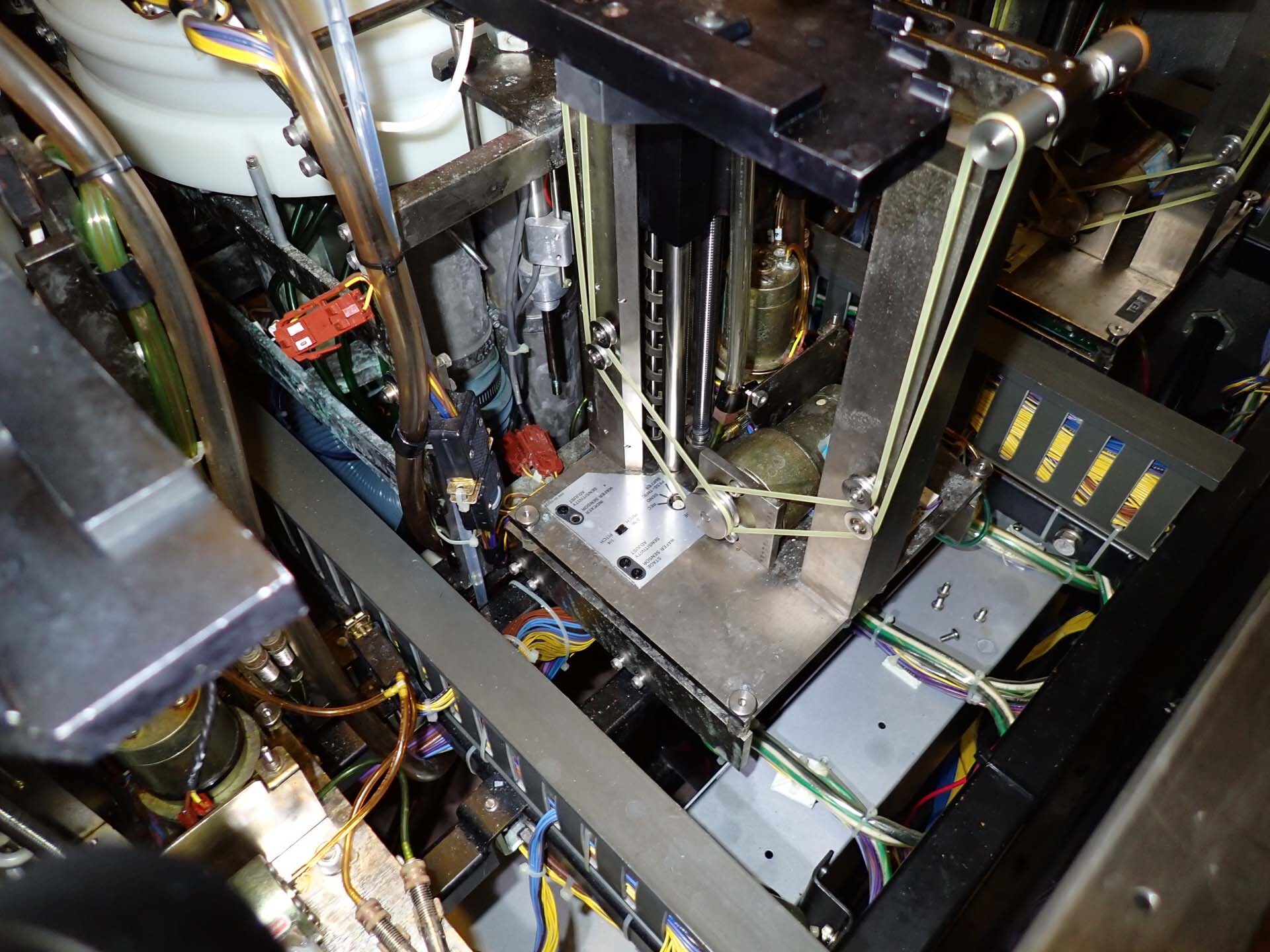
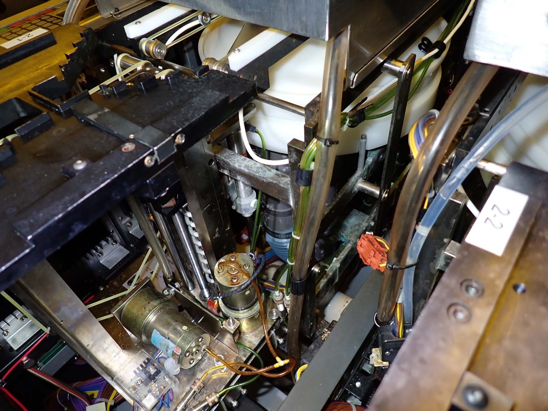
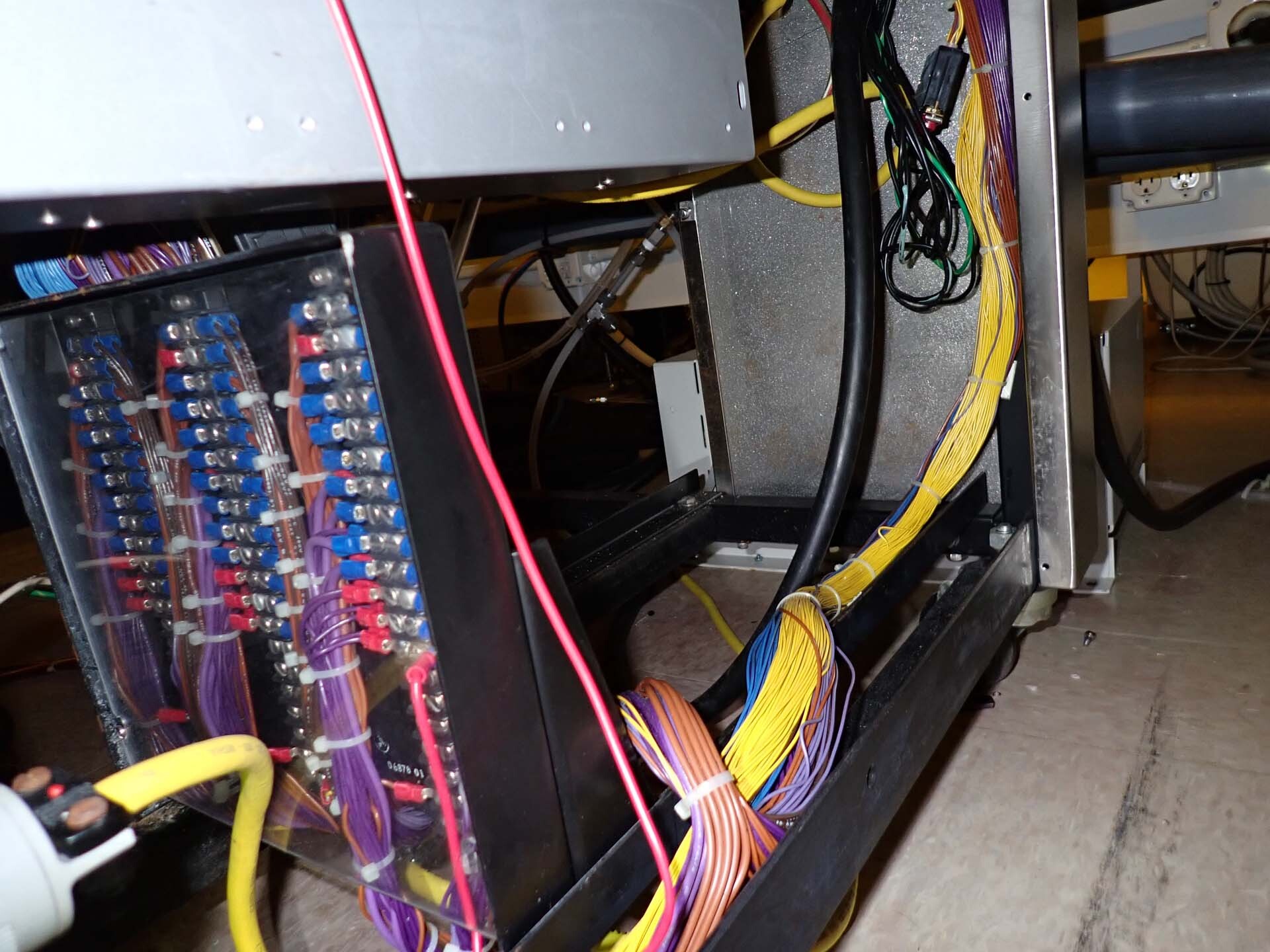
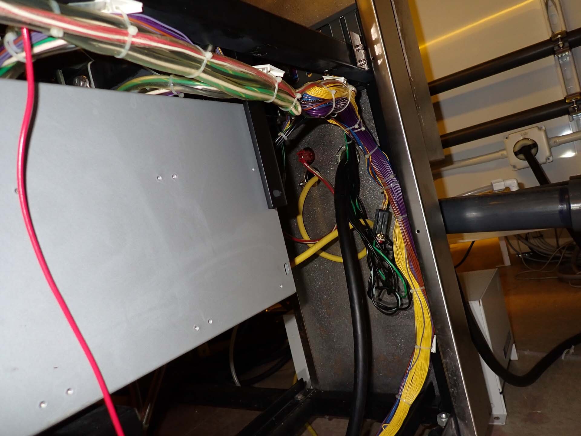
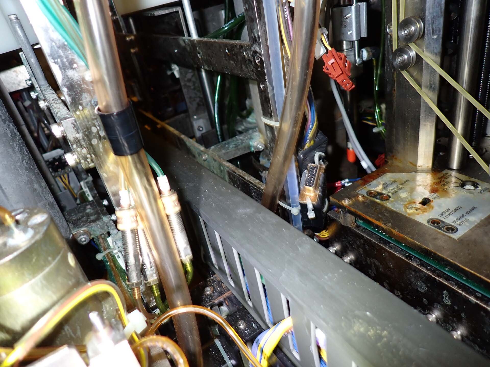
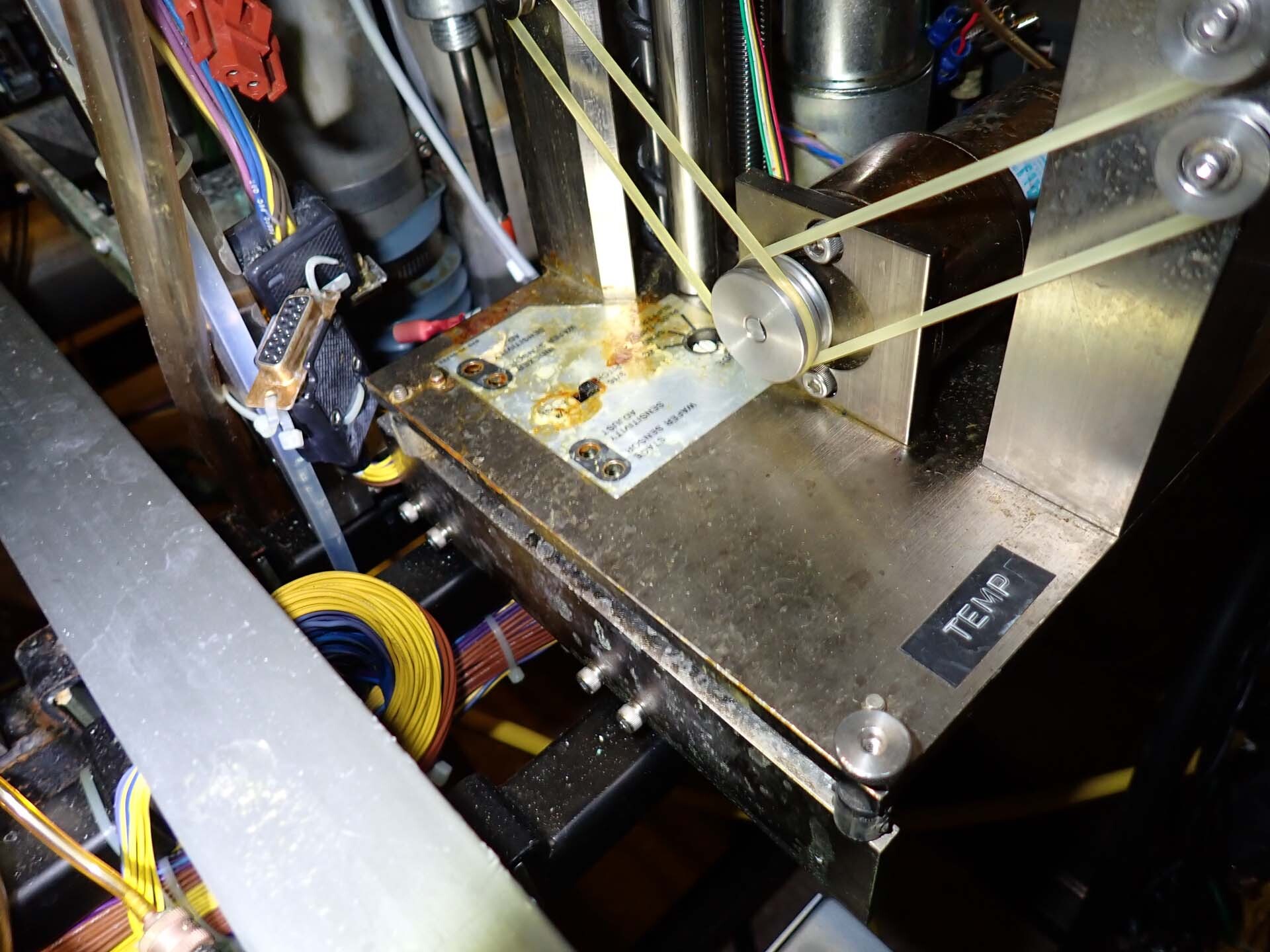
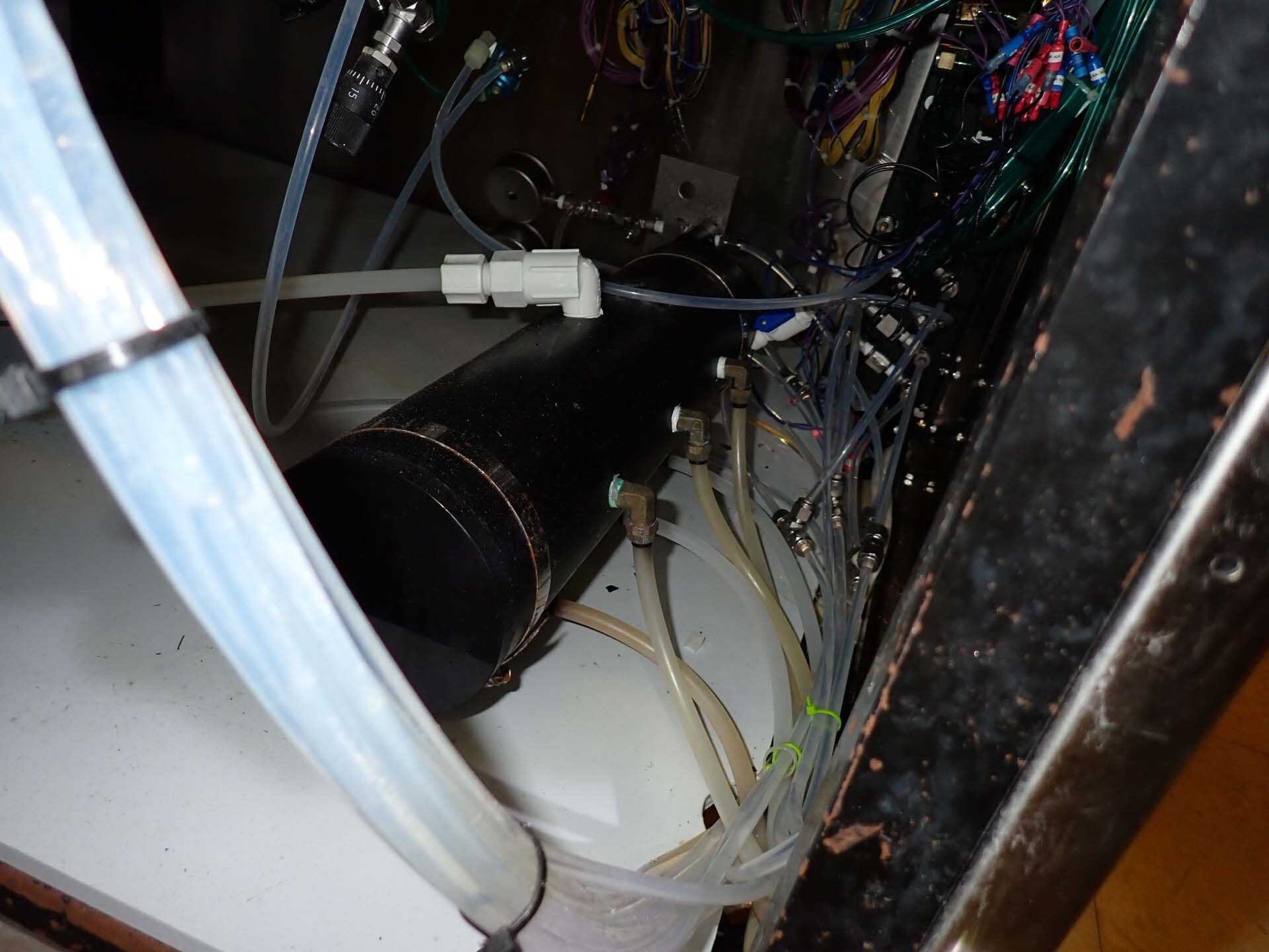
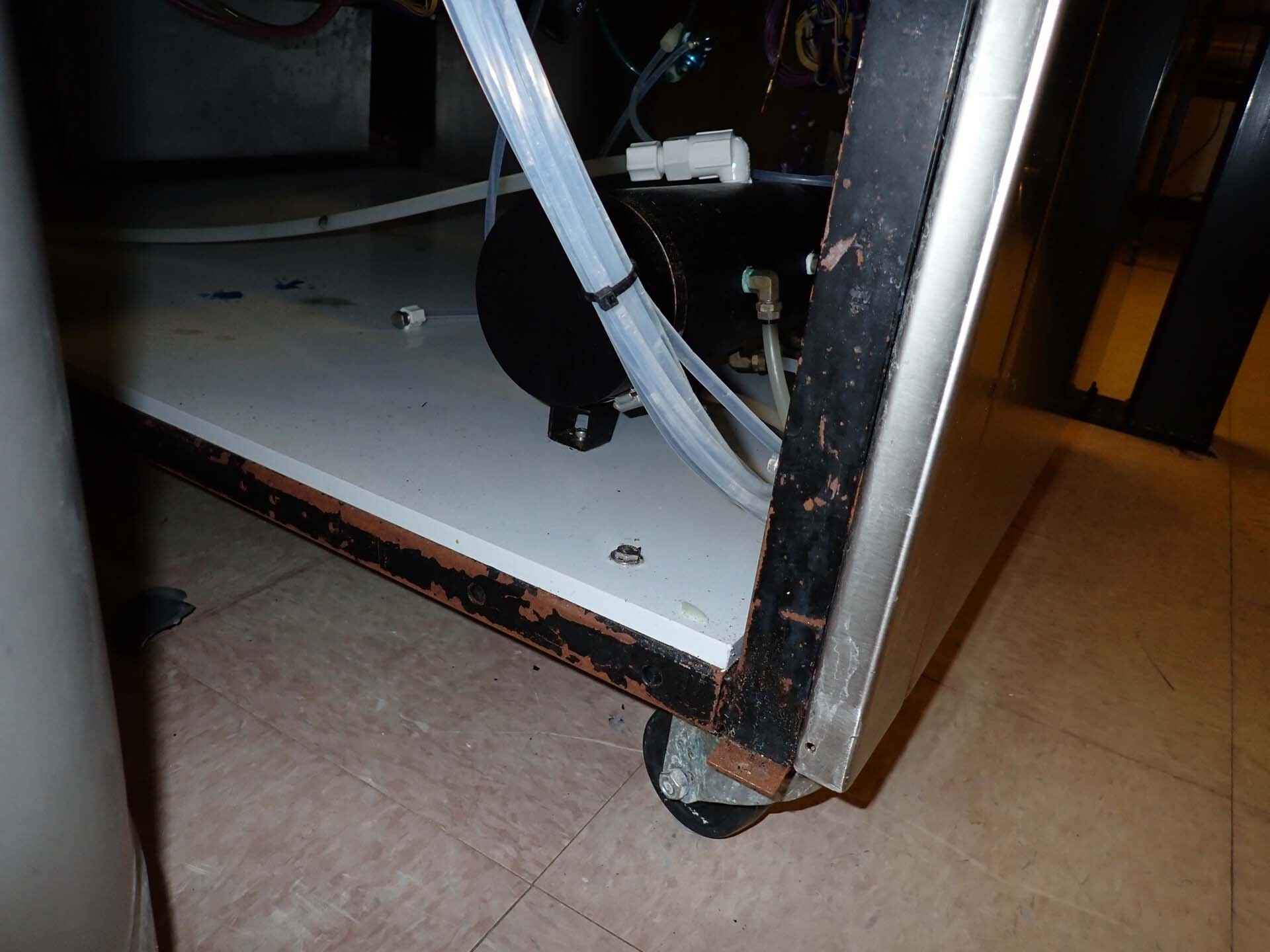
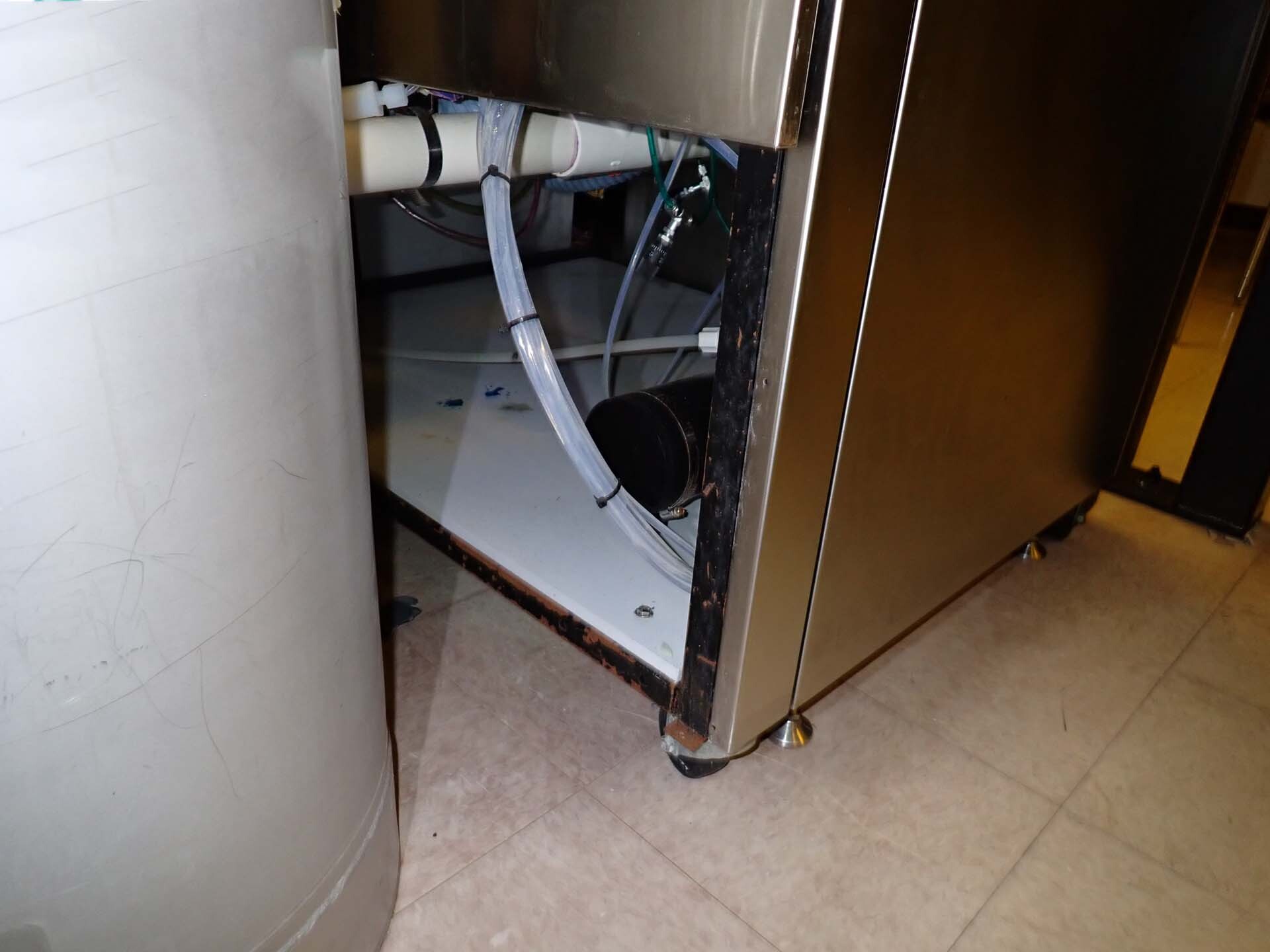
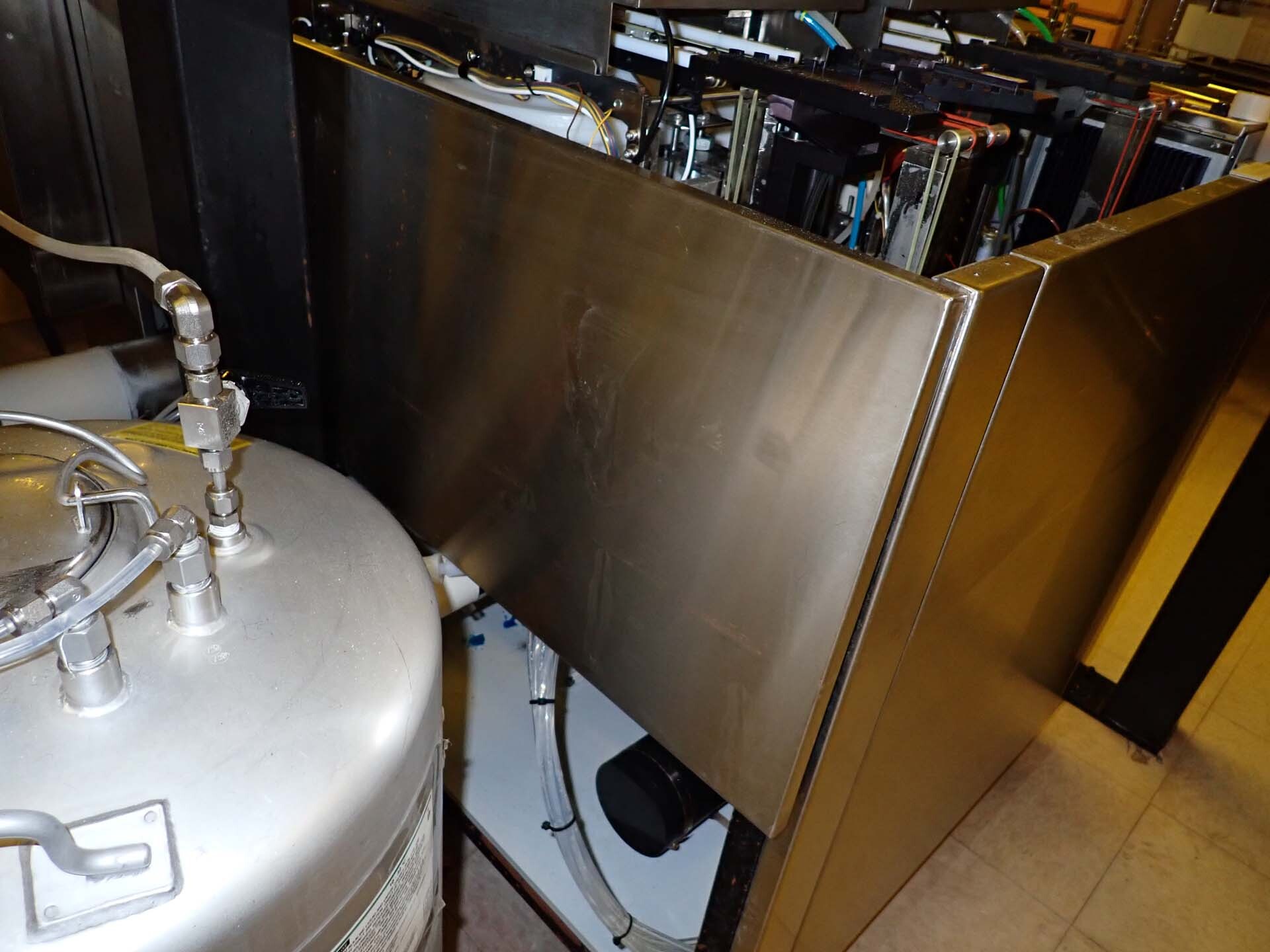
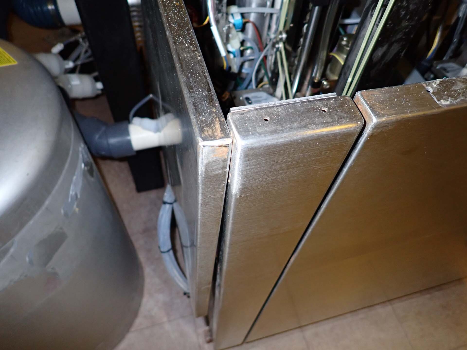
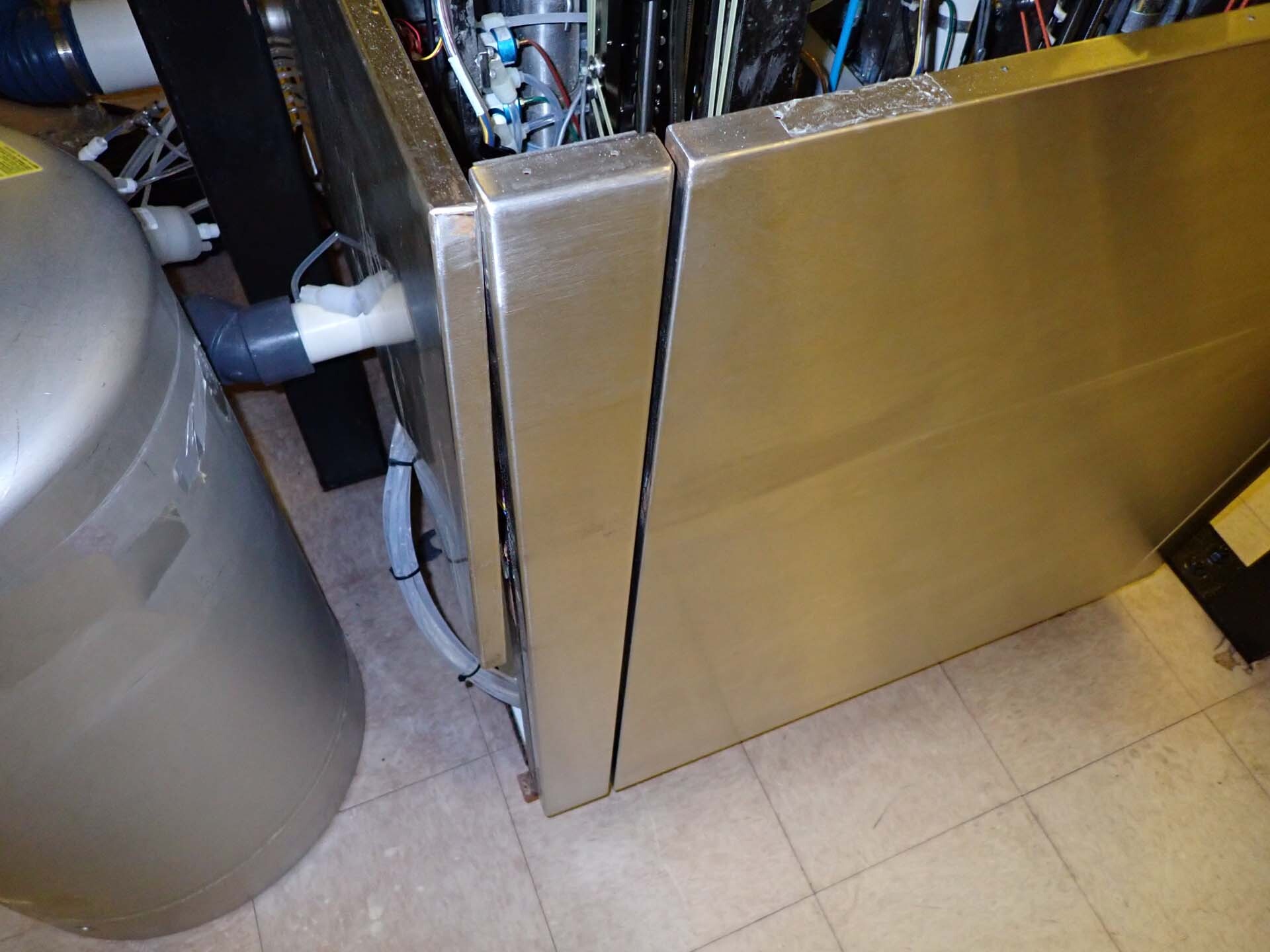
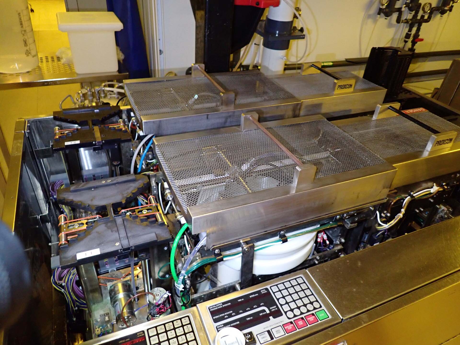
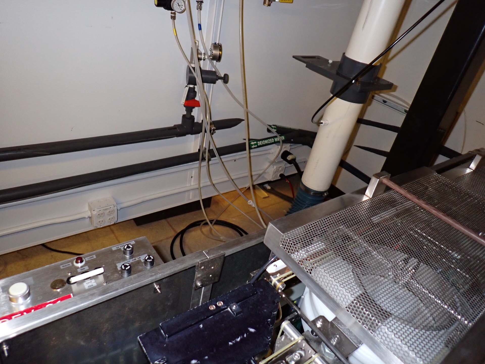
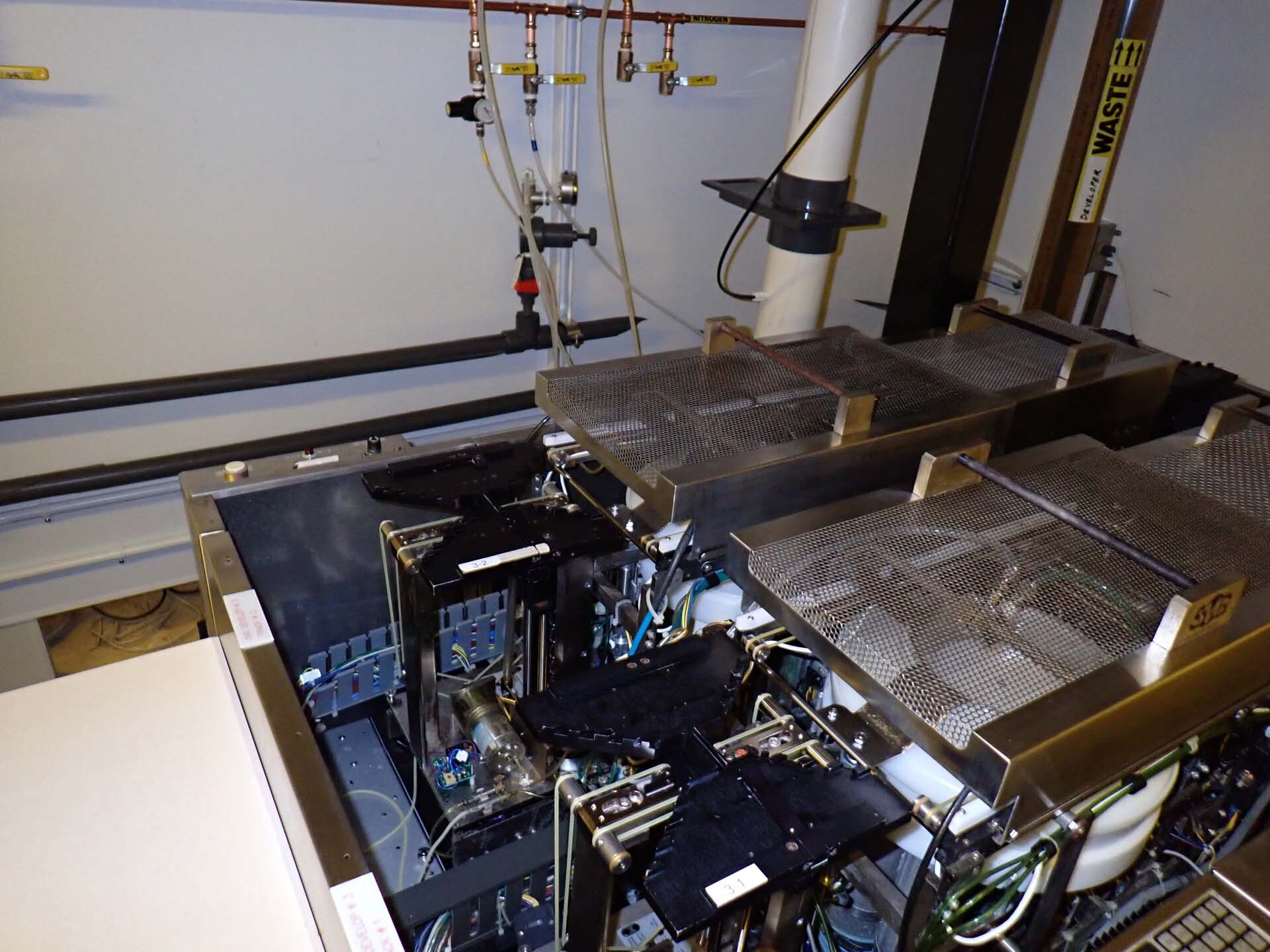
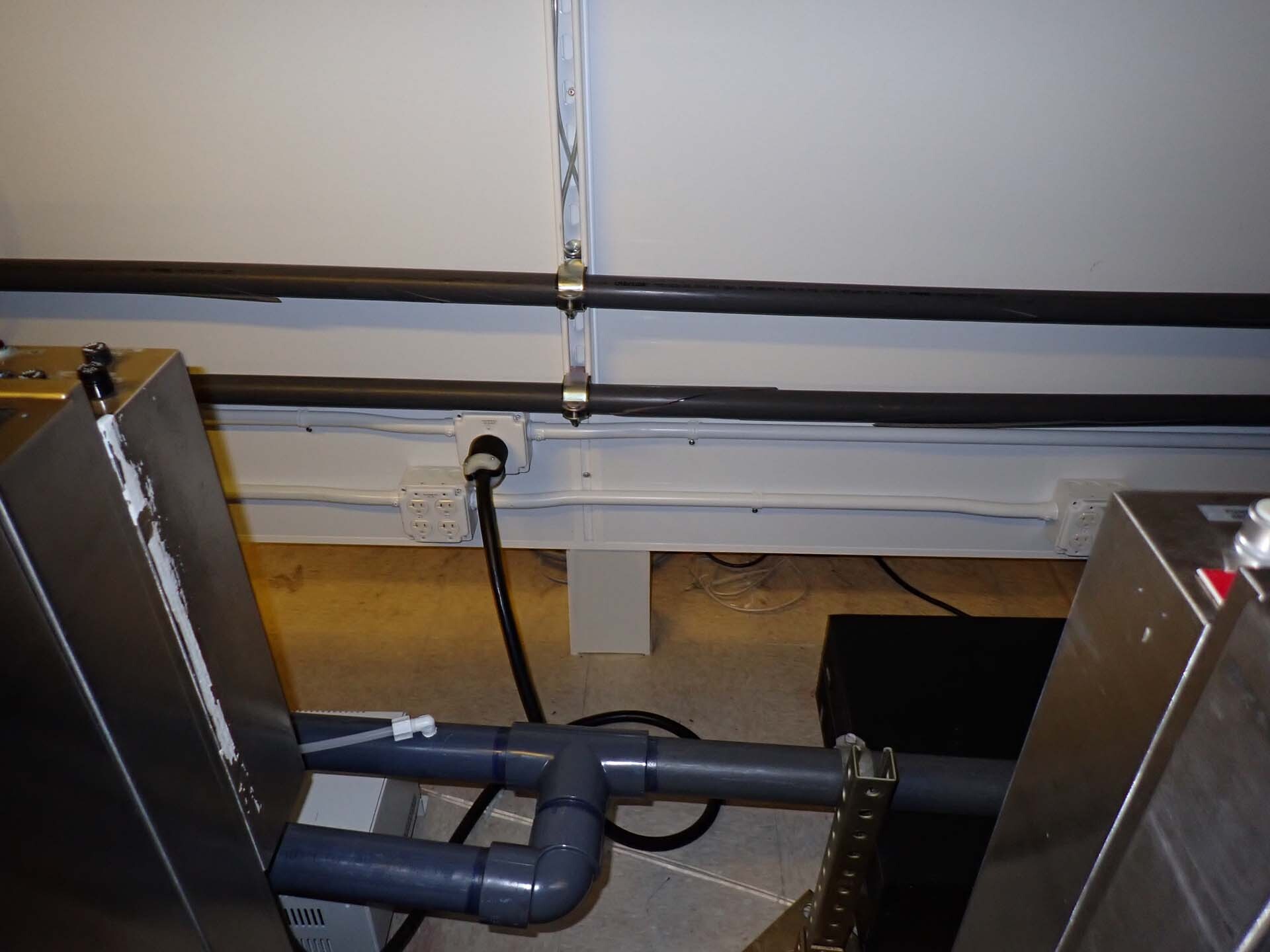
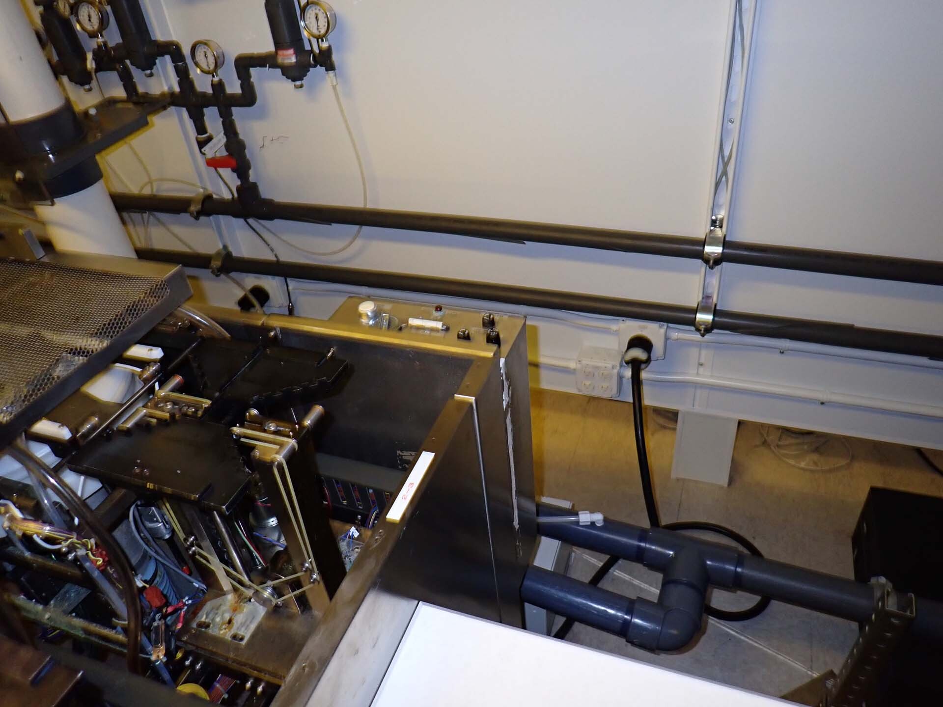
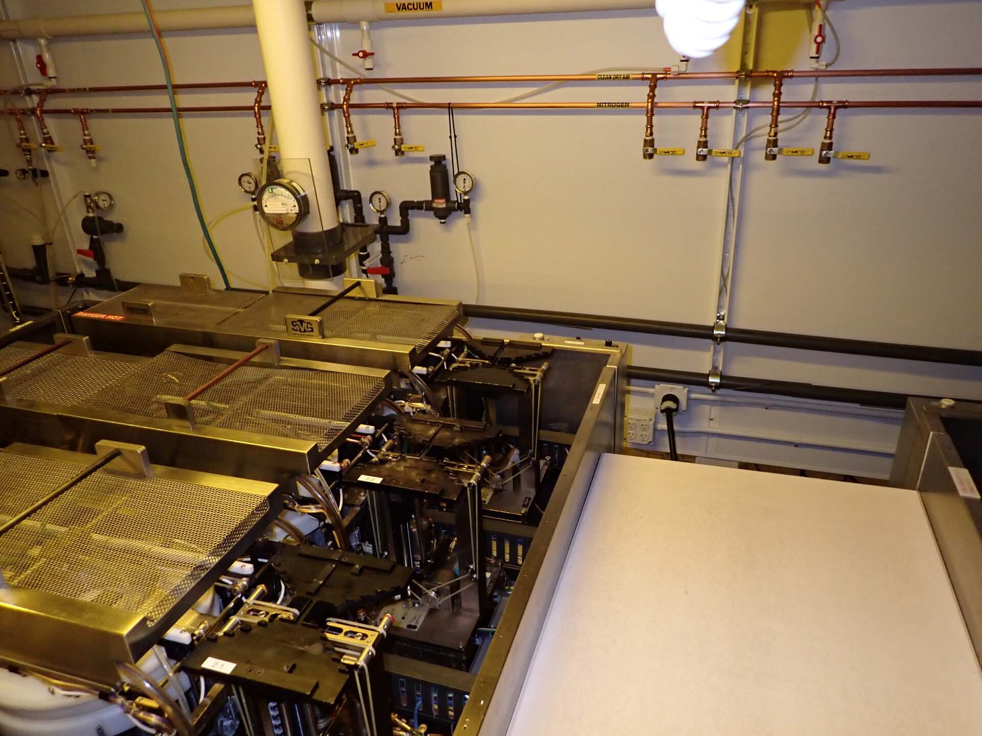
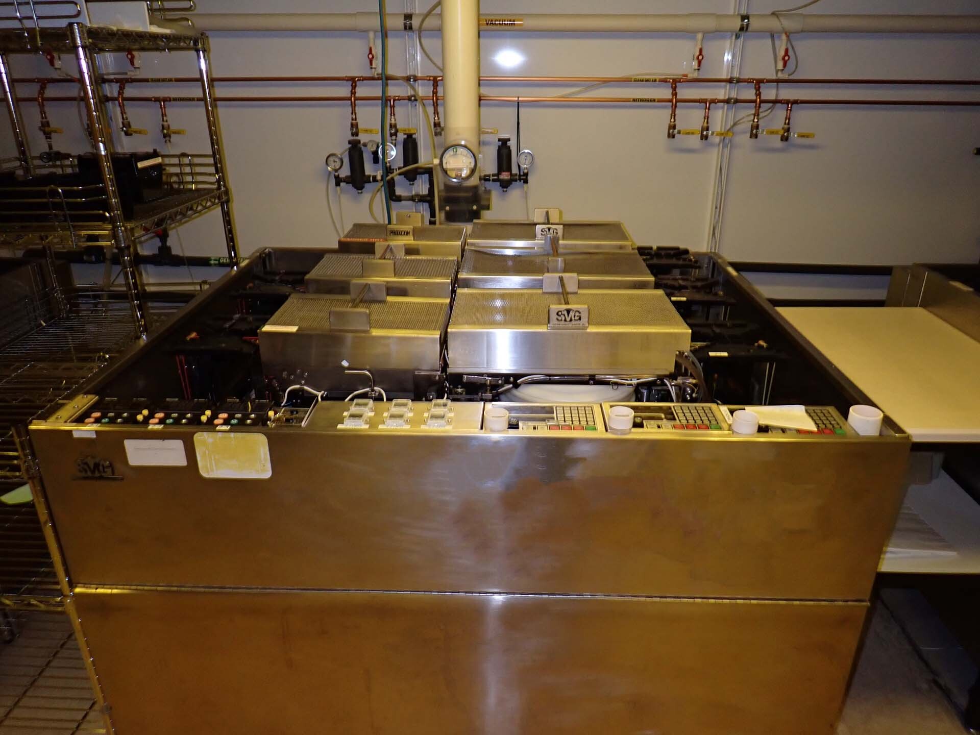
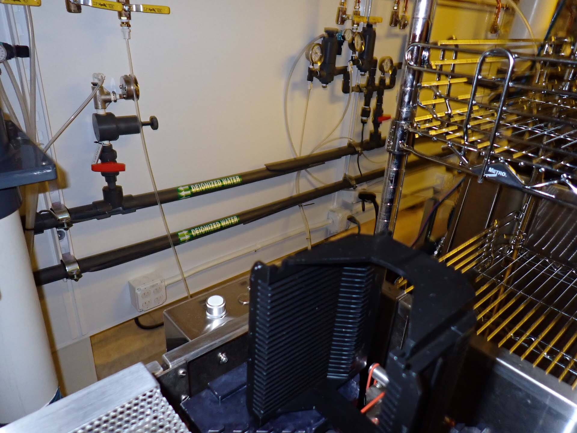
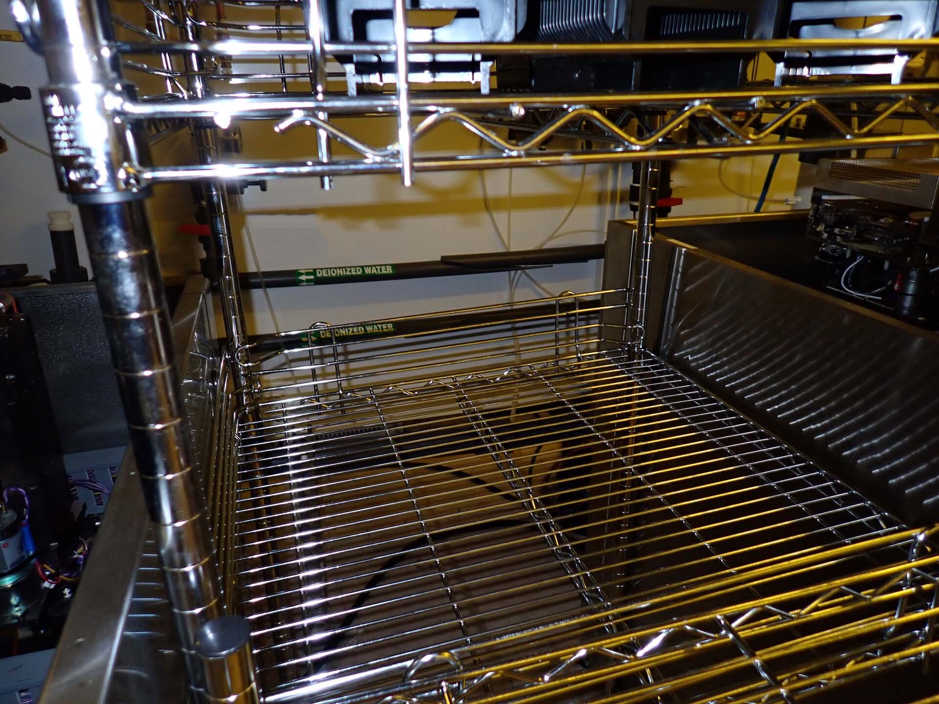
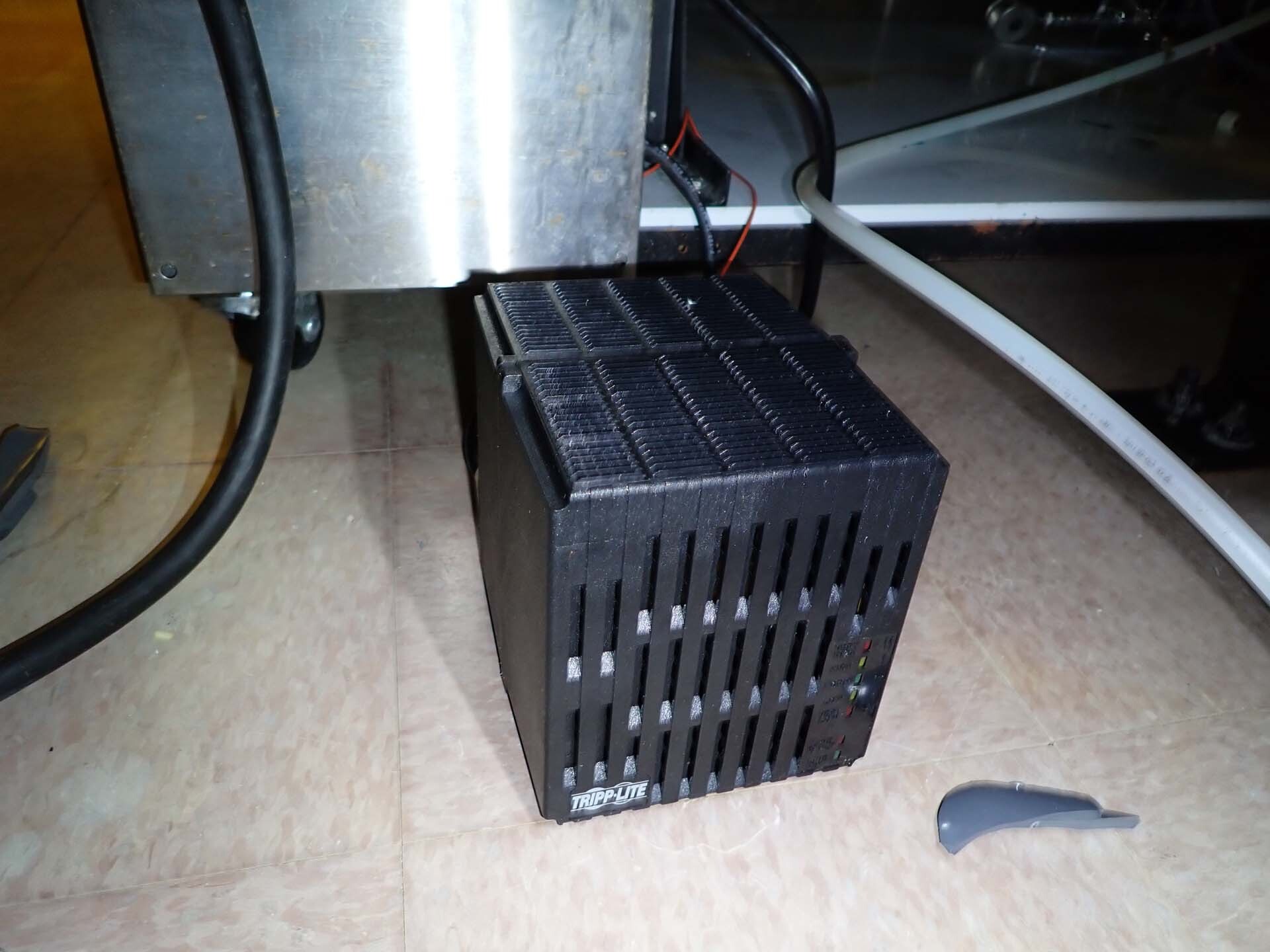
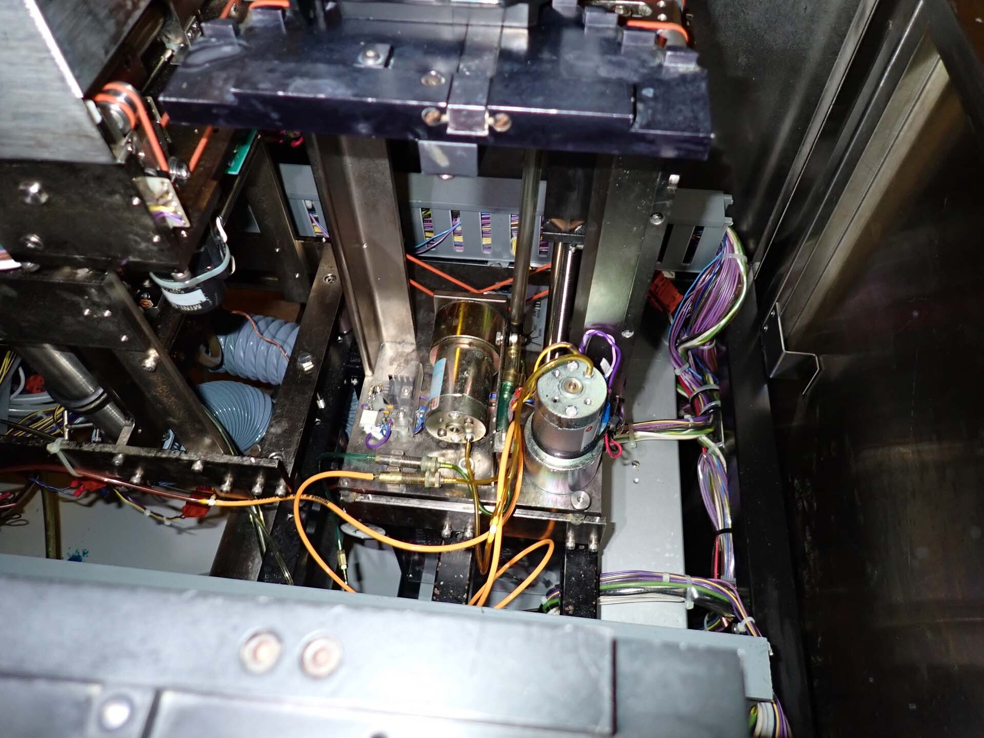
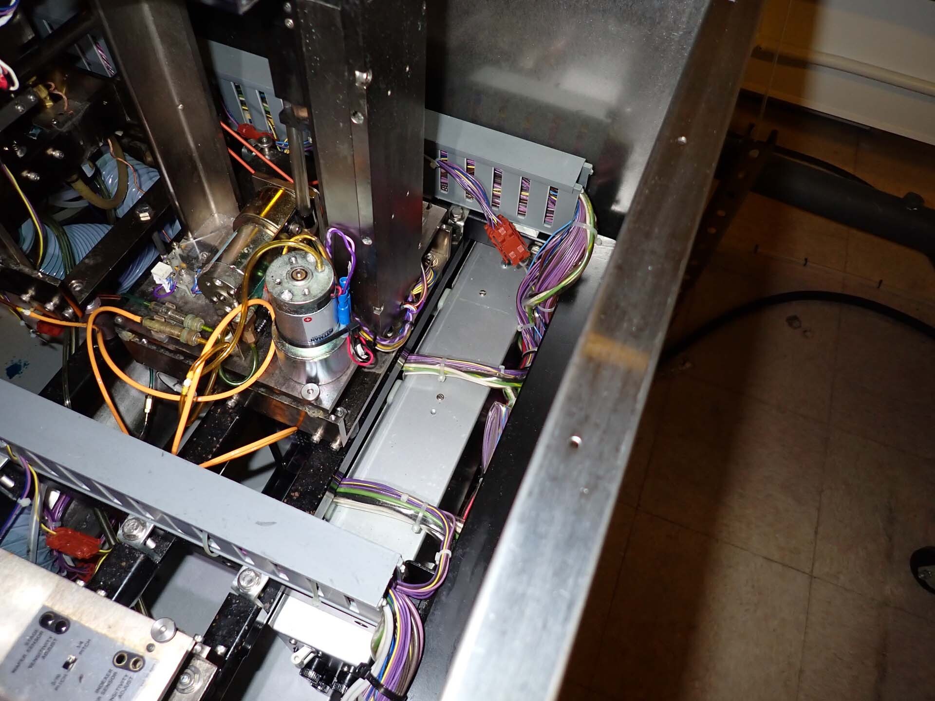
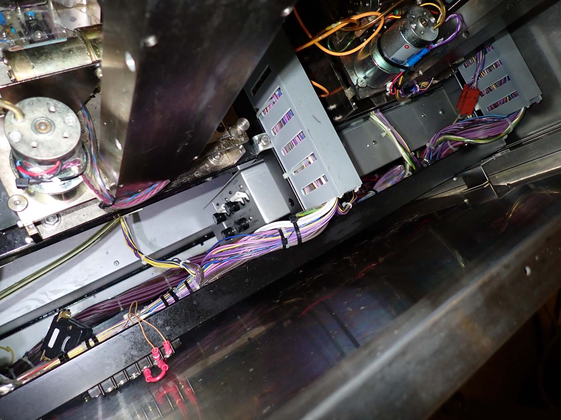
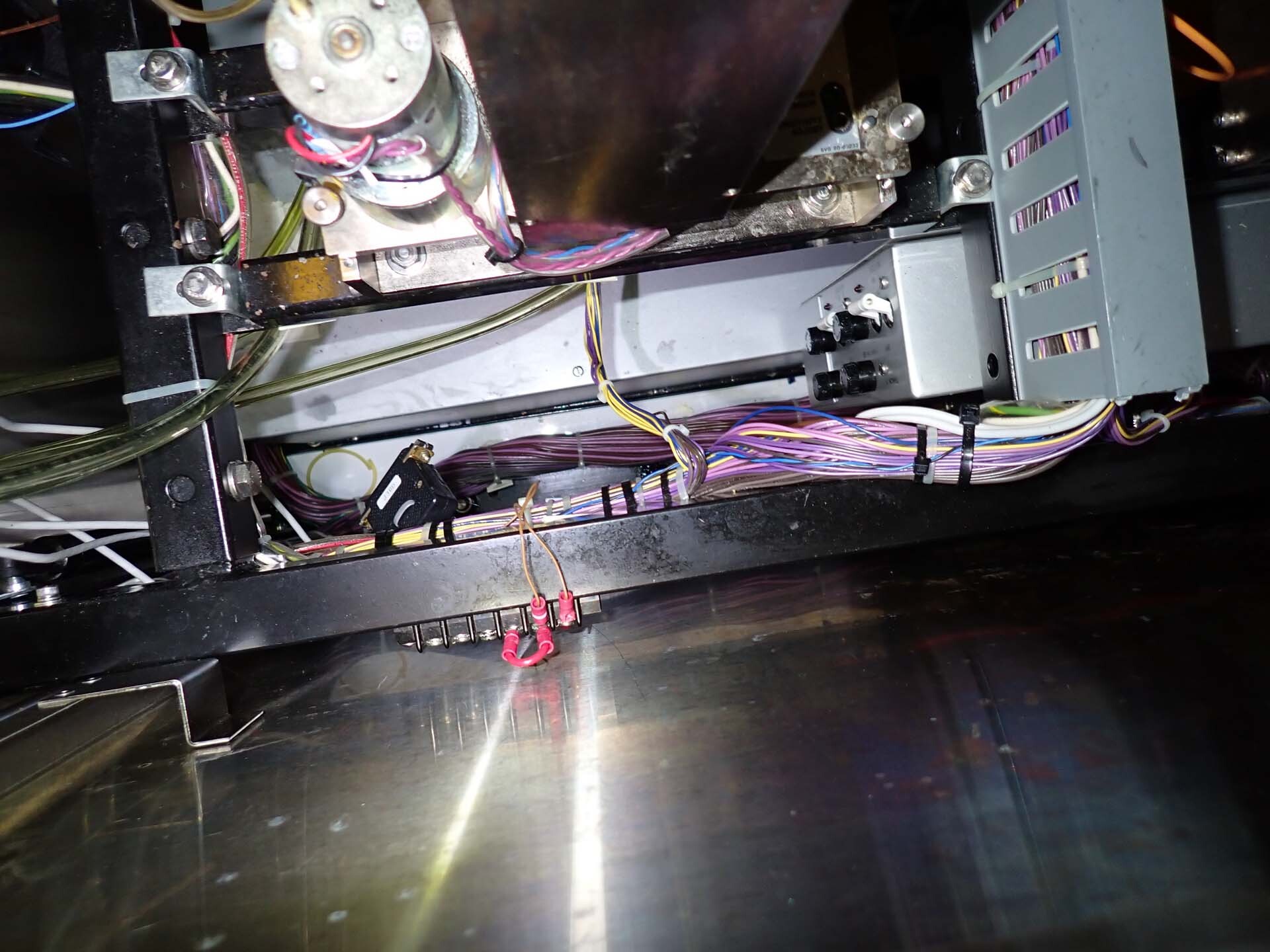
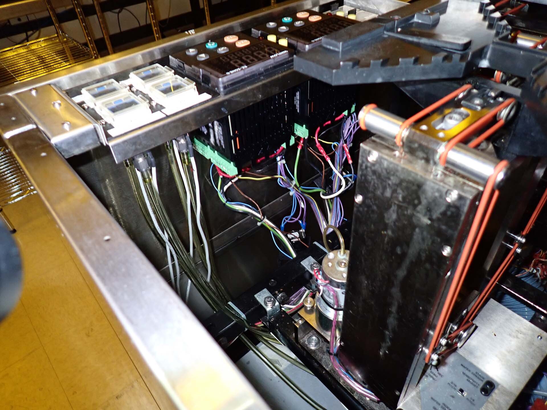
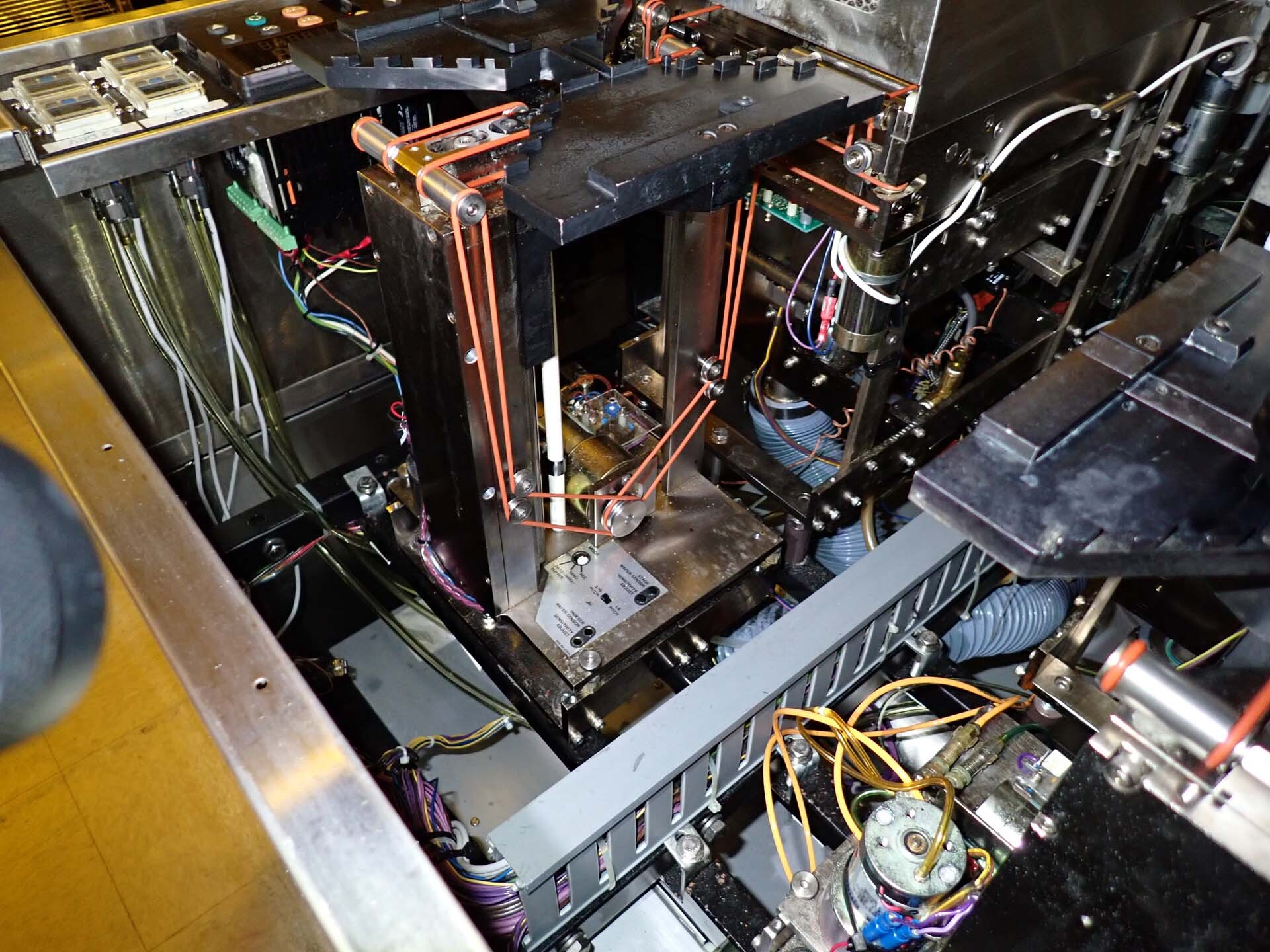
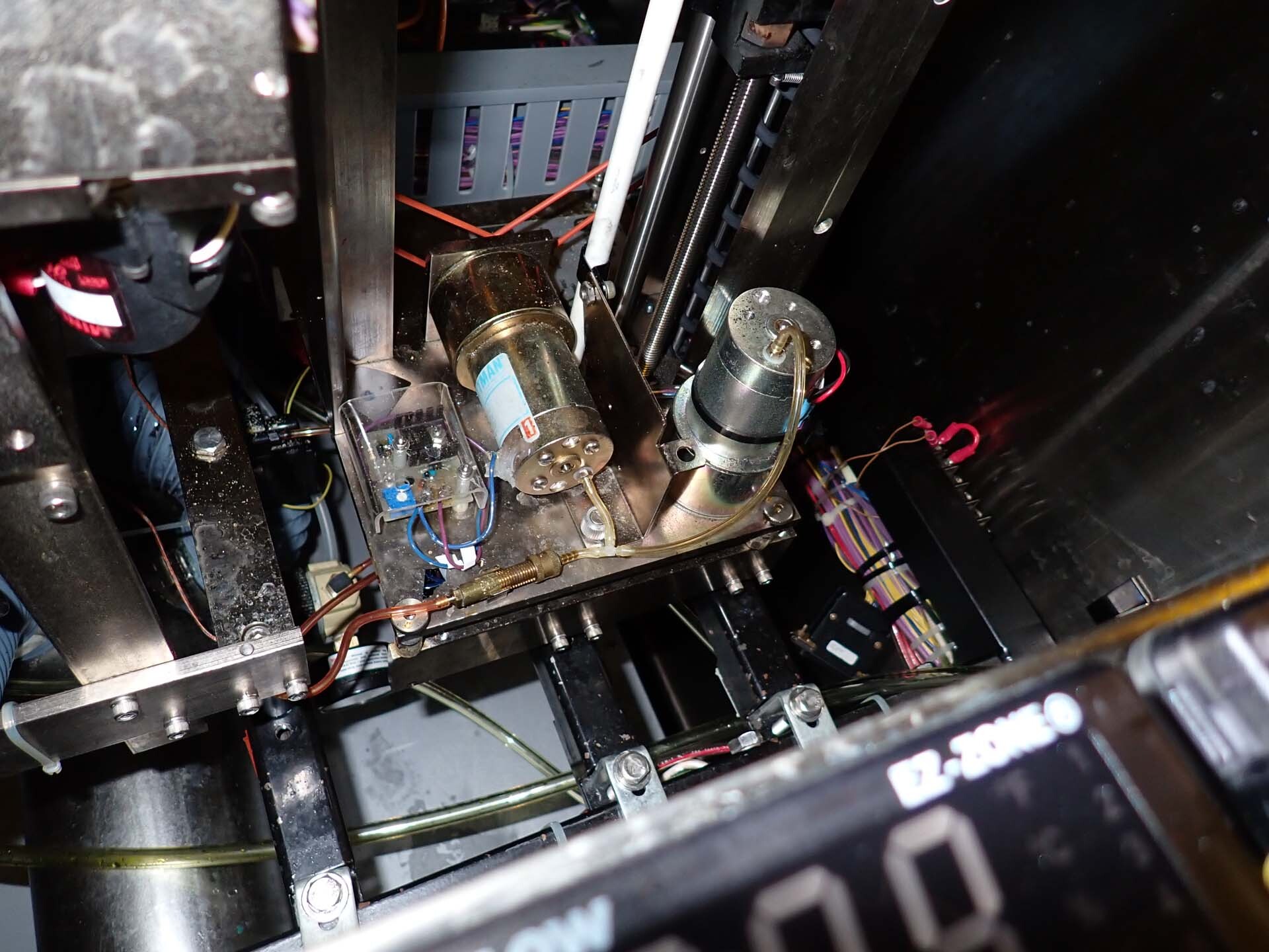
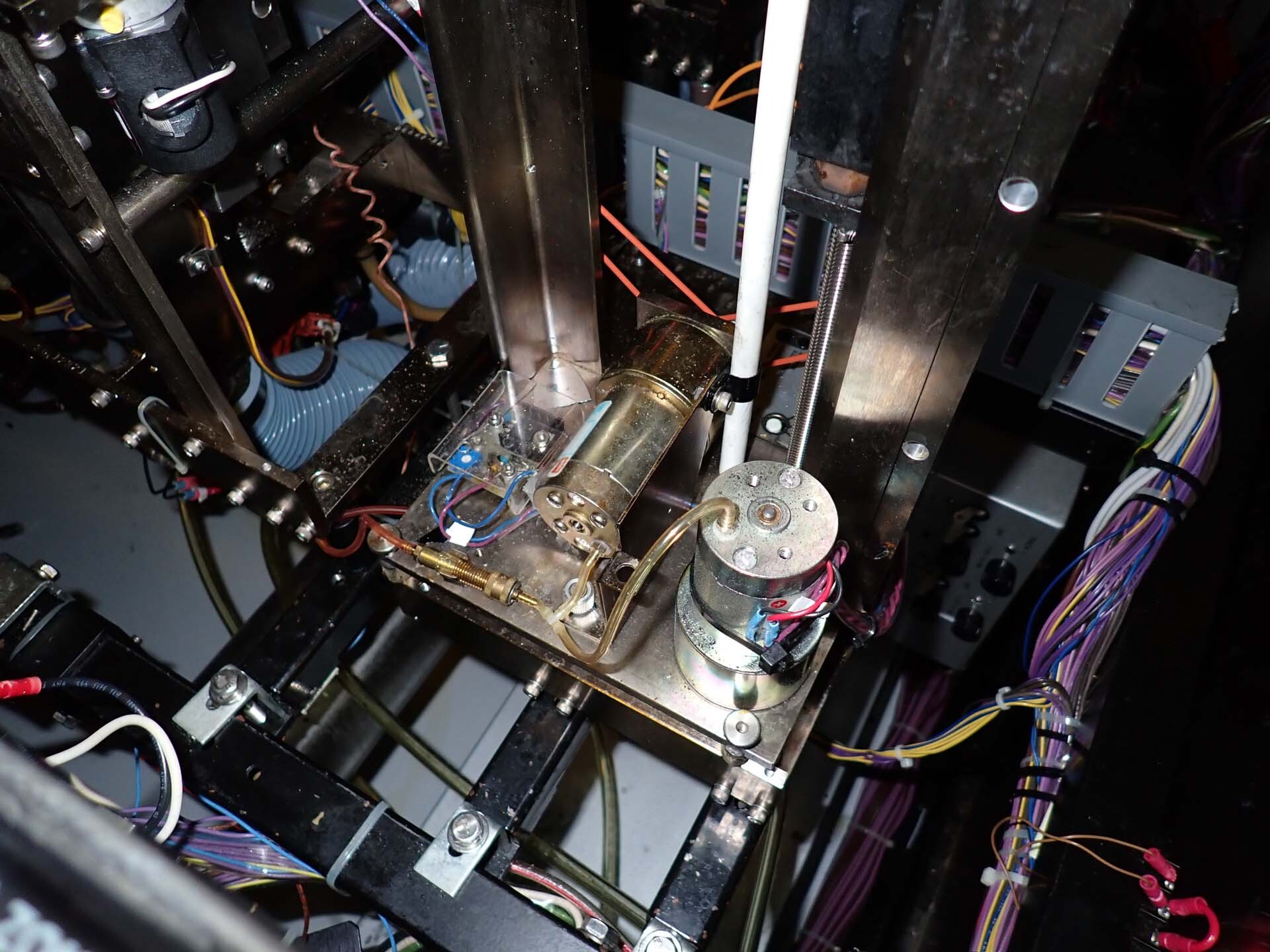
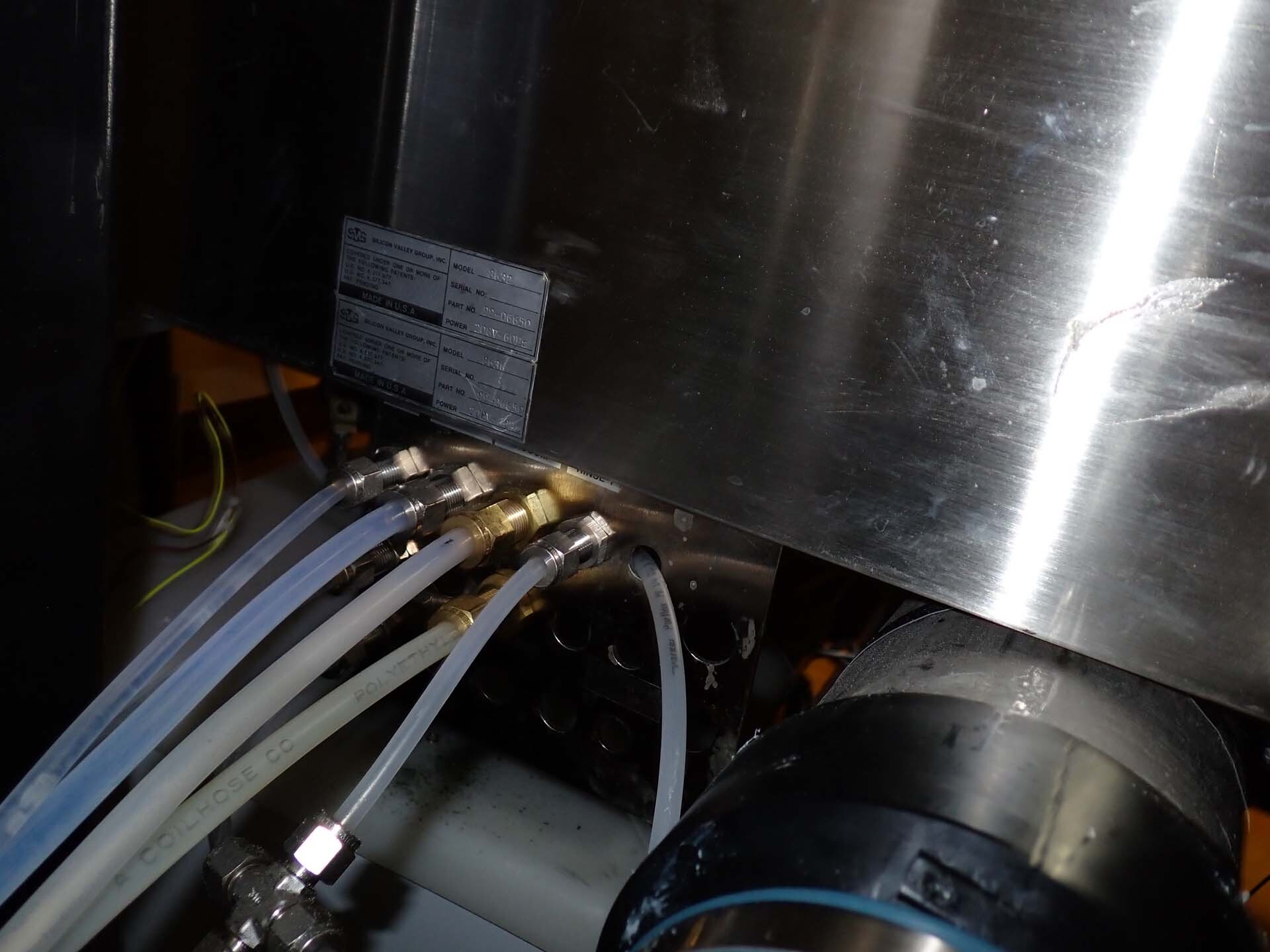
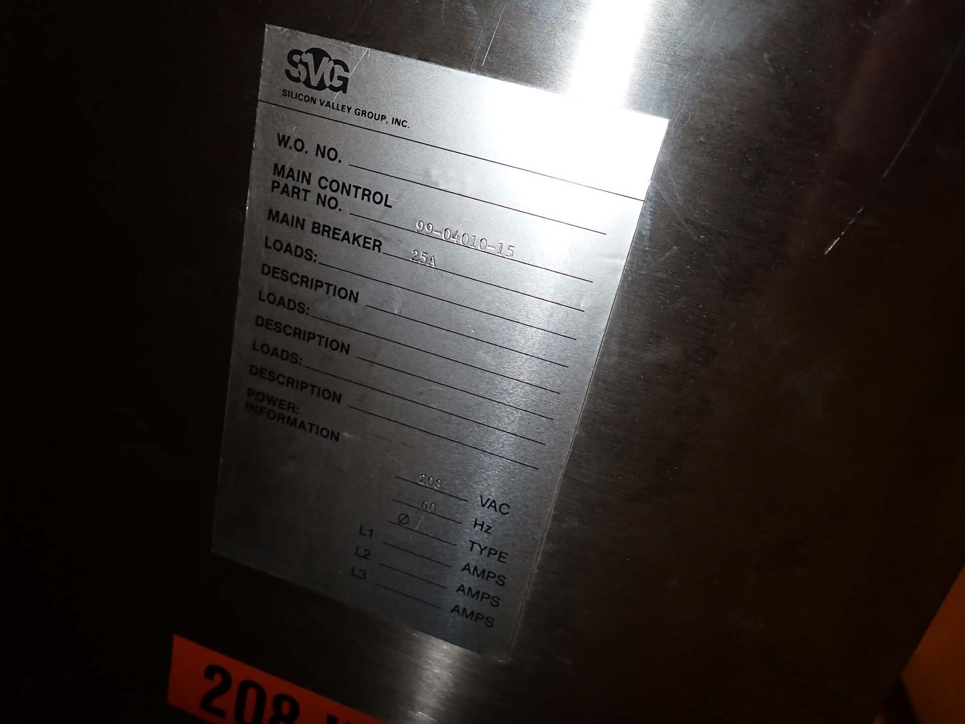
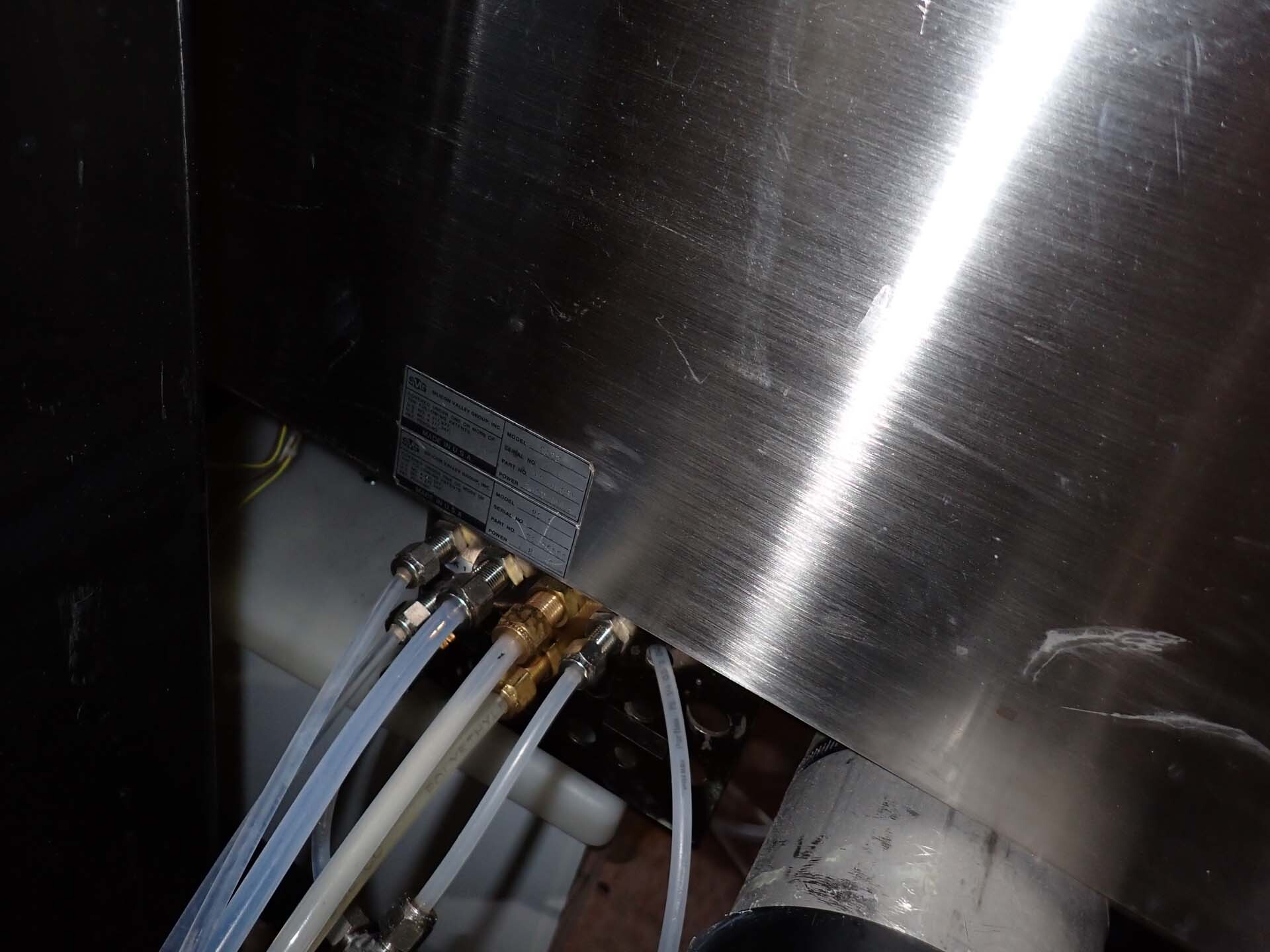
Used SVG (3) Developer systems #293746353 for sale

ID: 293746353
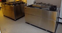
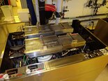
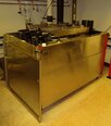
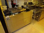
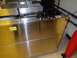
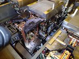
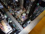
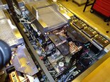
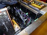
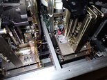
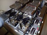
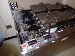
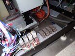
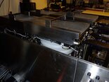
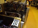
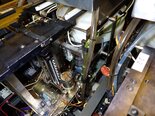
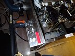
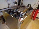
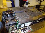
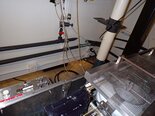
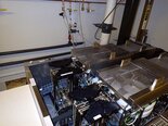
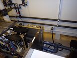
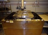
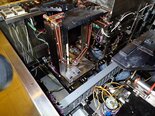
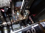
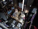
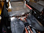
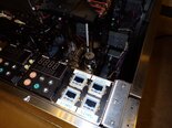
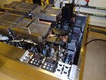
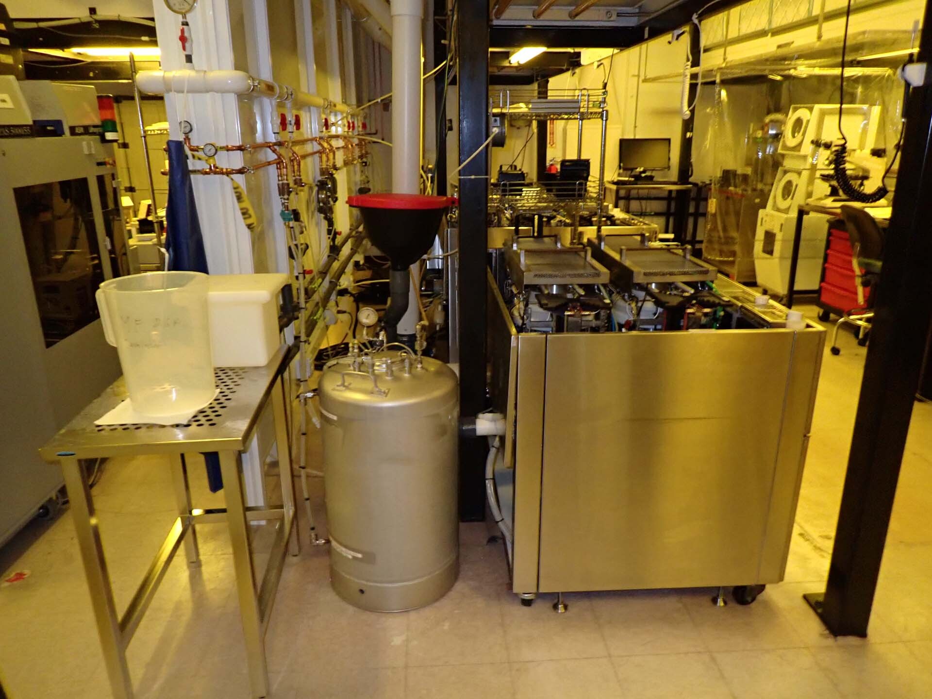
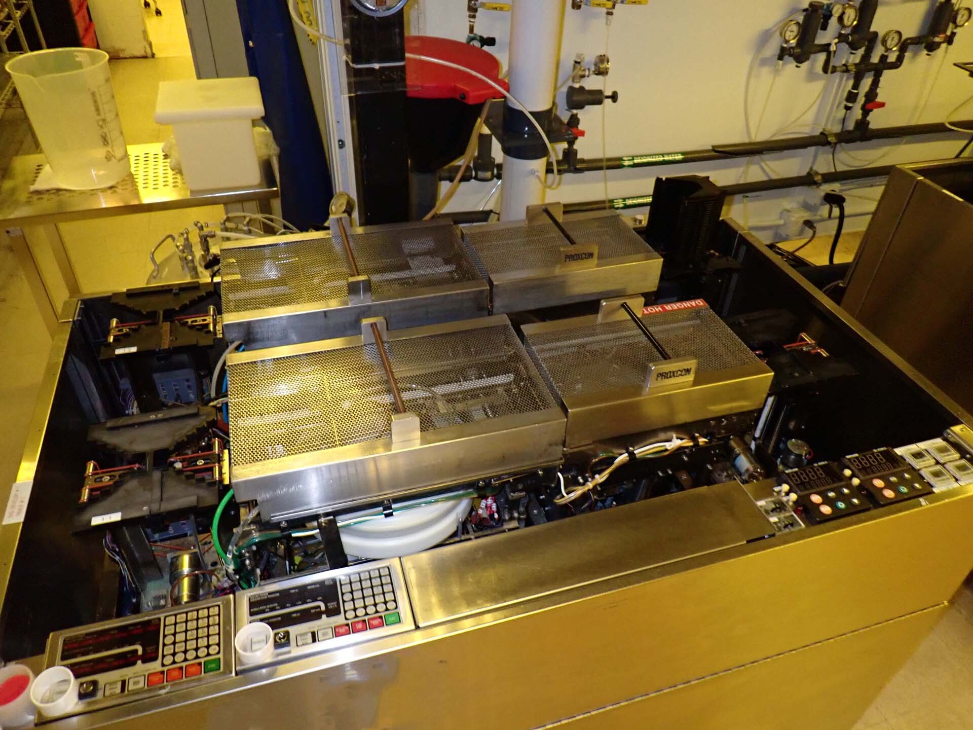
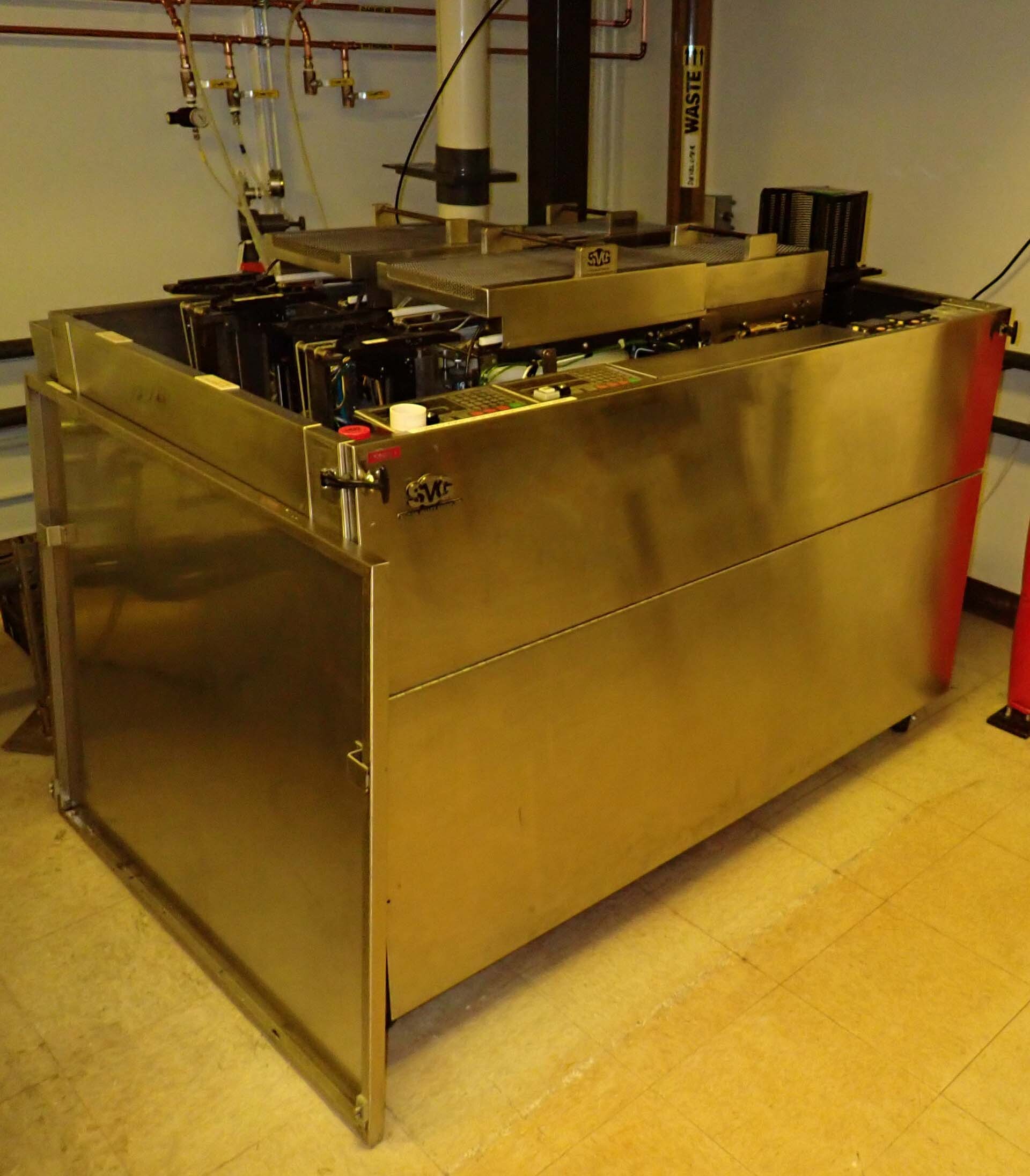
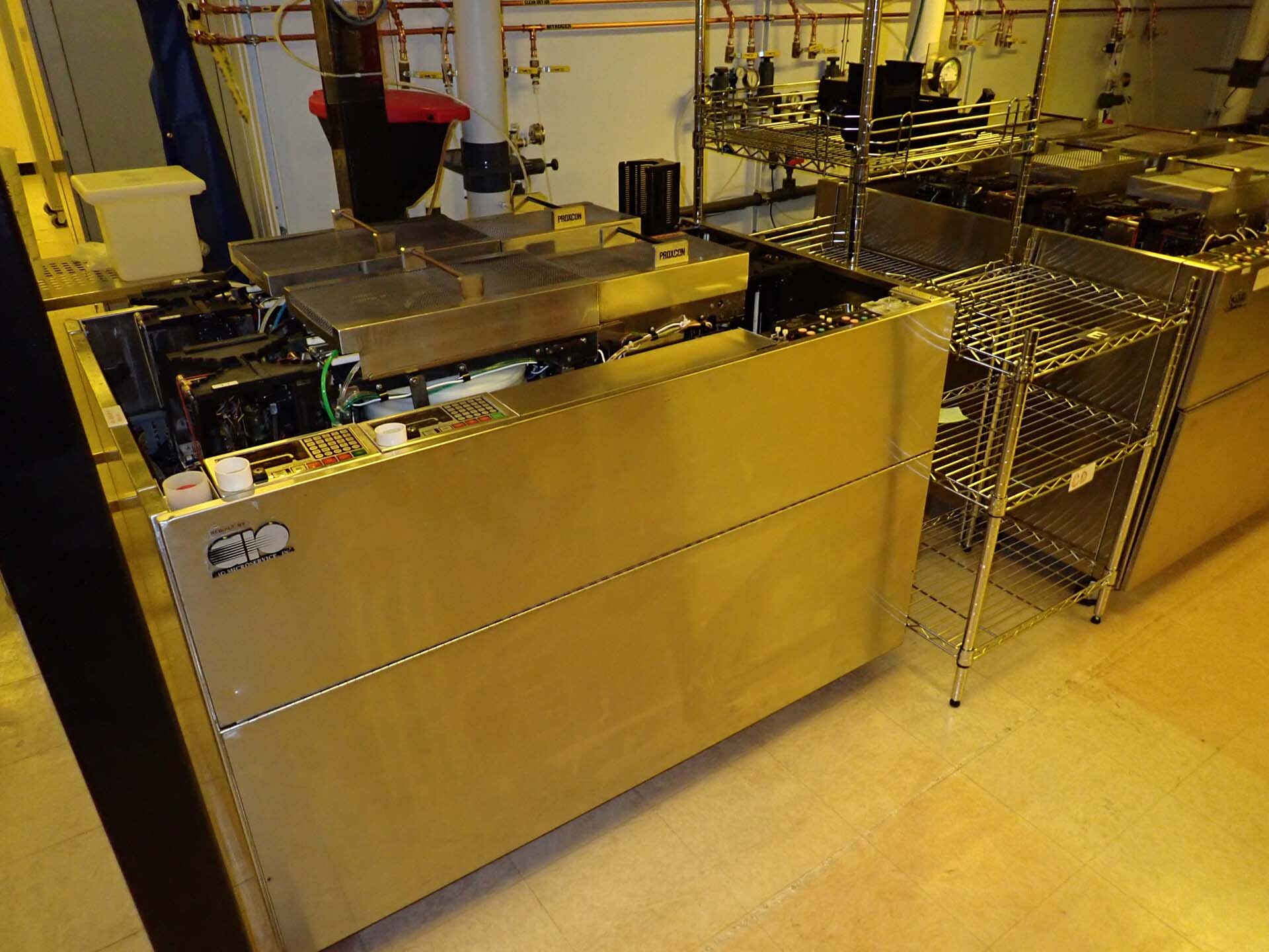
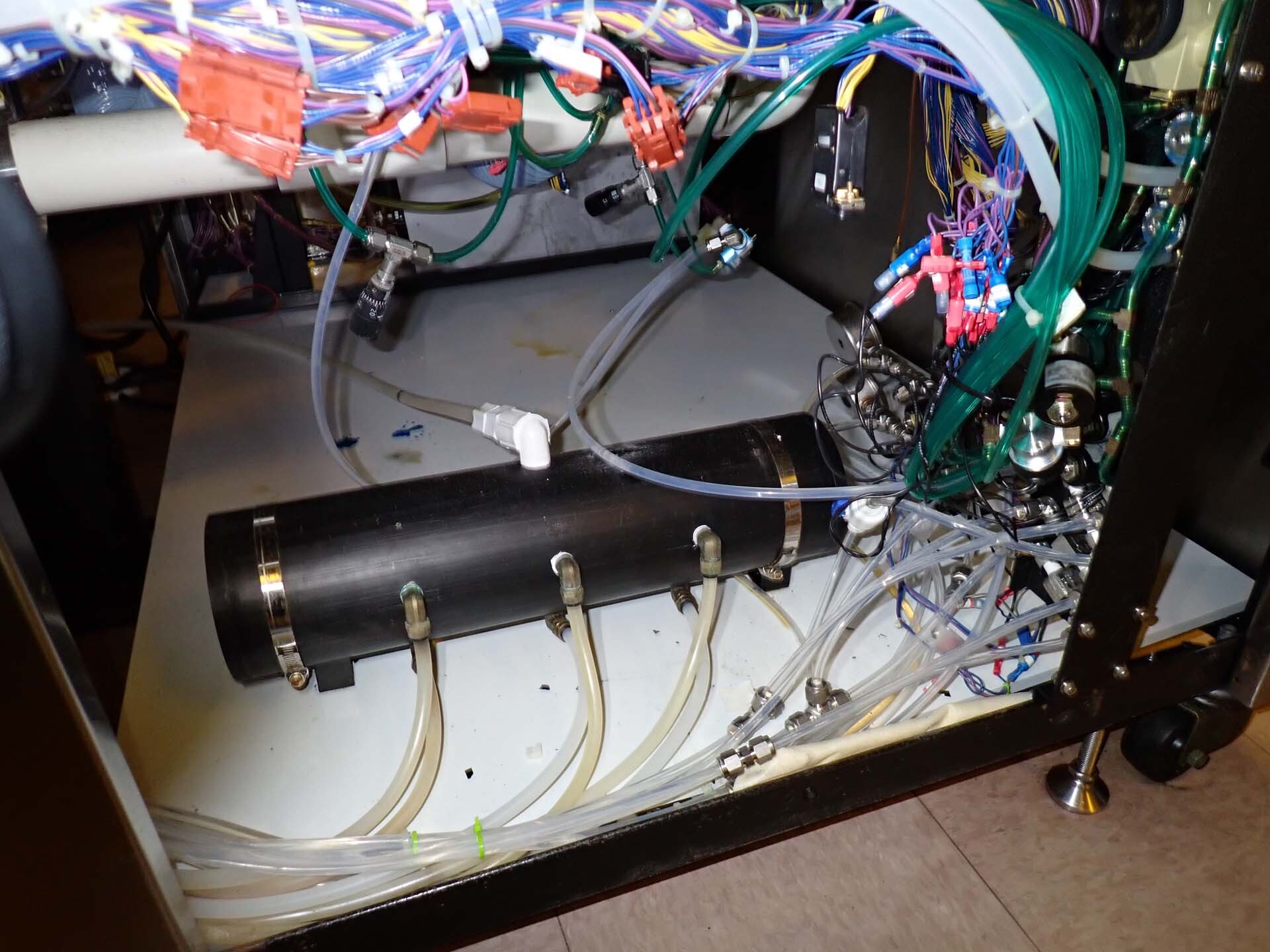
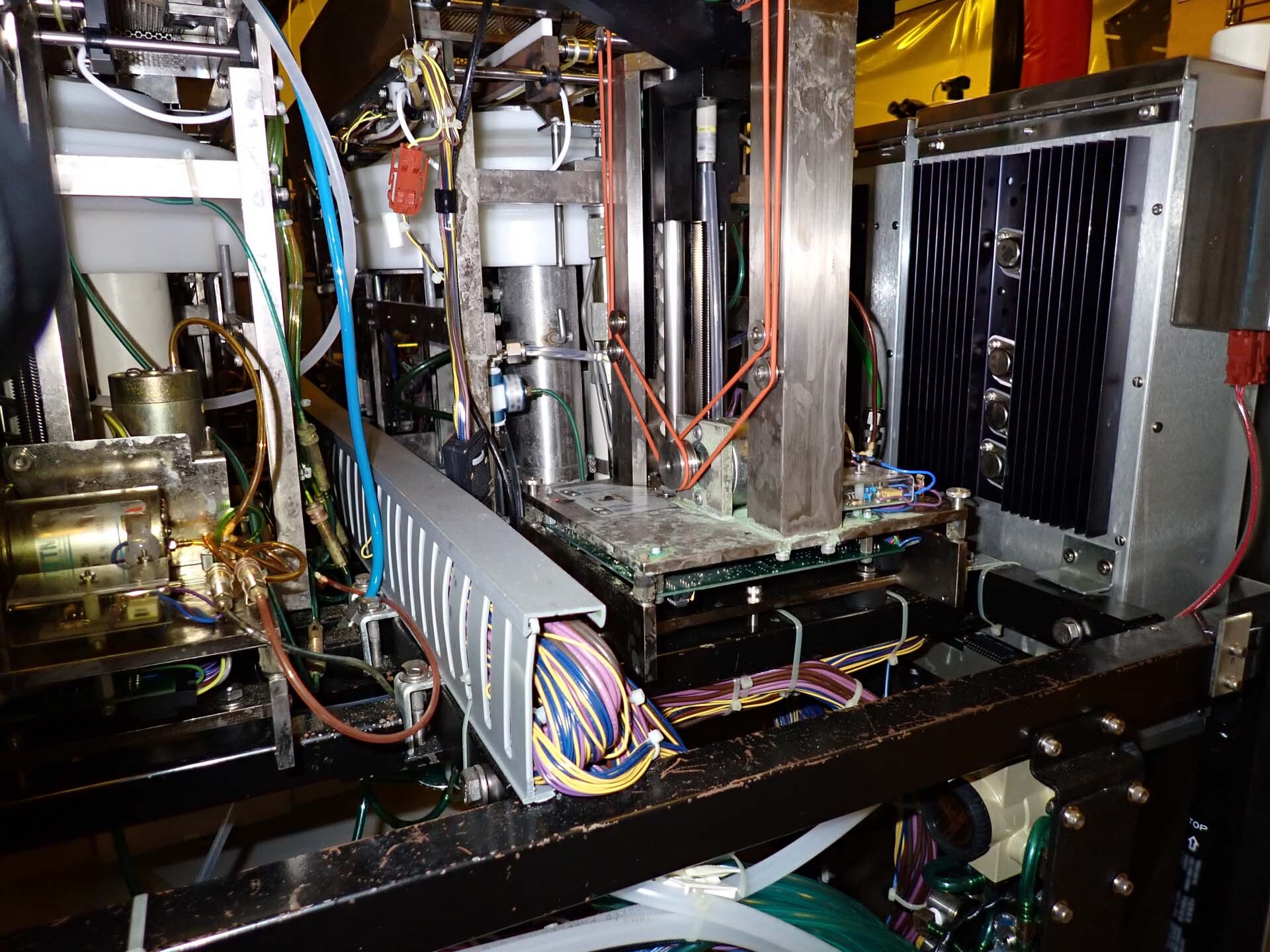
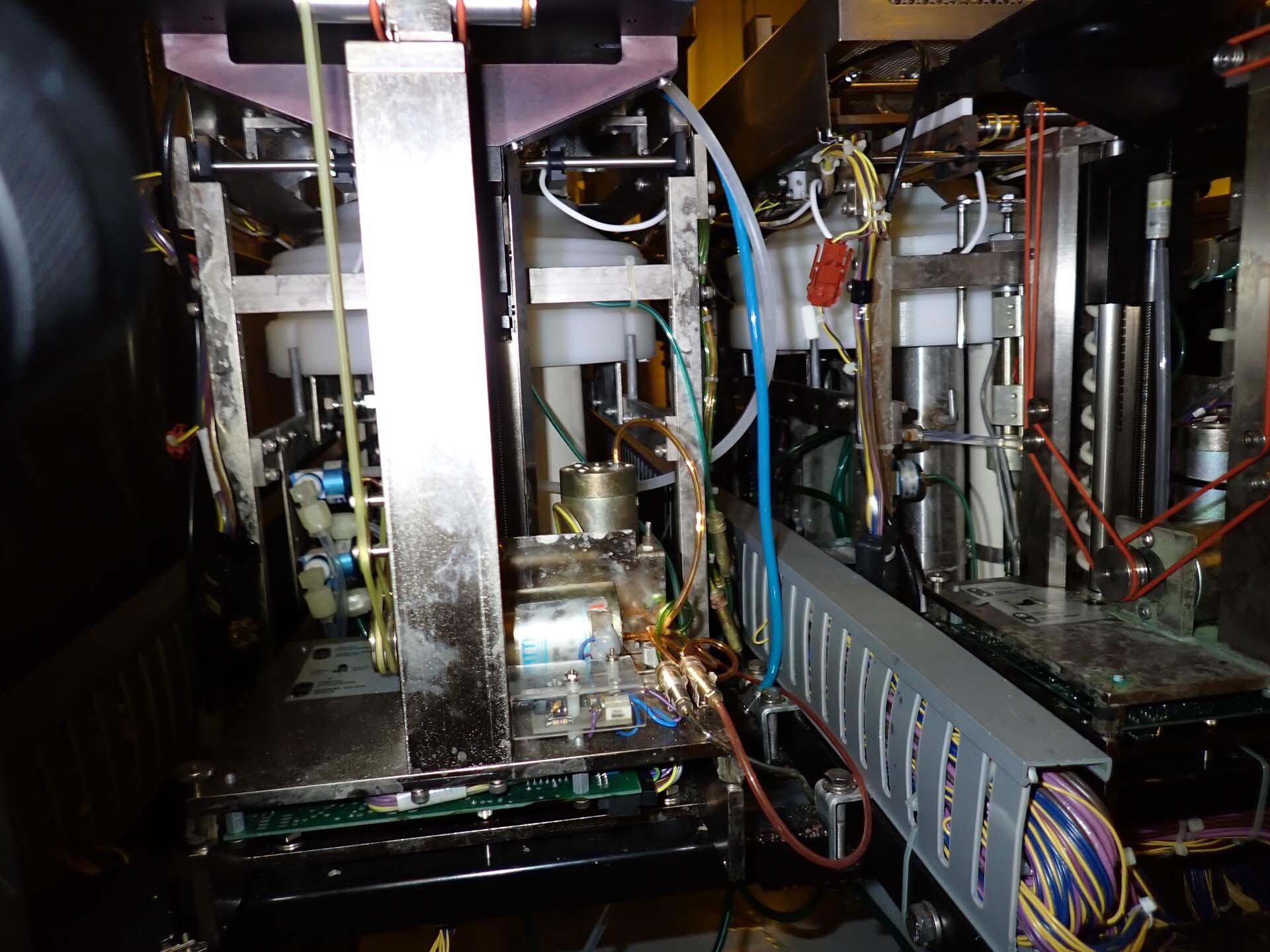
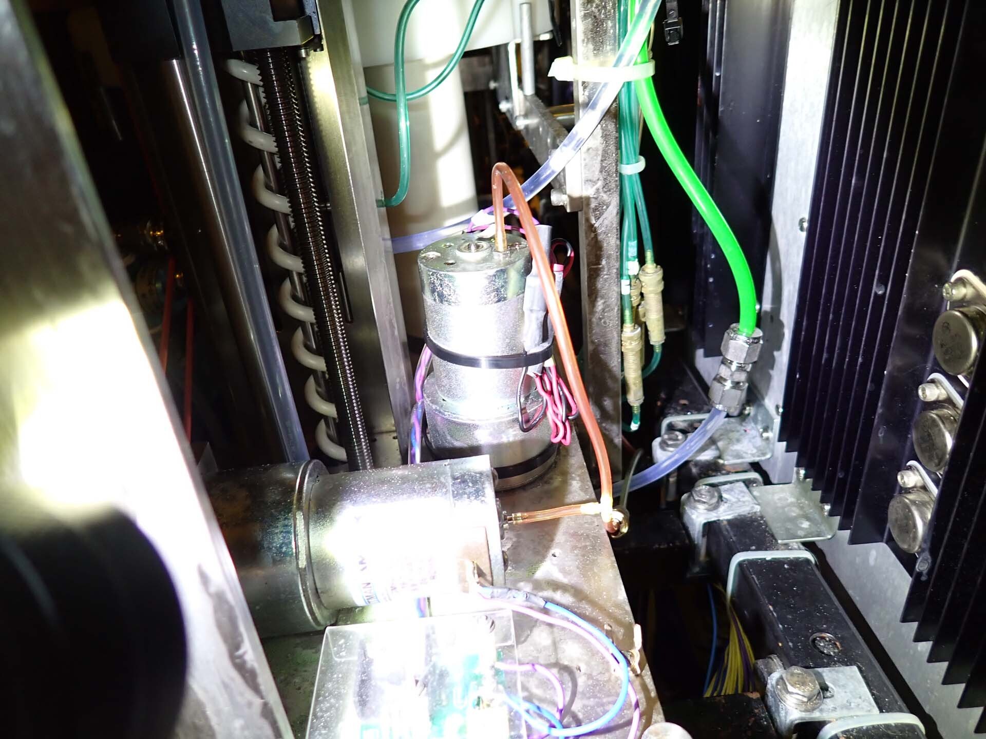
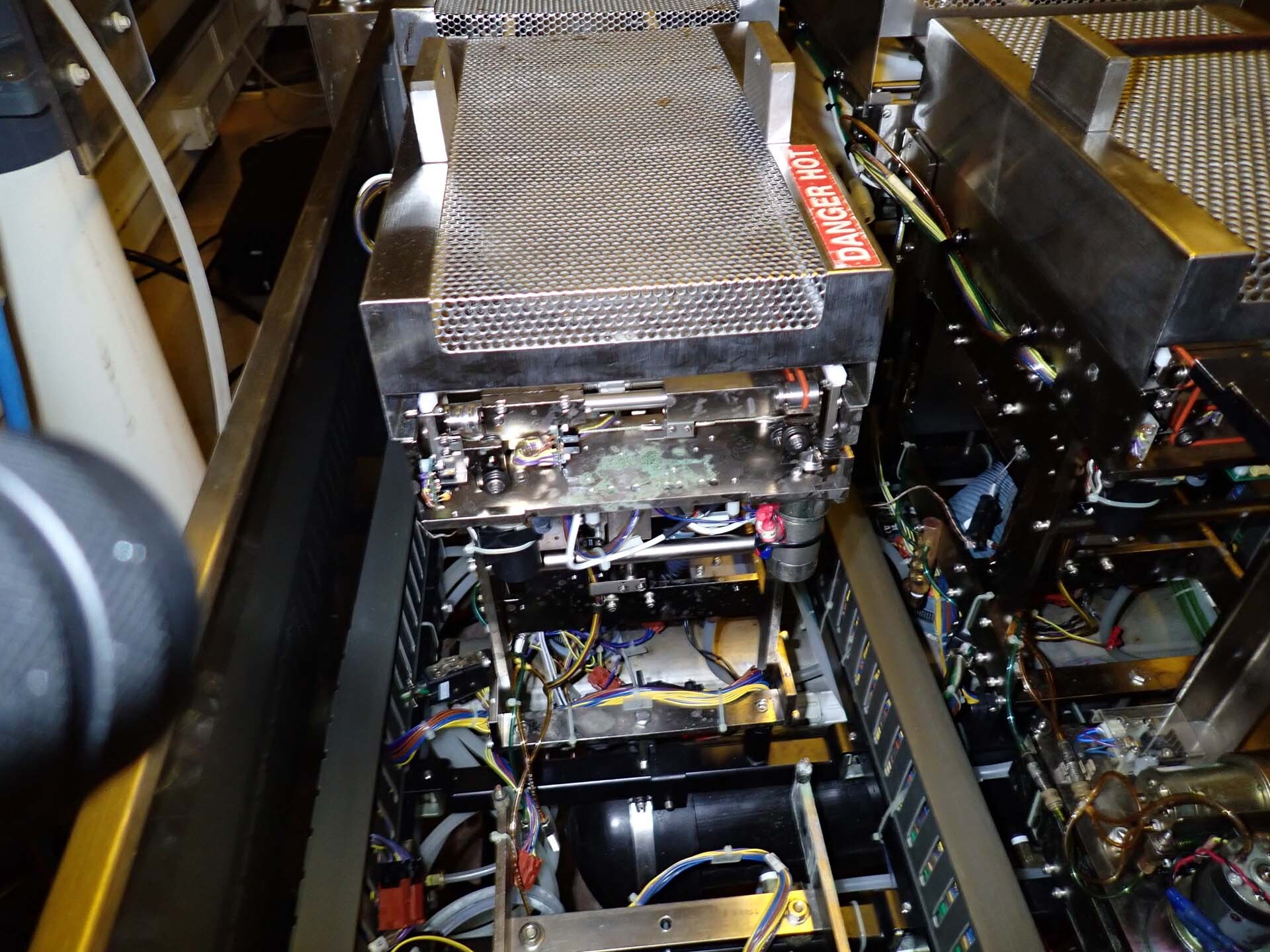
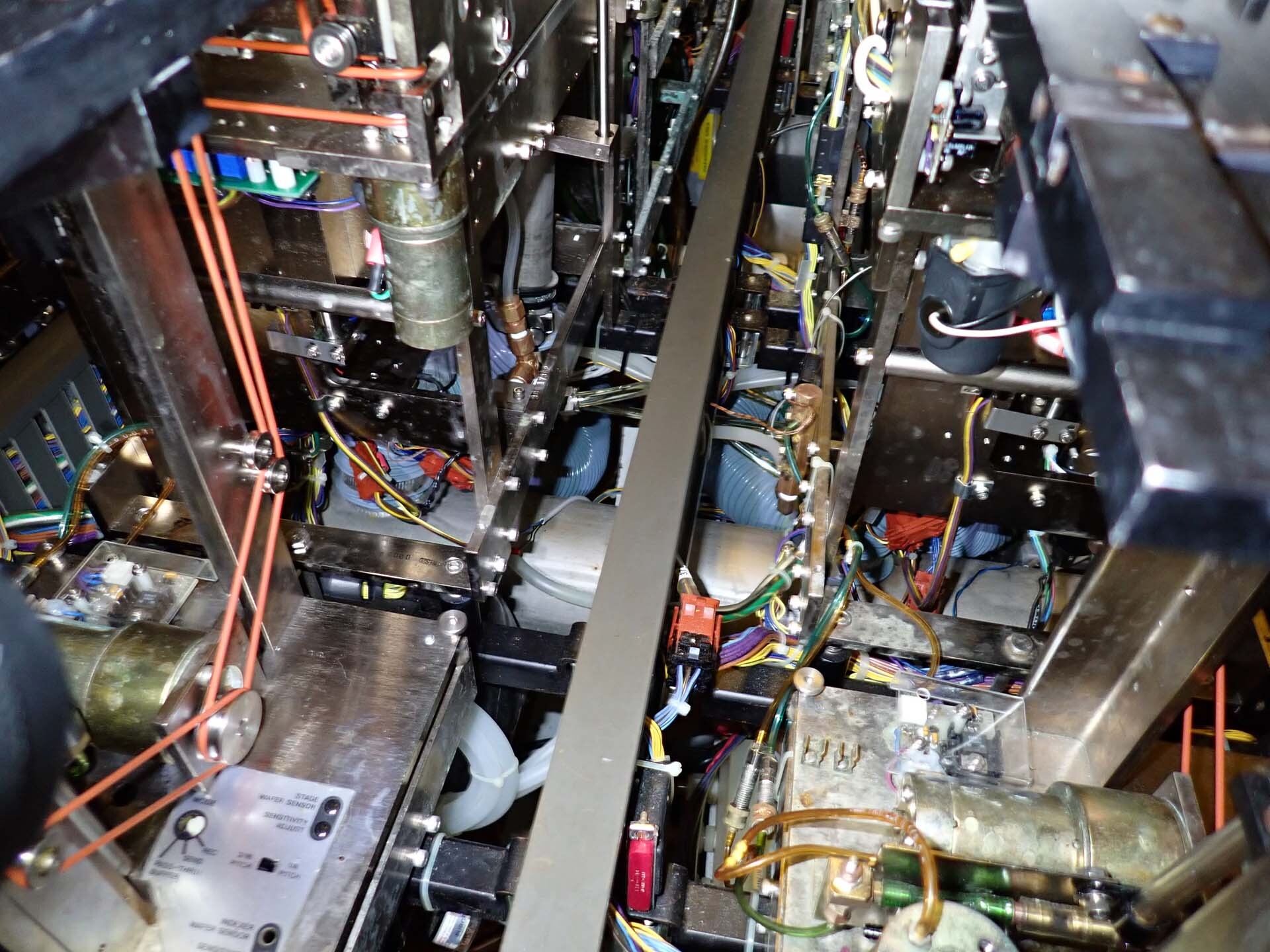
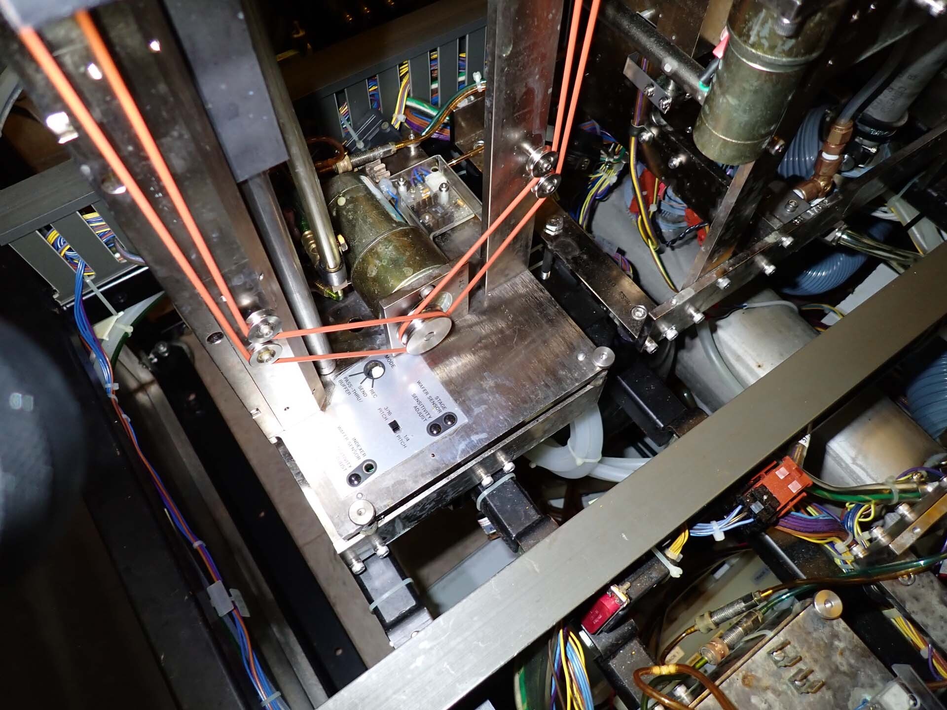
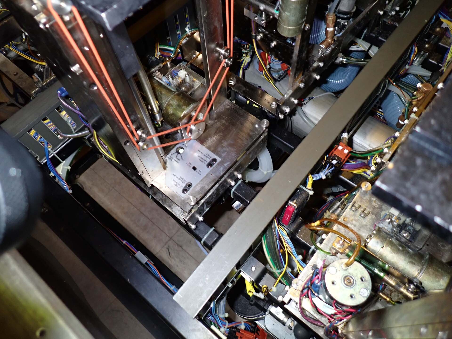
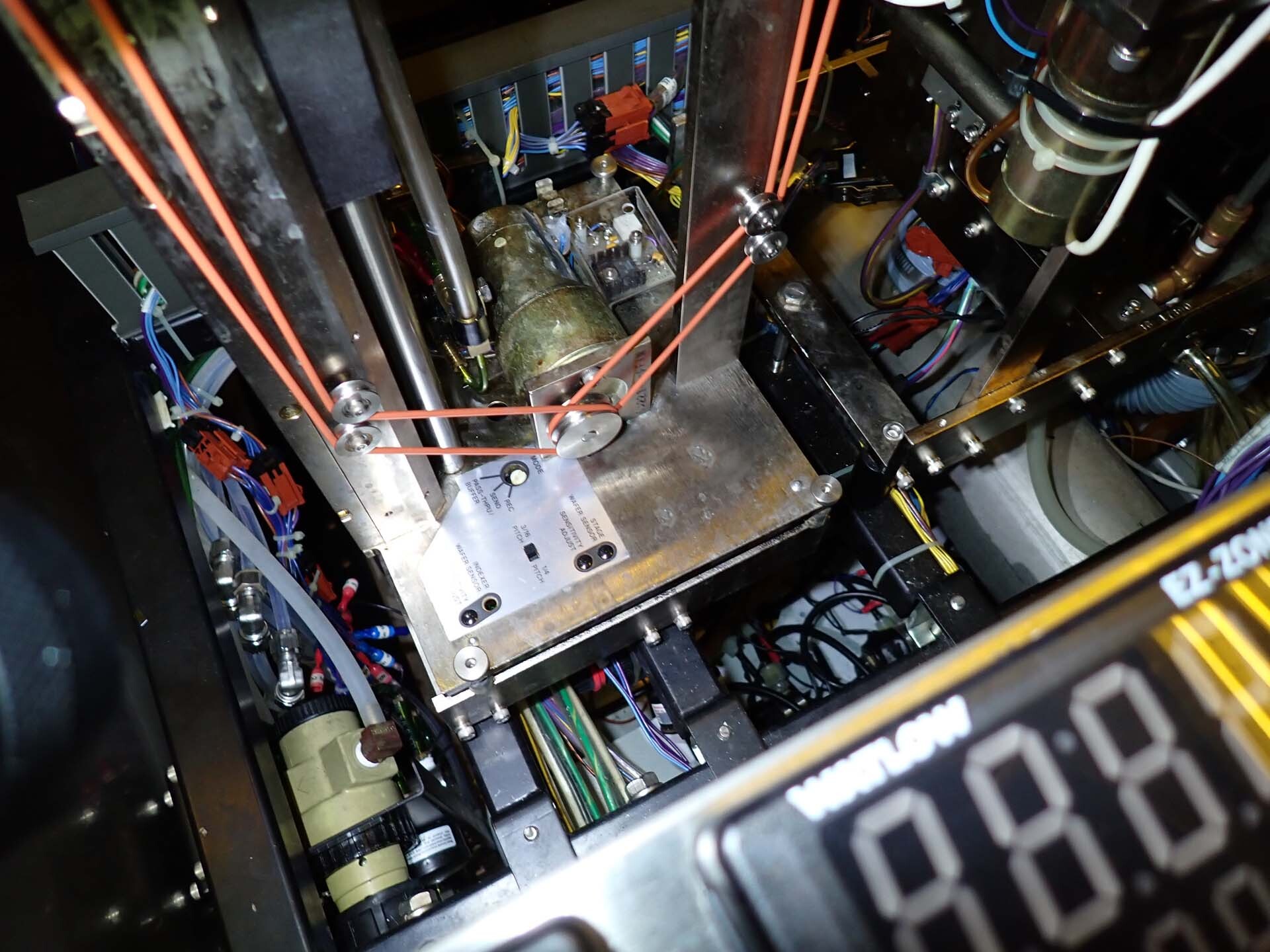
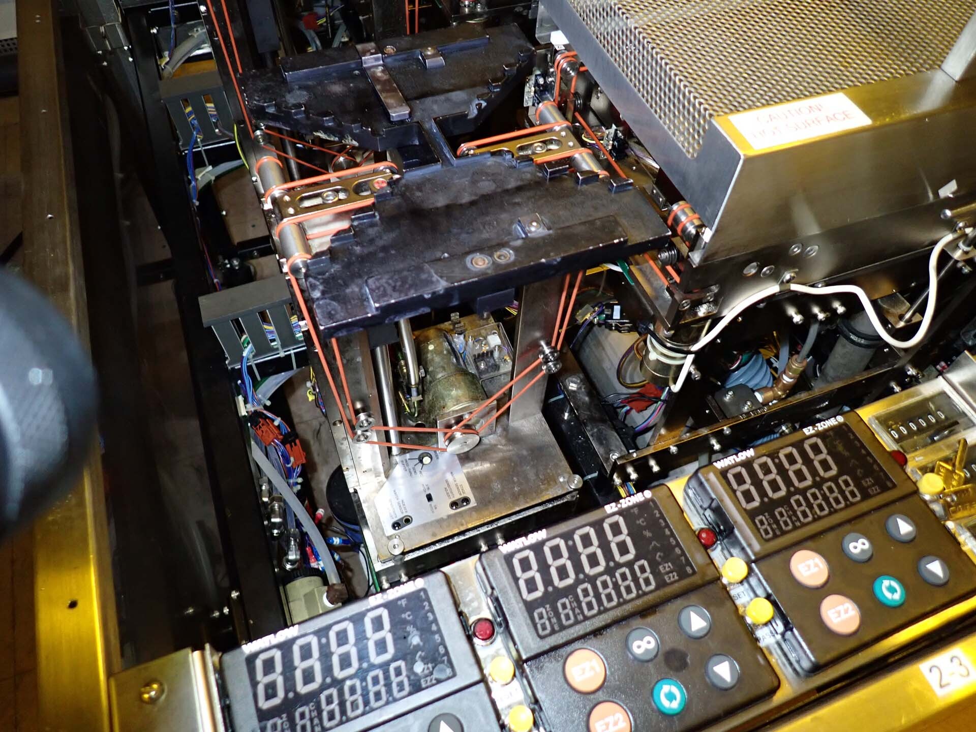
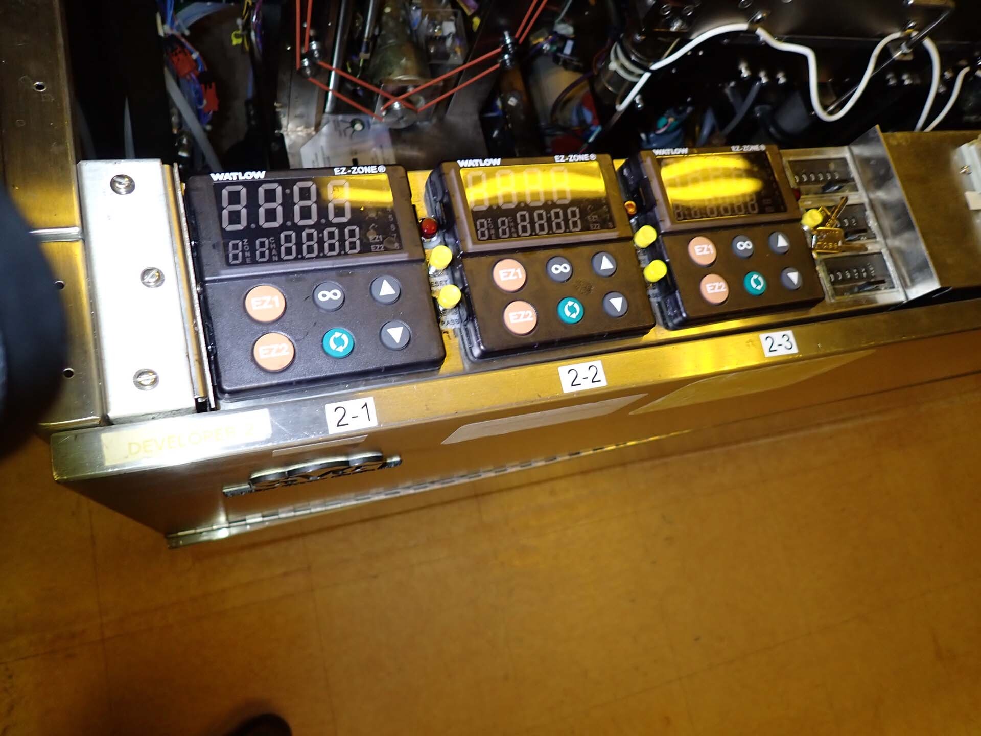
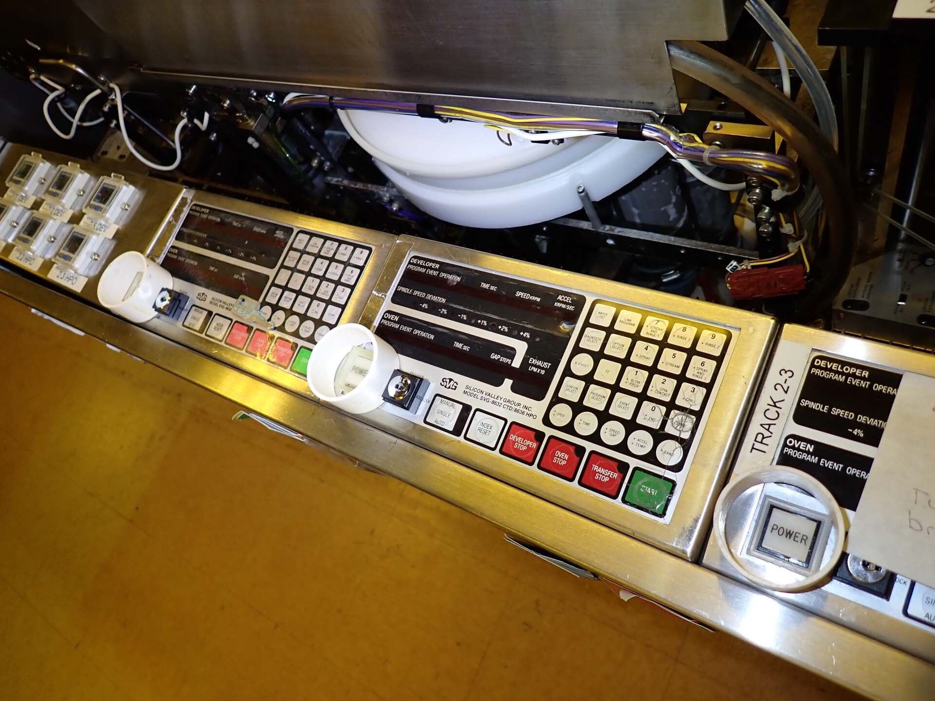
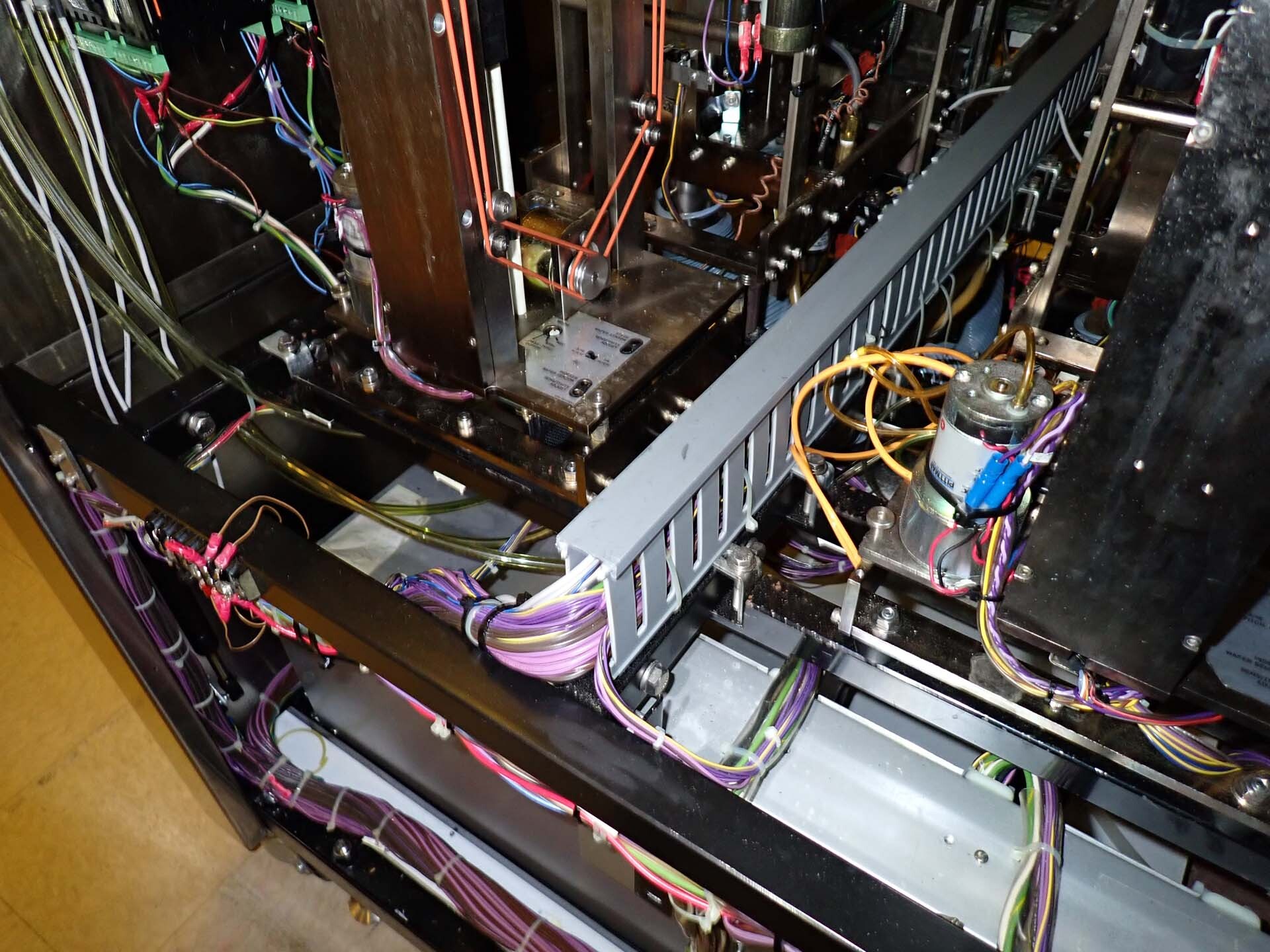
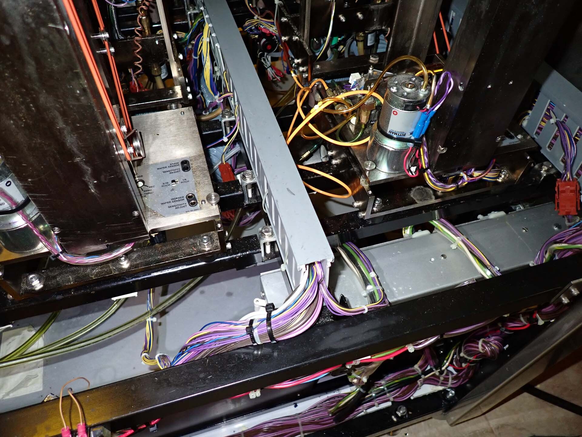
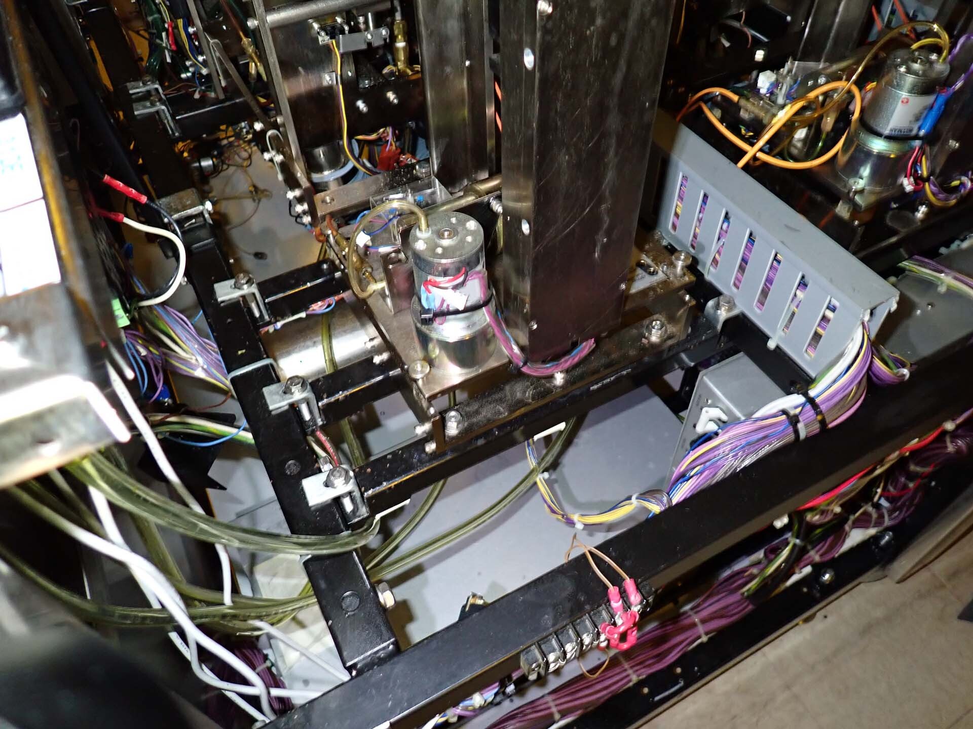
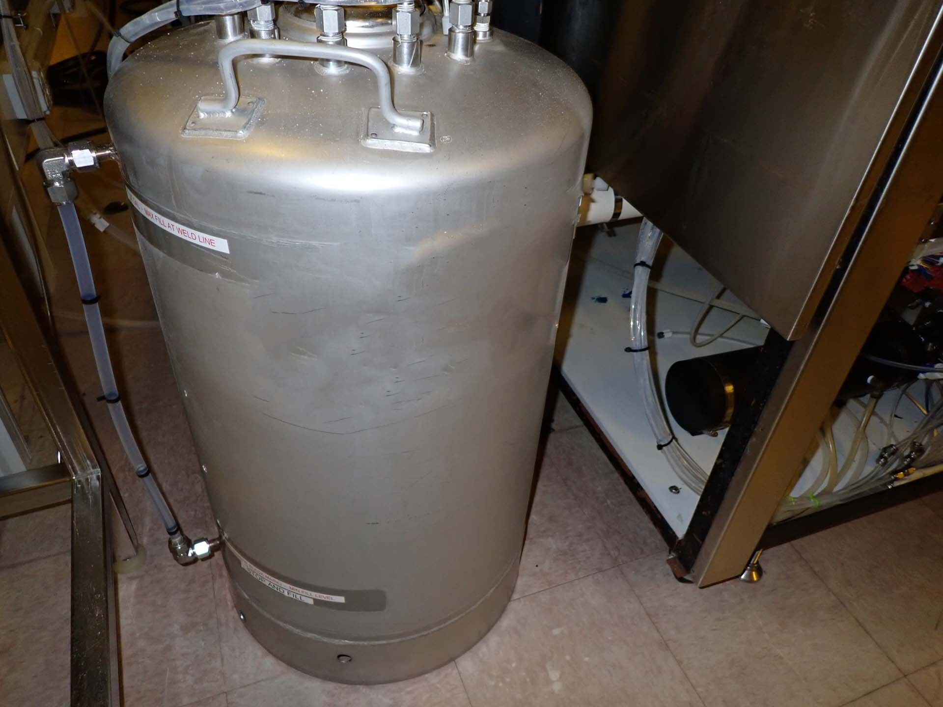
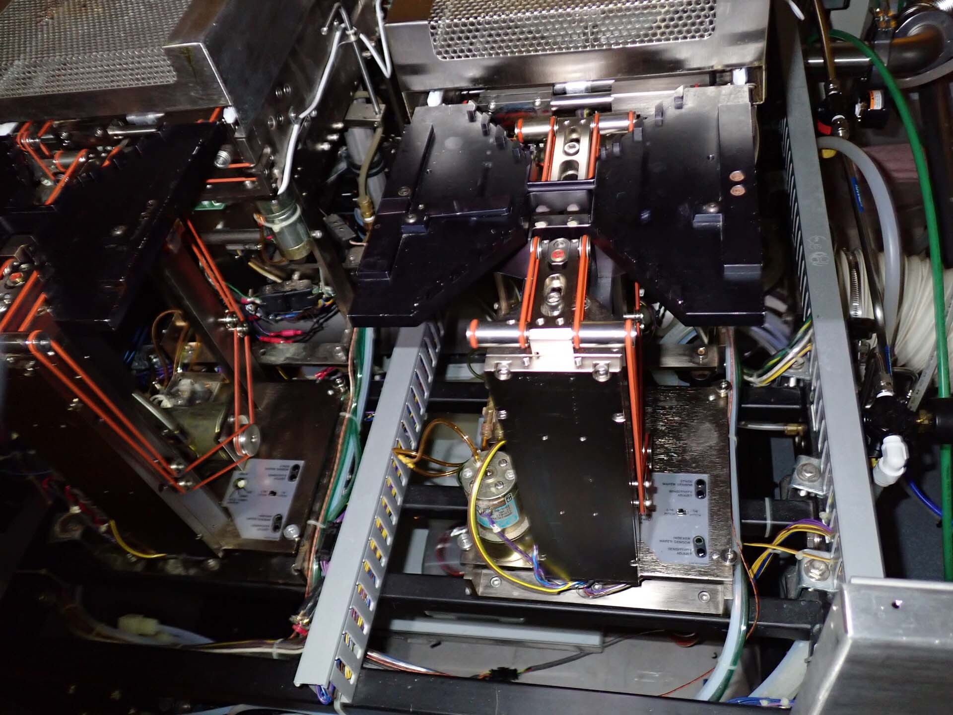
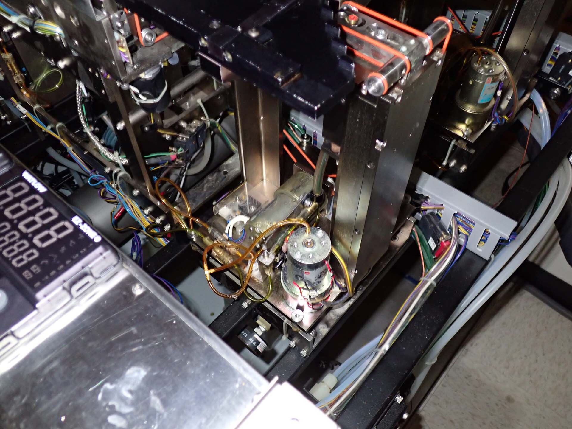
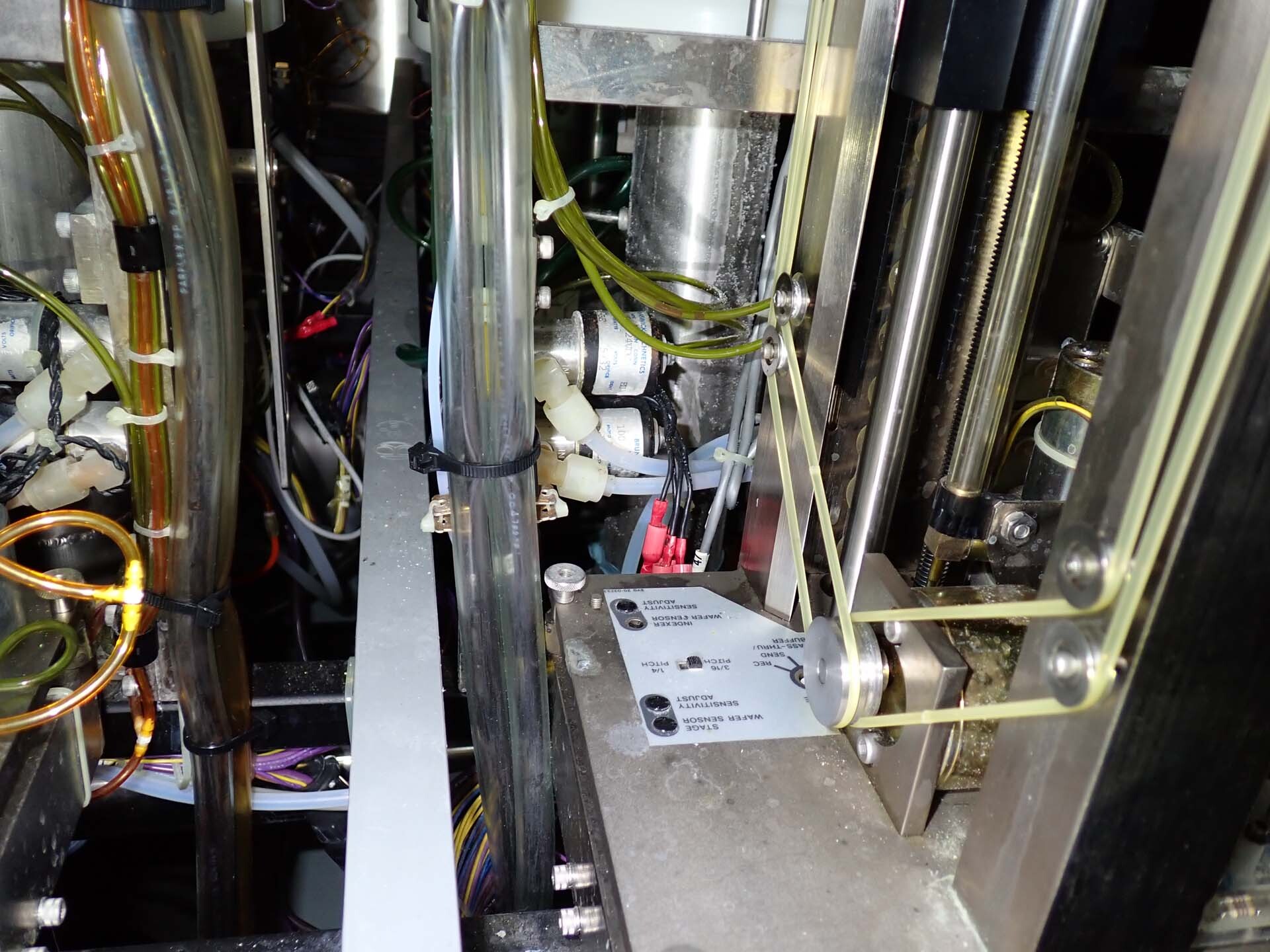
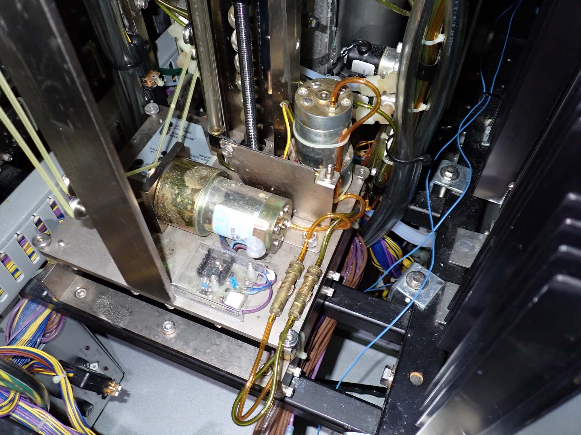
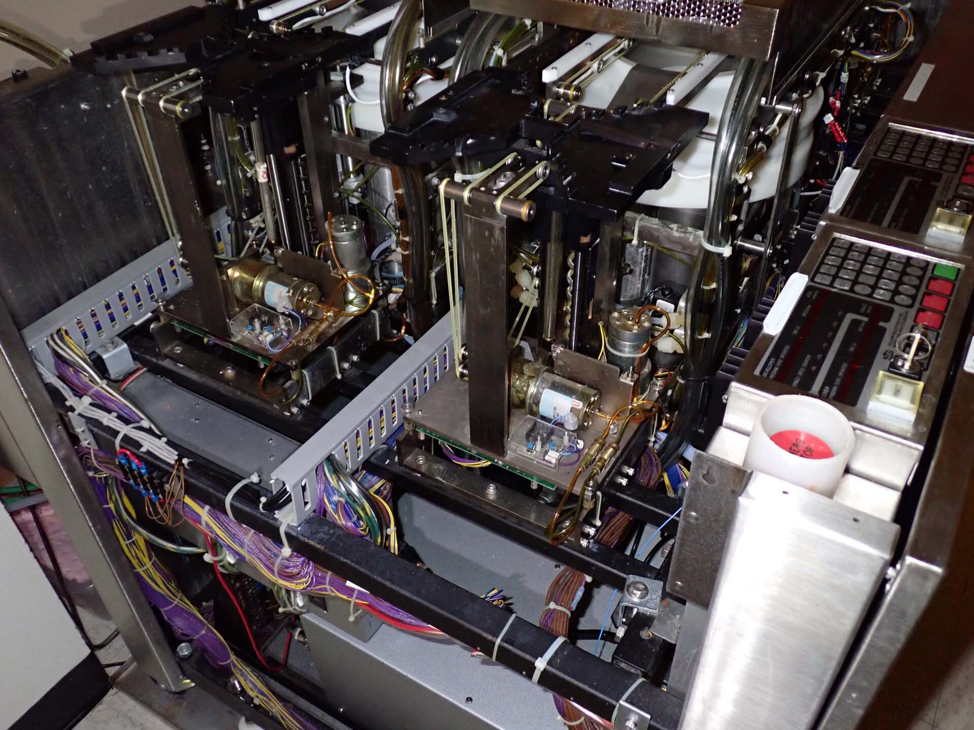
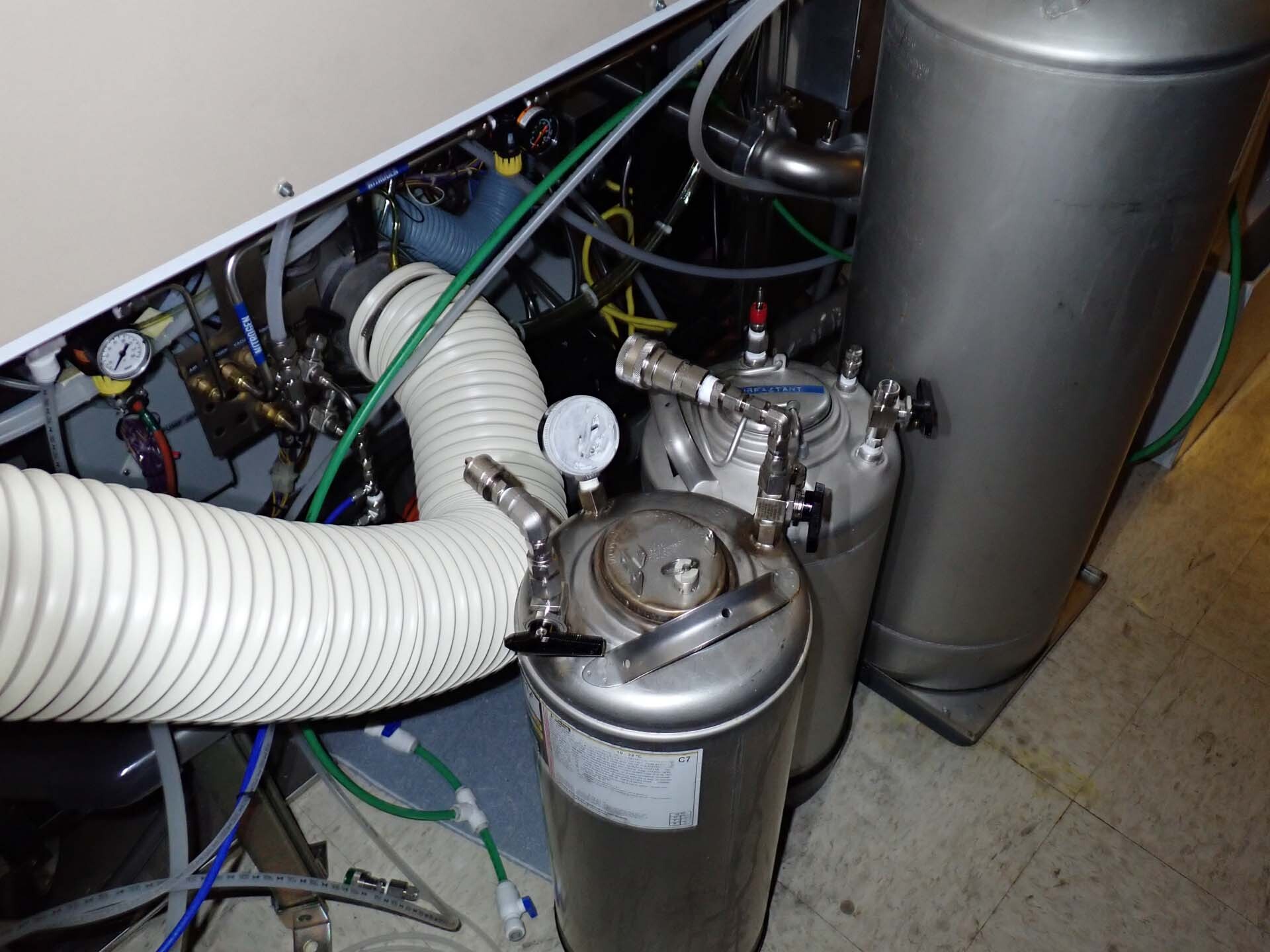
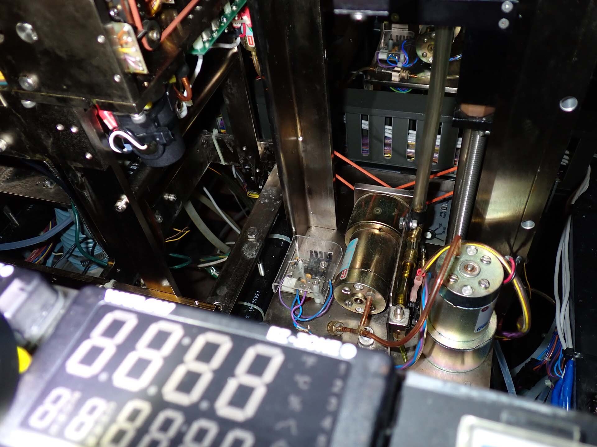
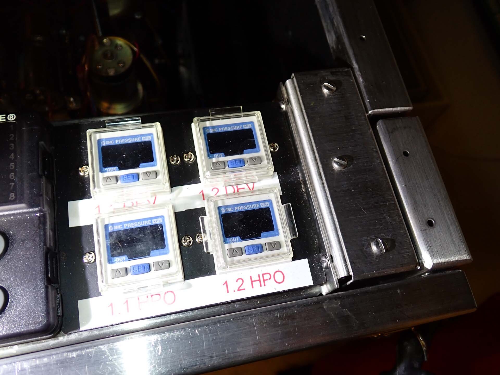
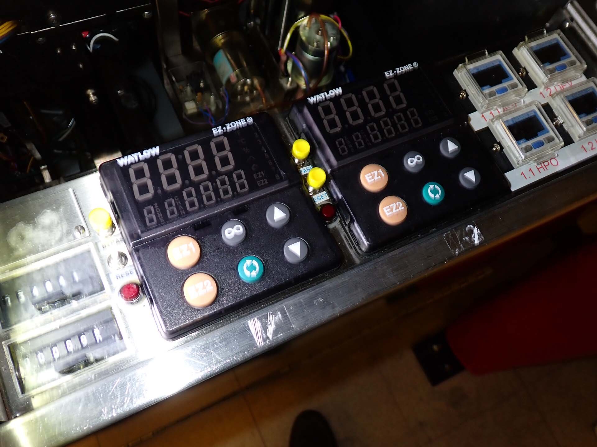
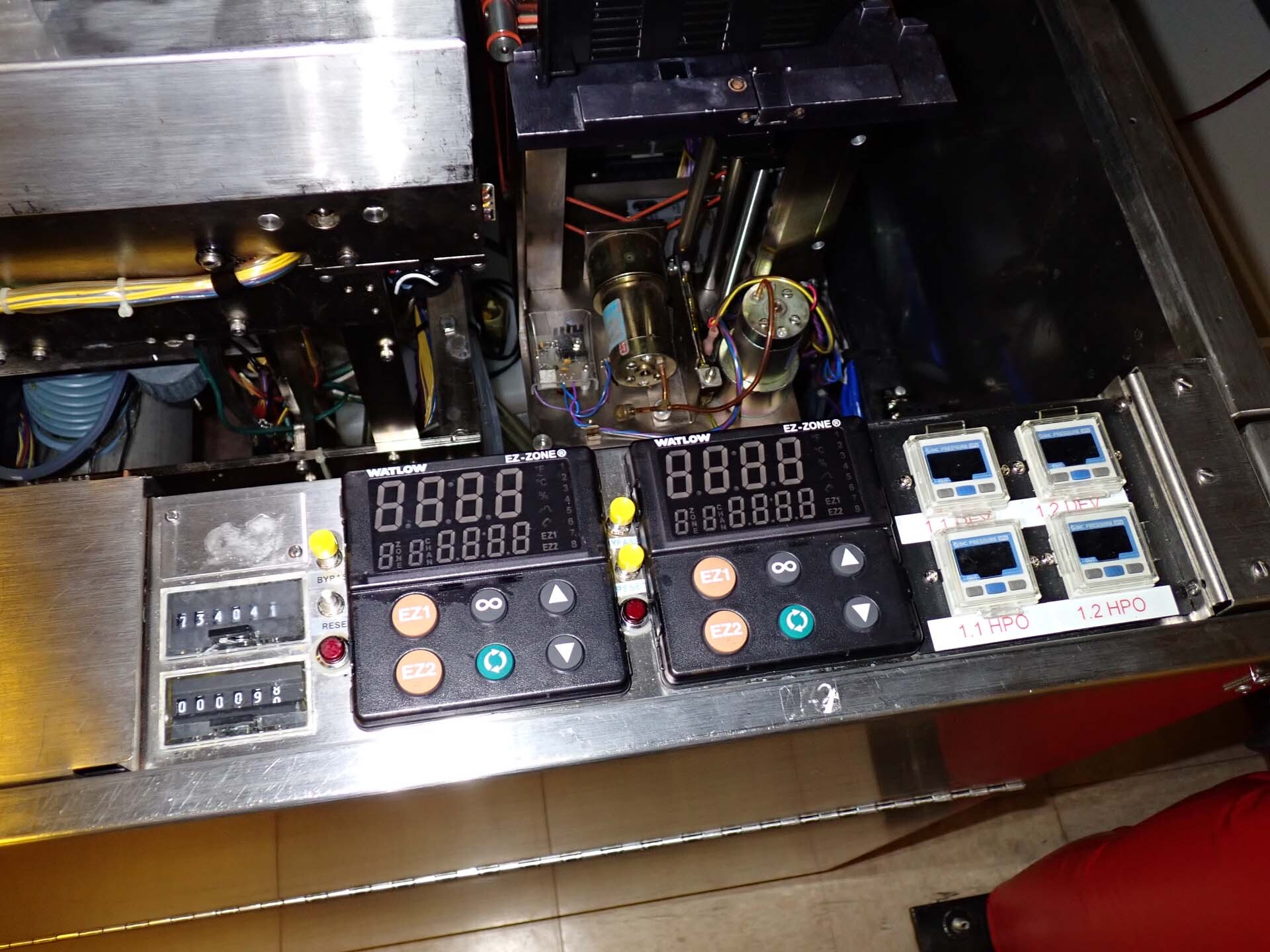
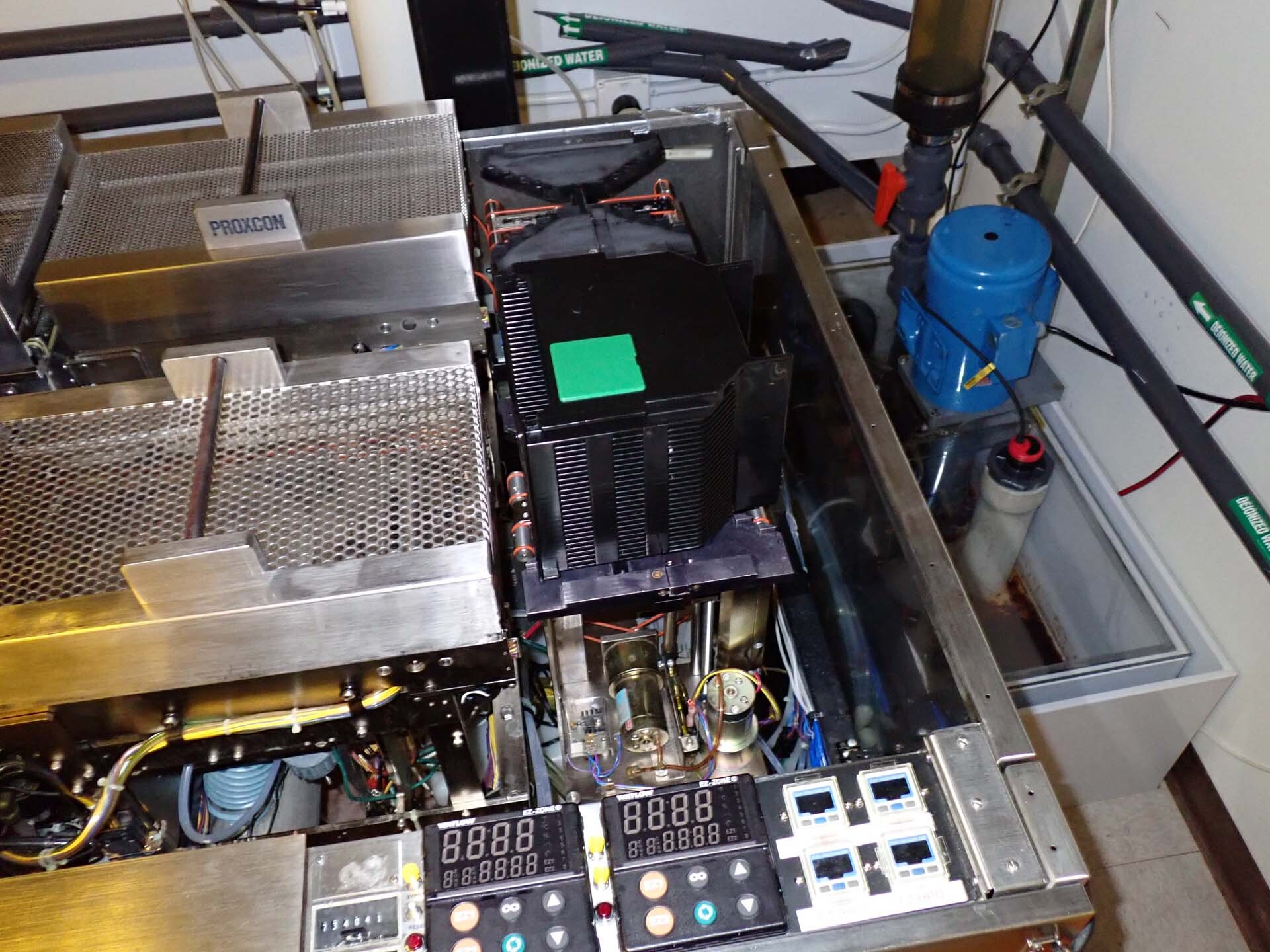
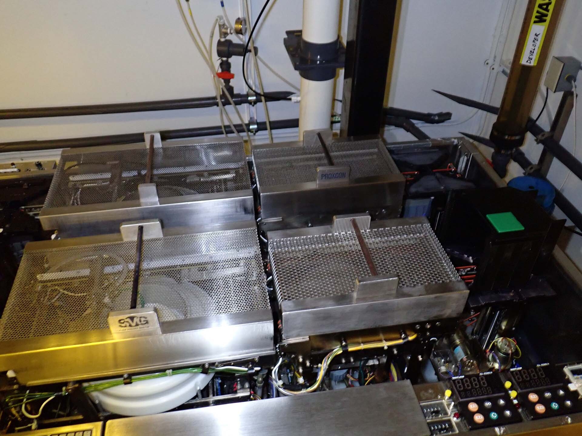
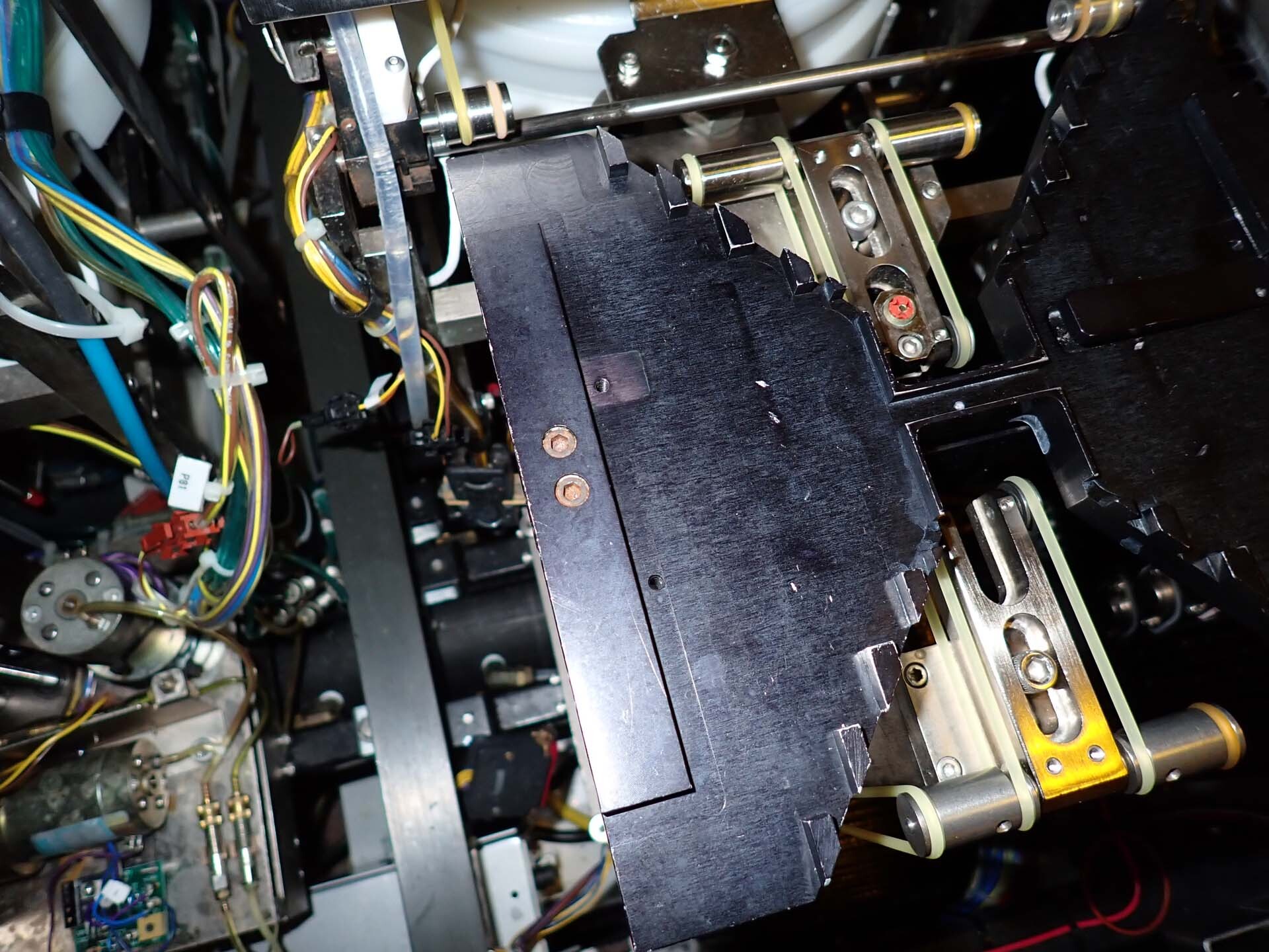
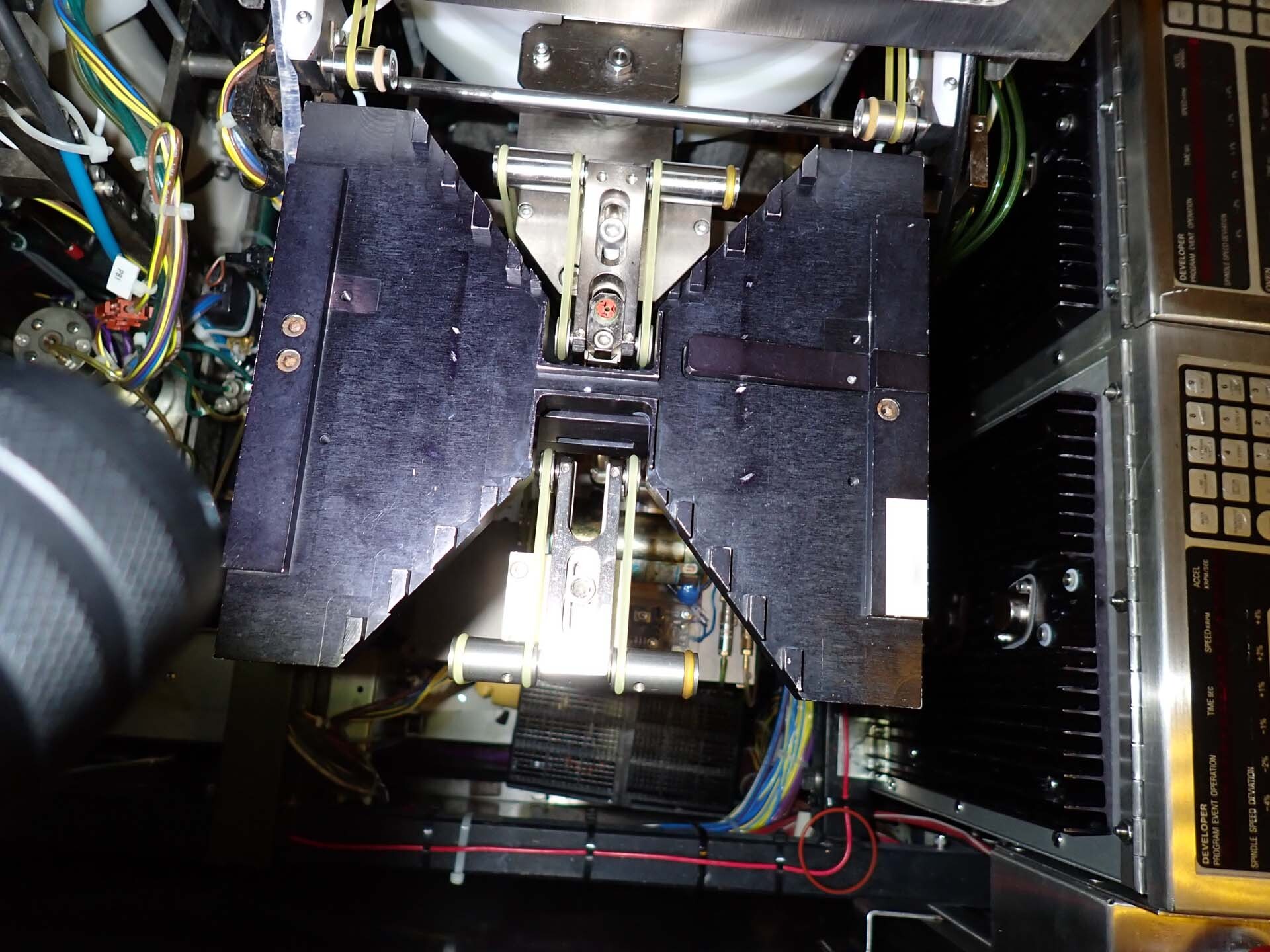
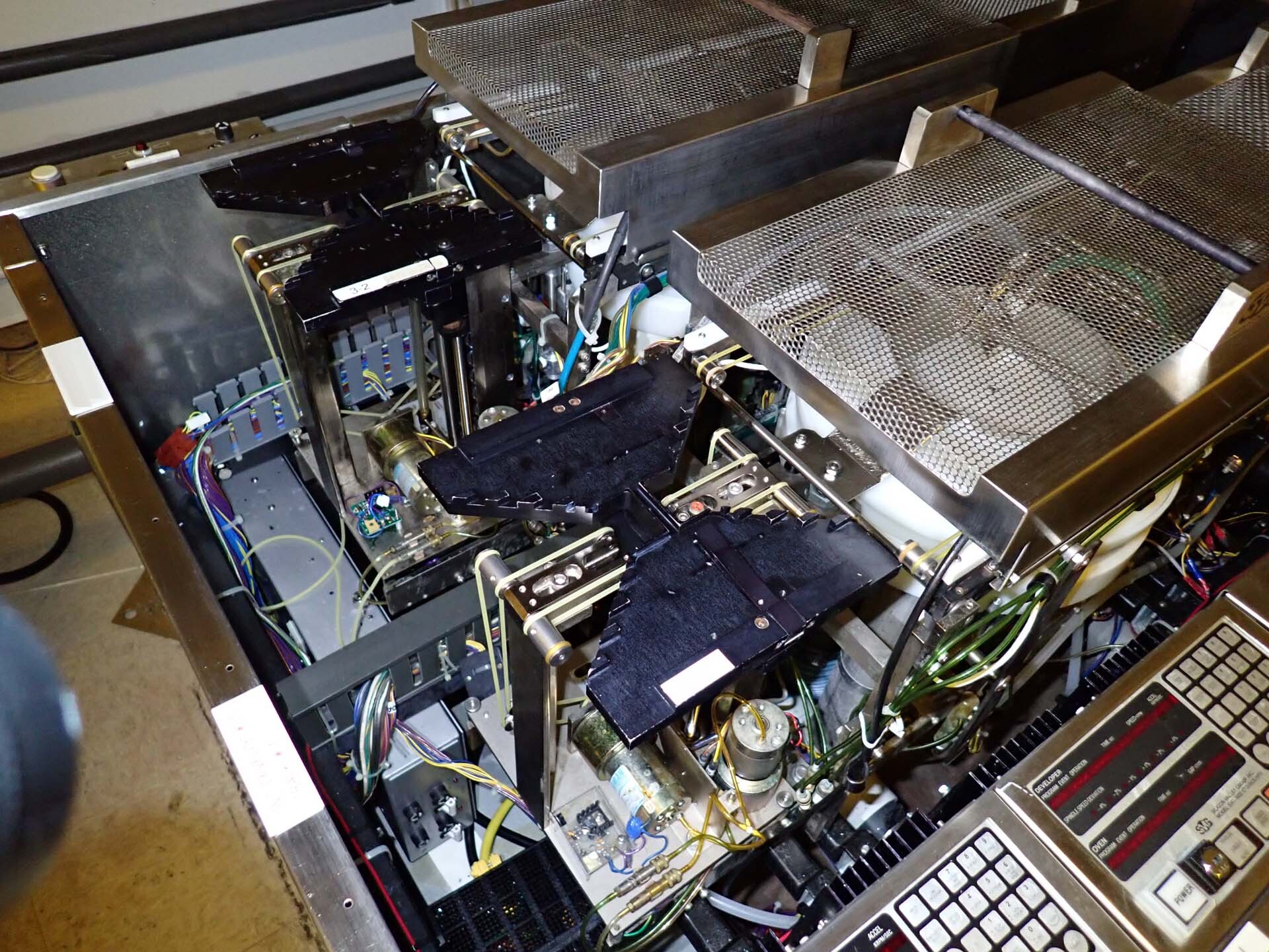
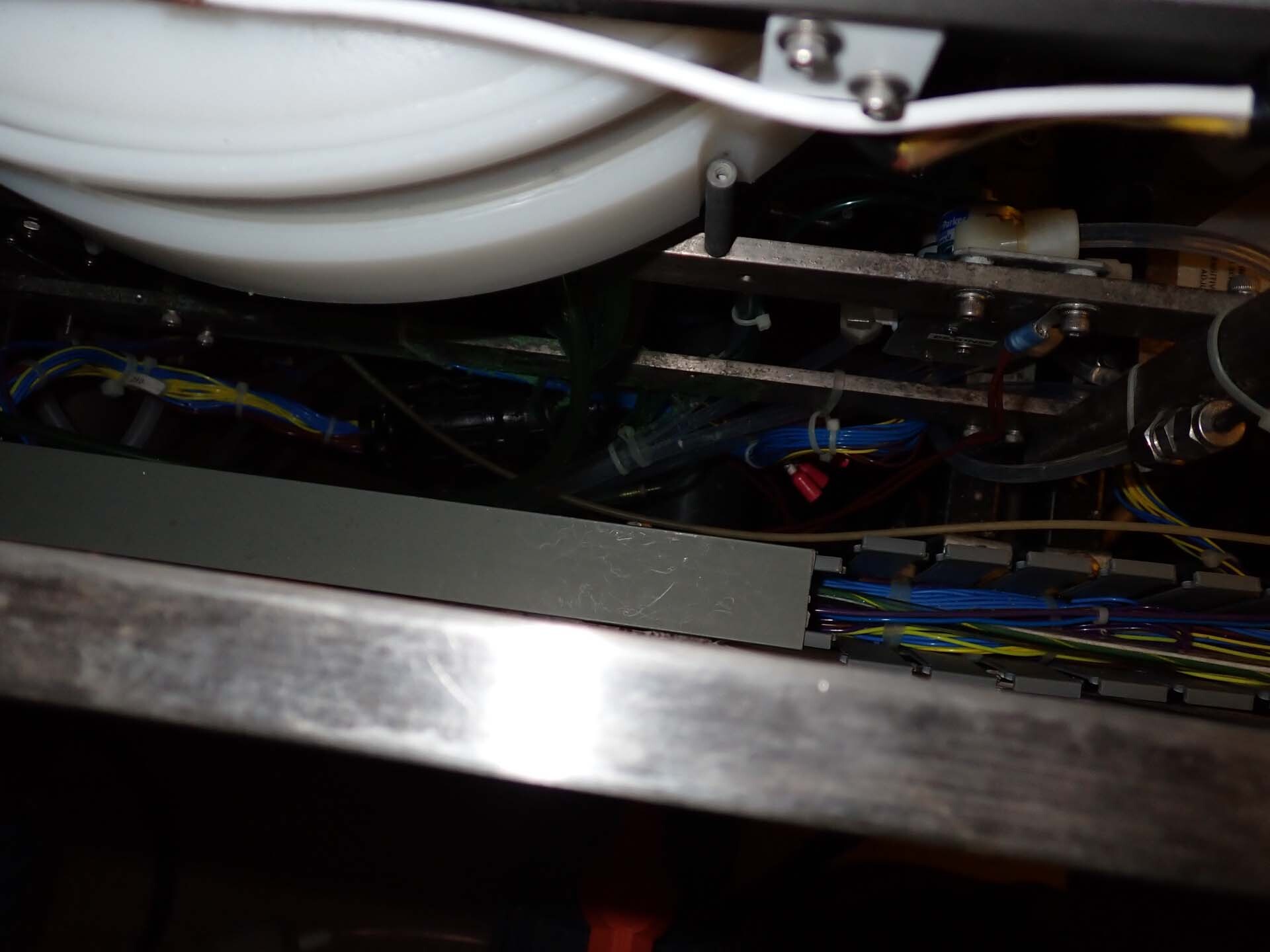
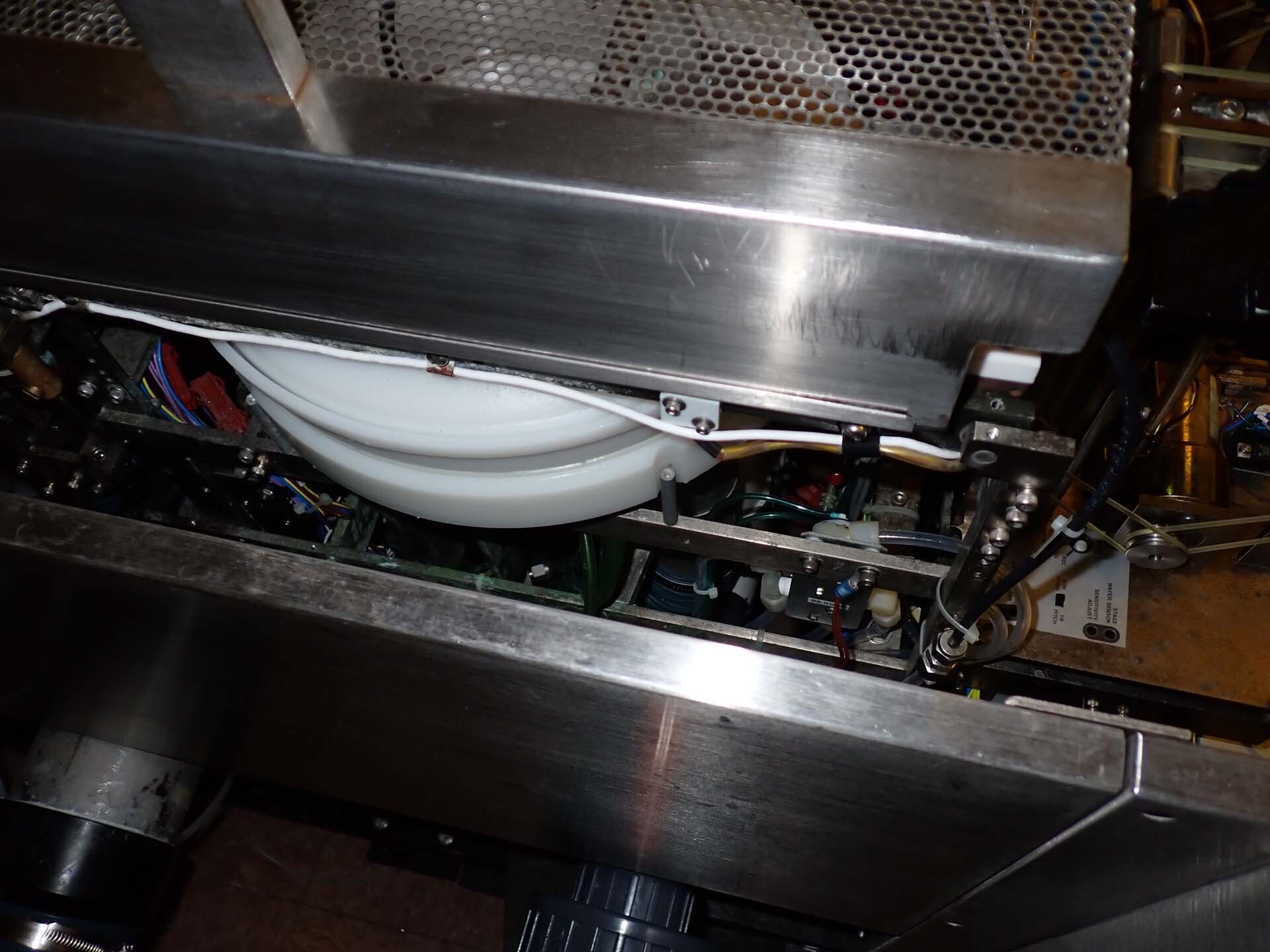
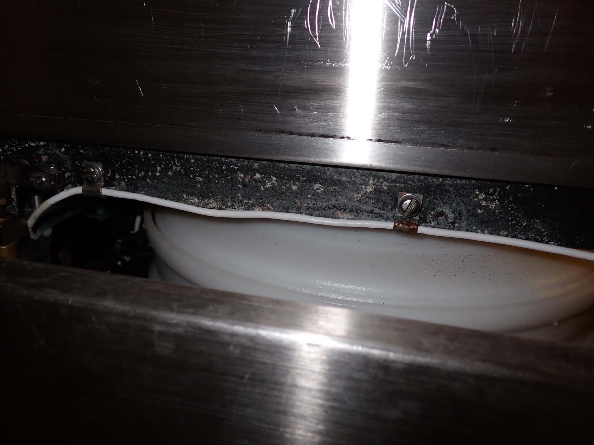
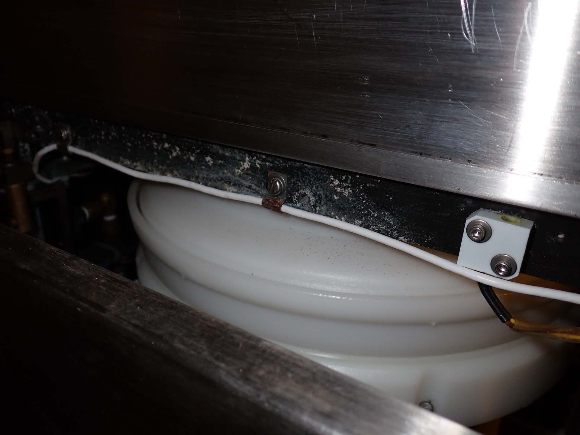
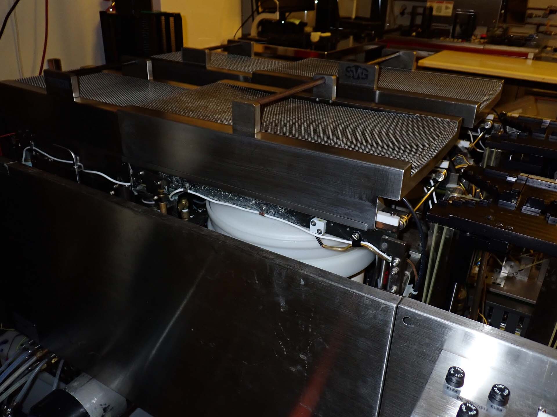
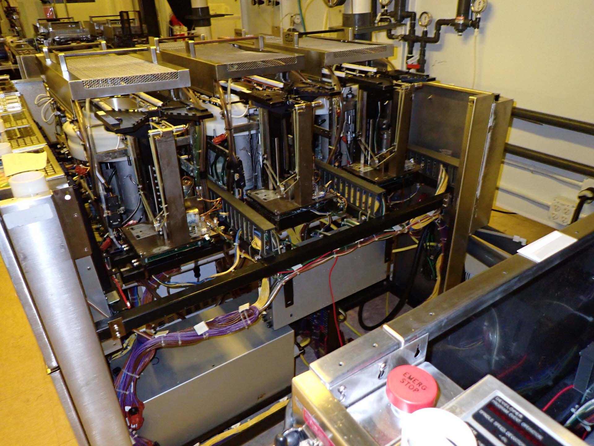
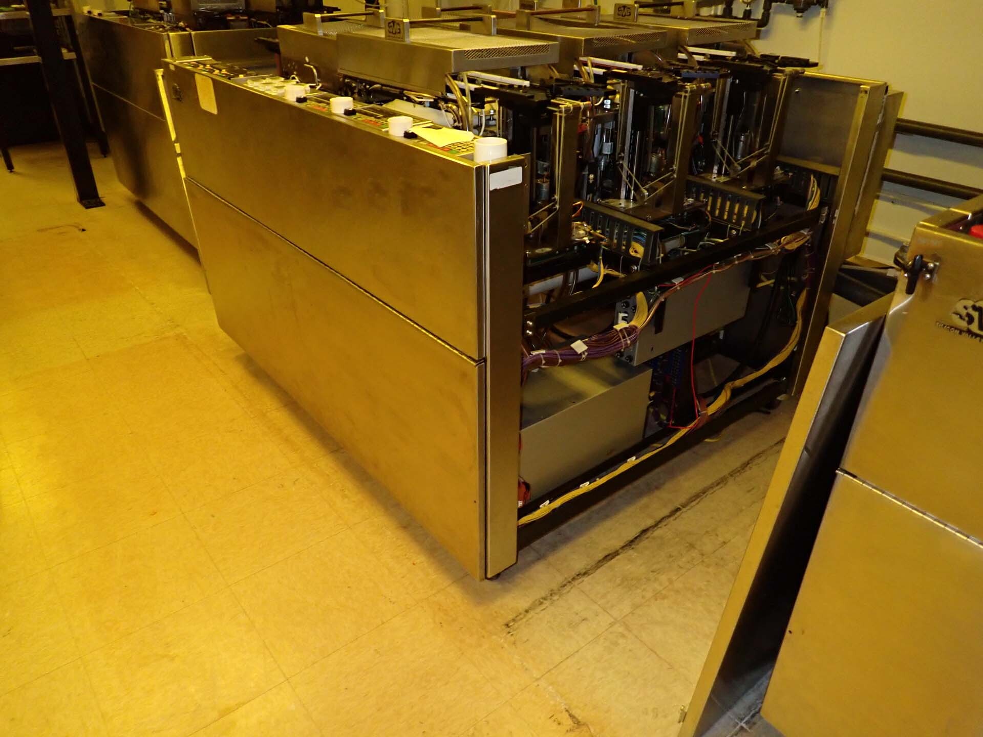
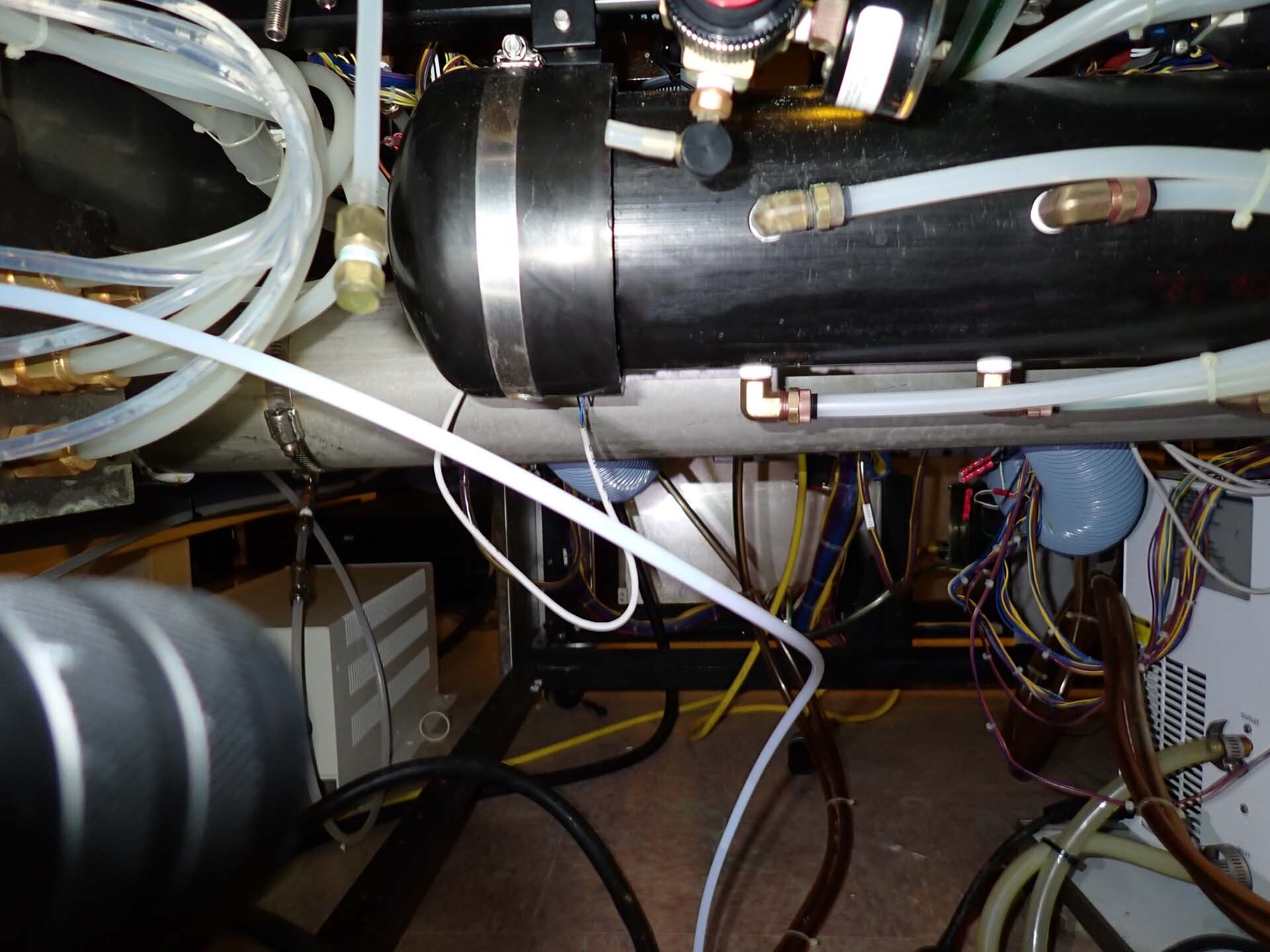
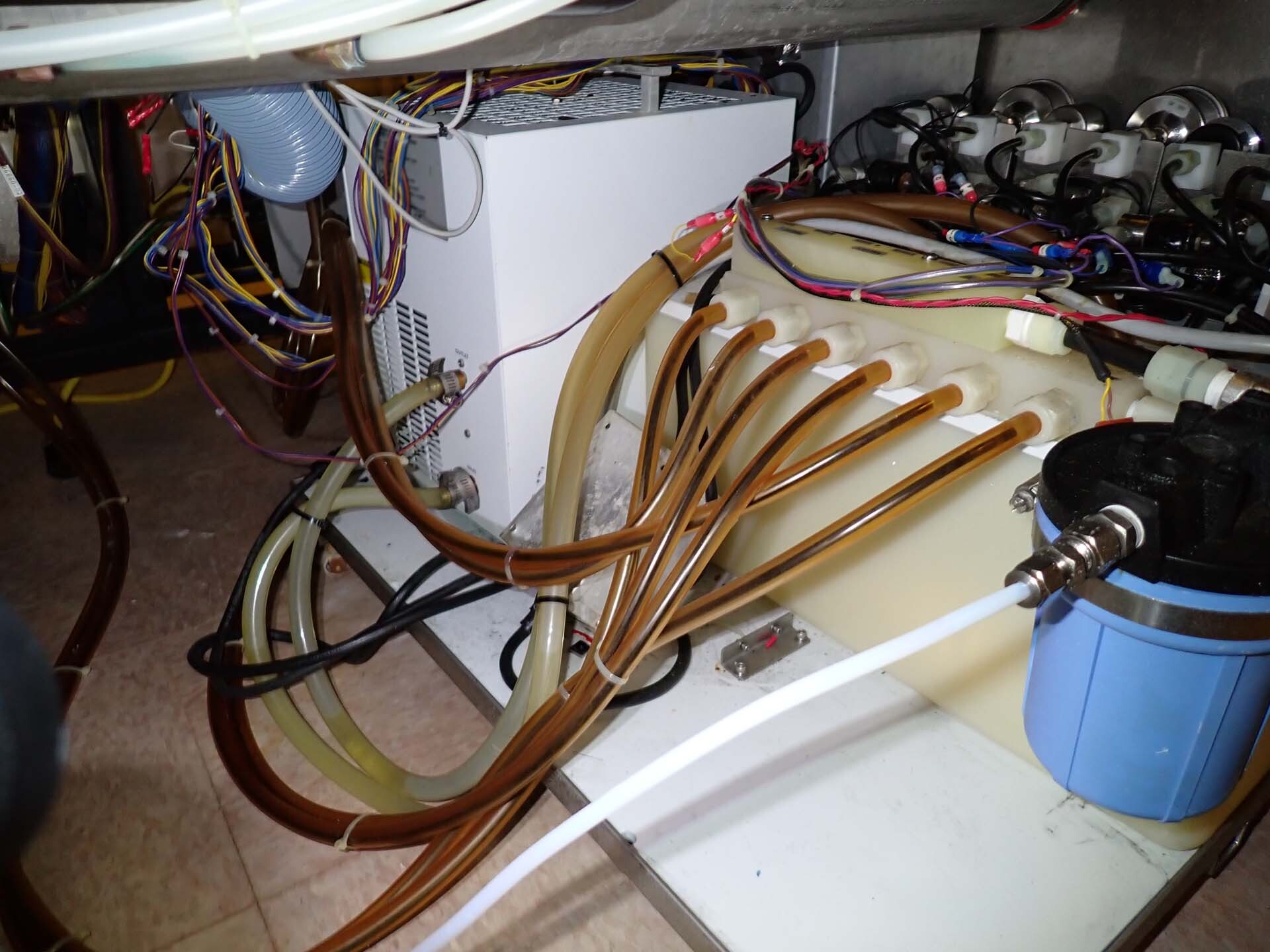
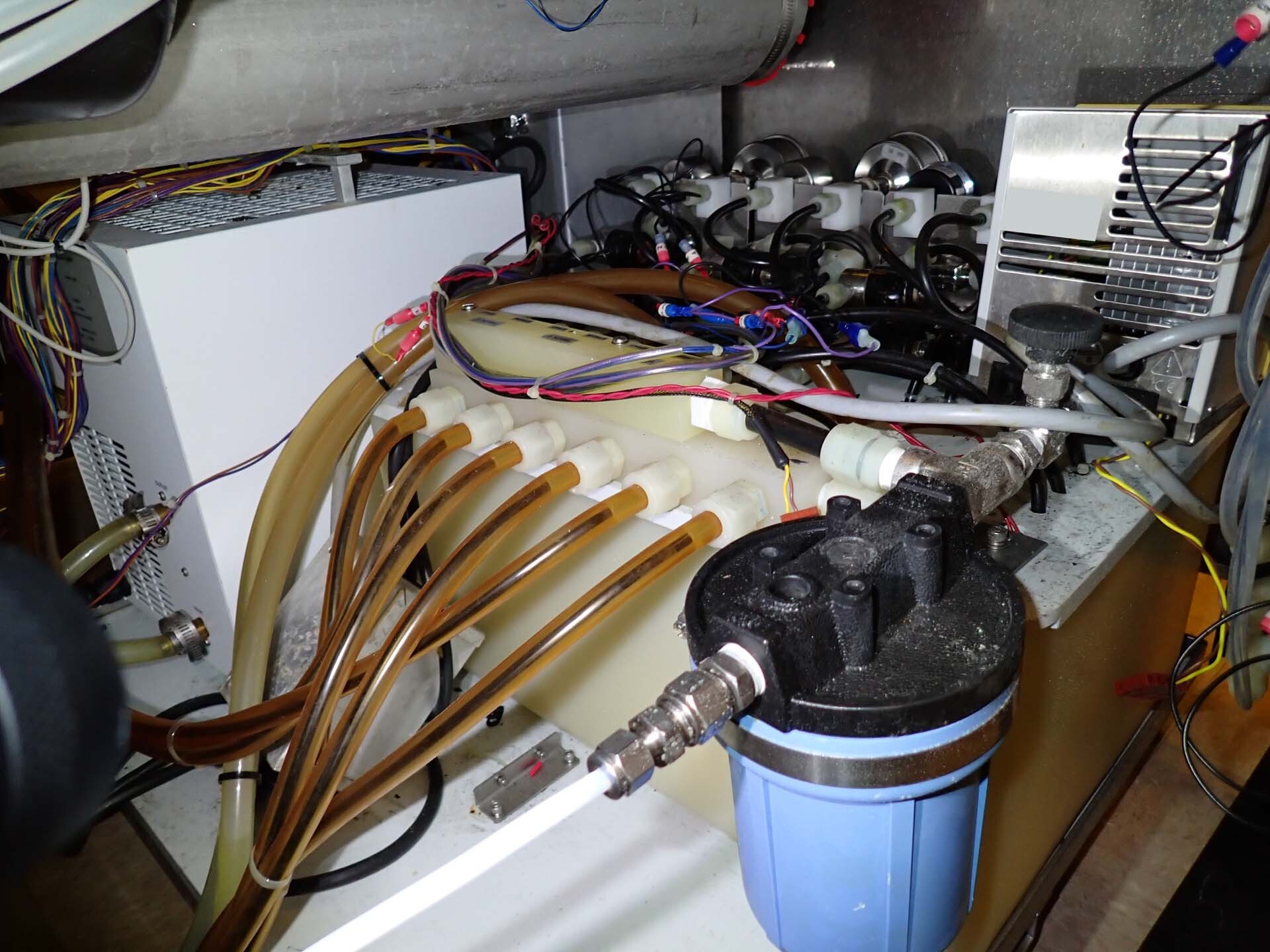
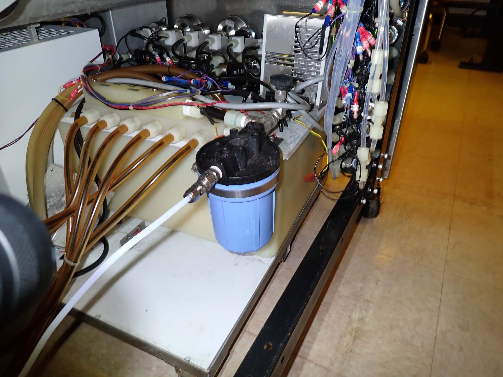
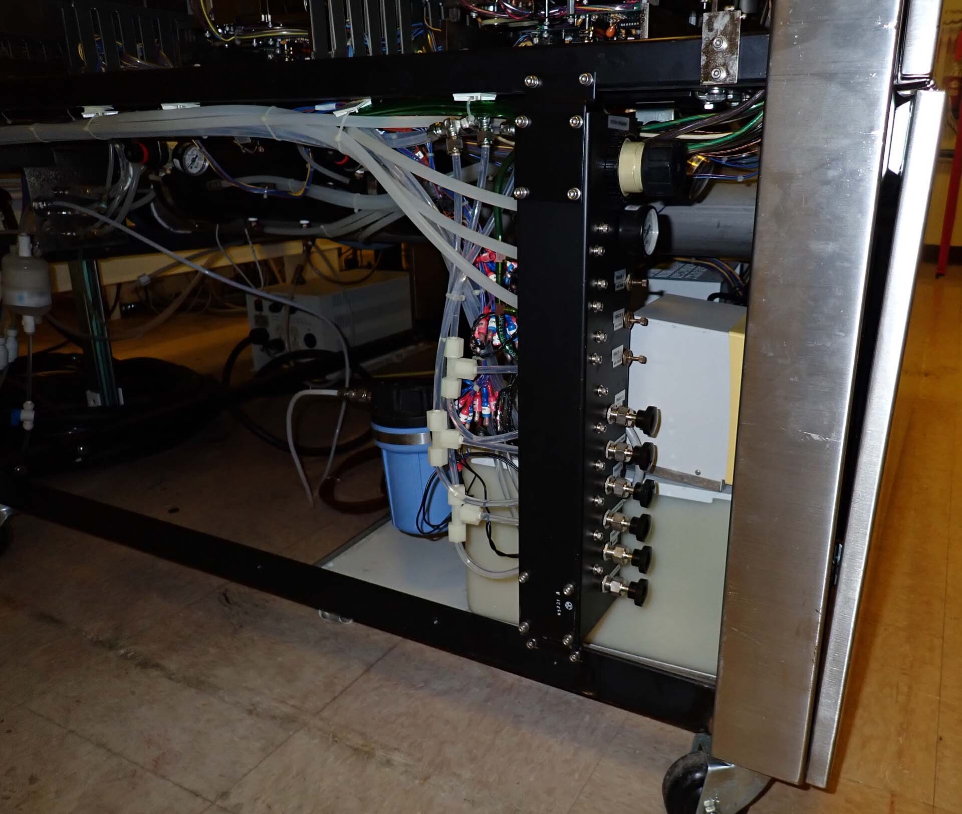
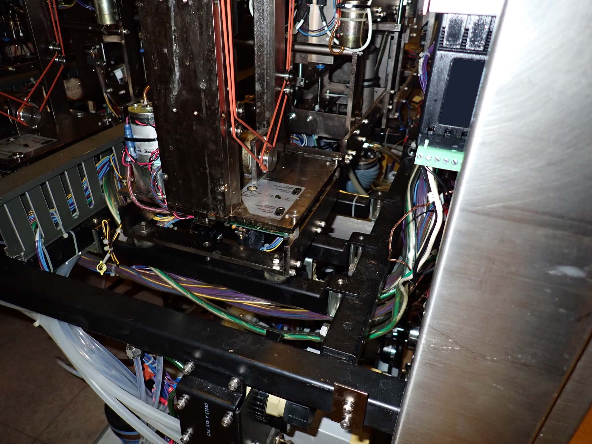
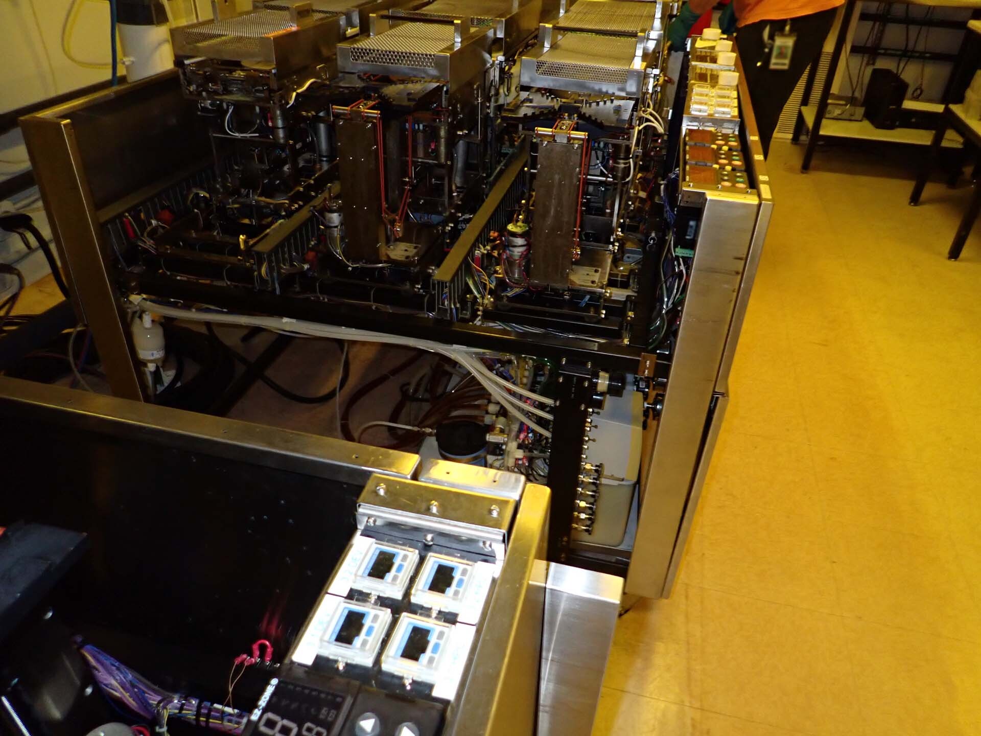
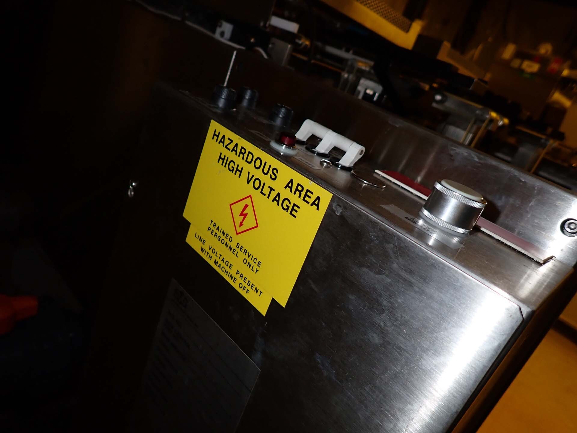
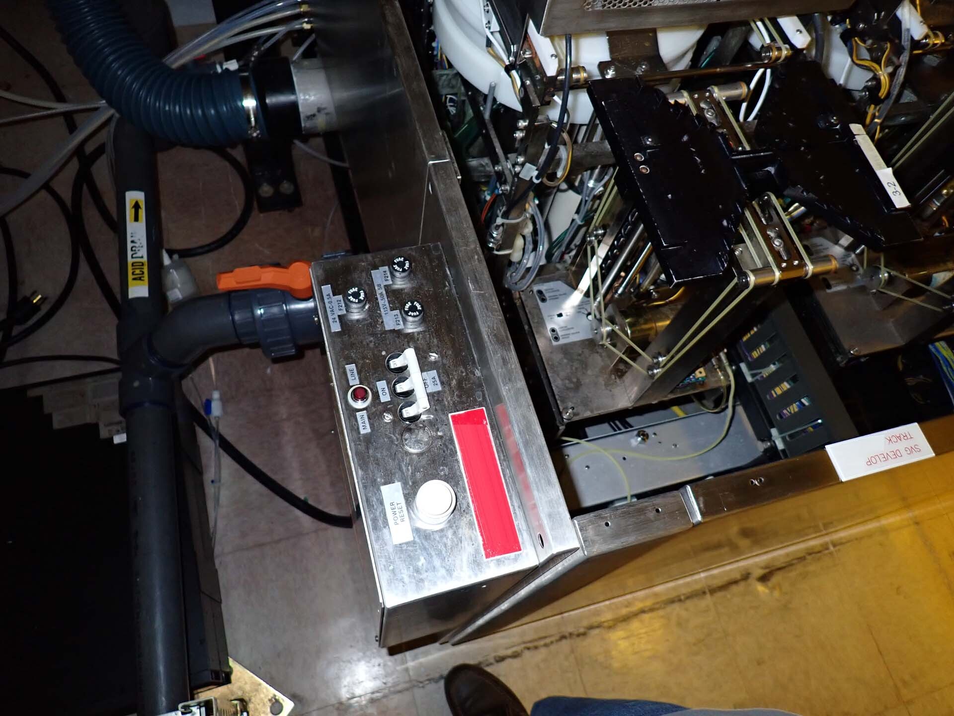
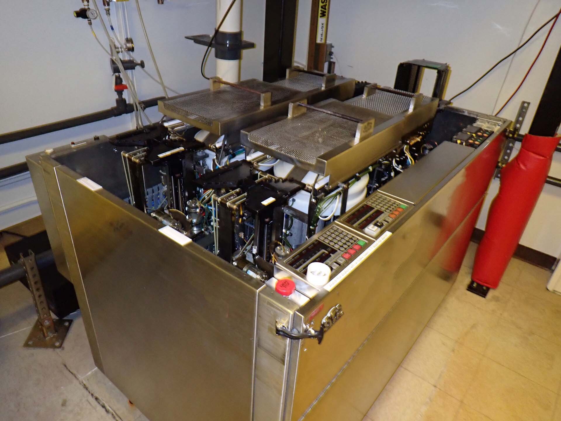
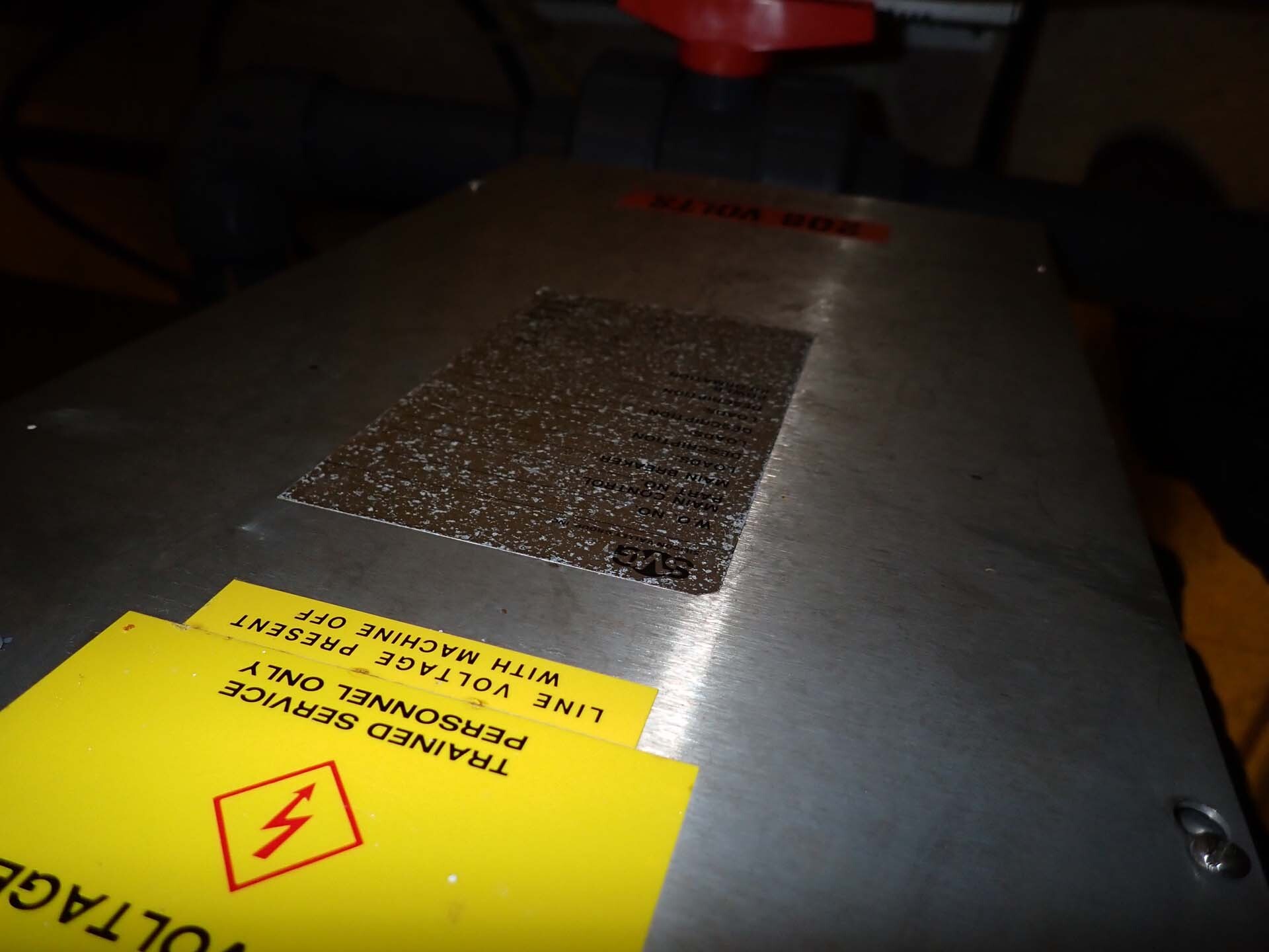
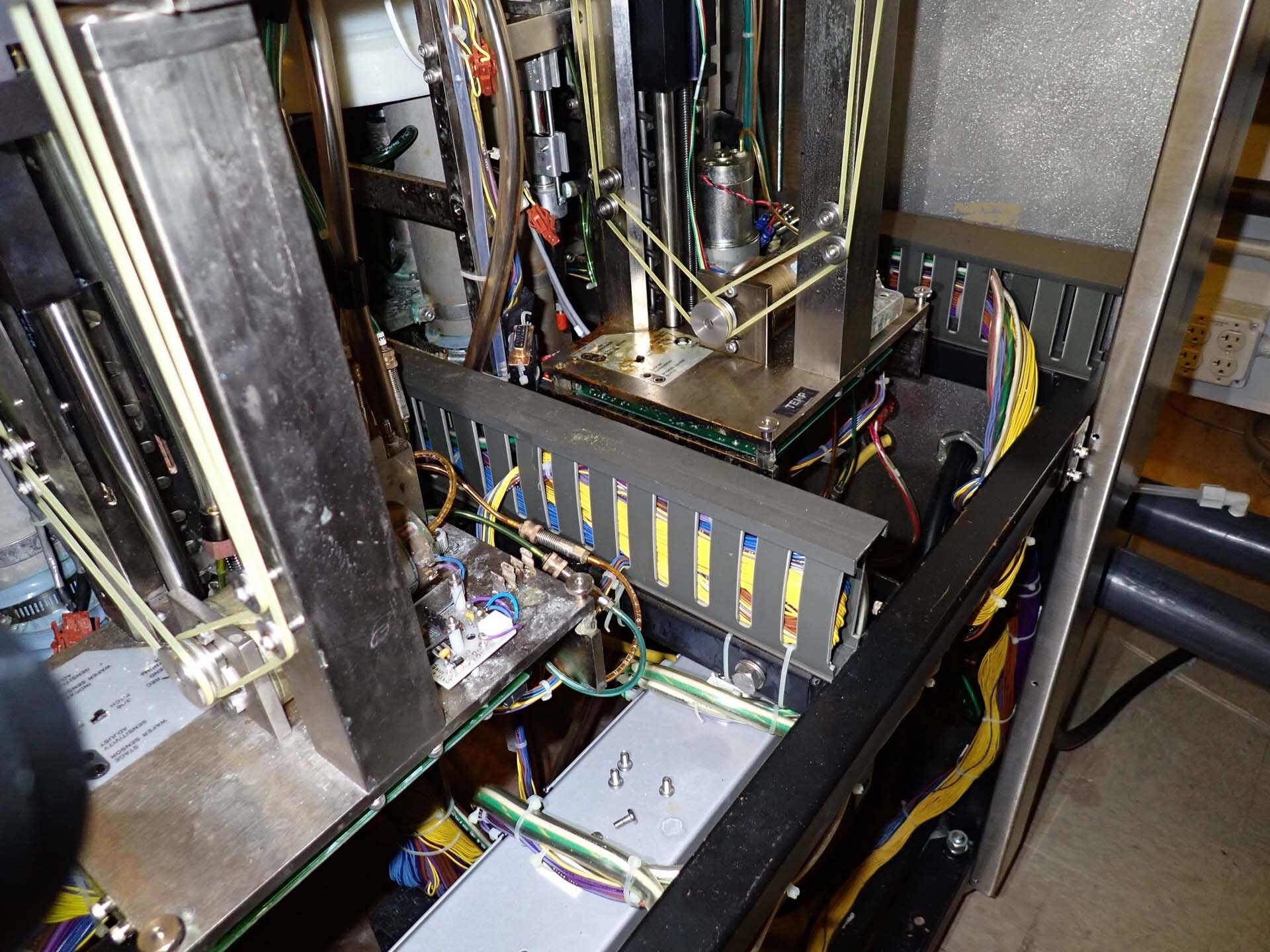
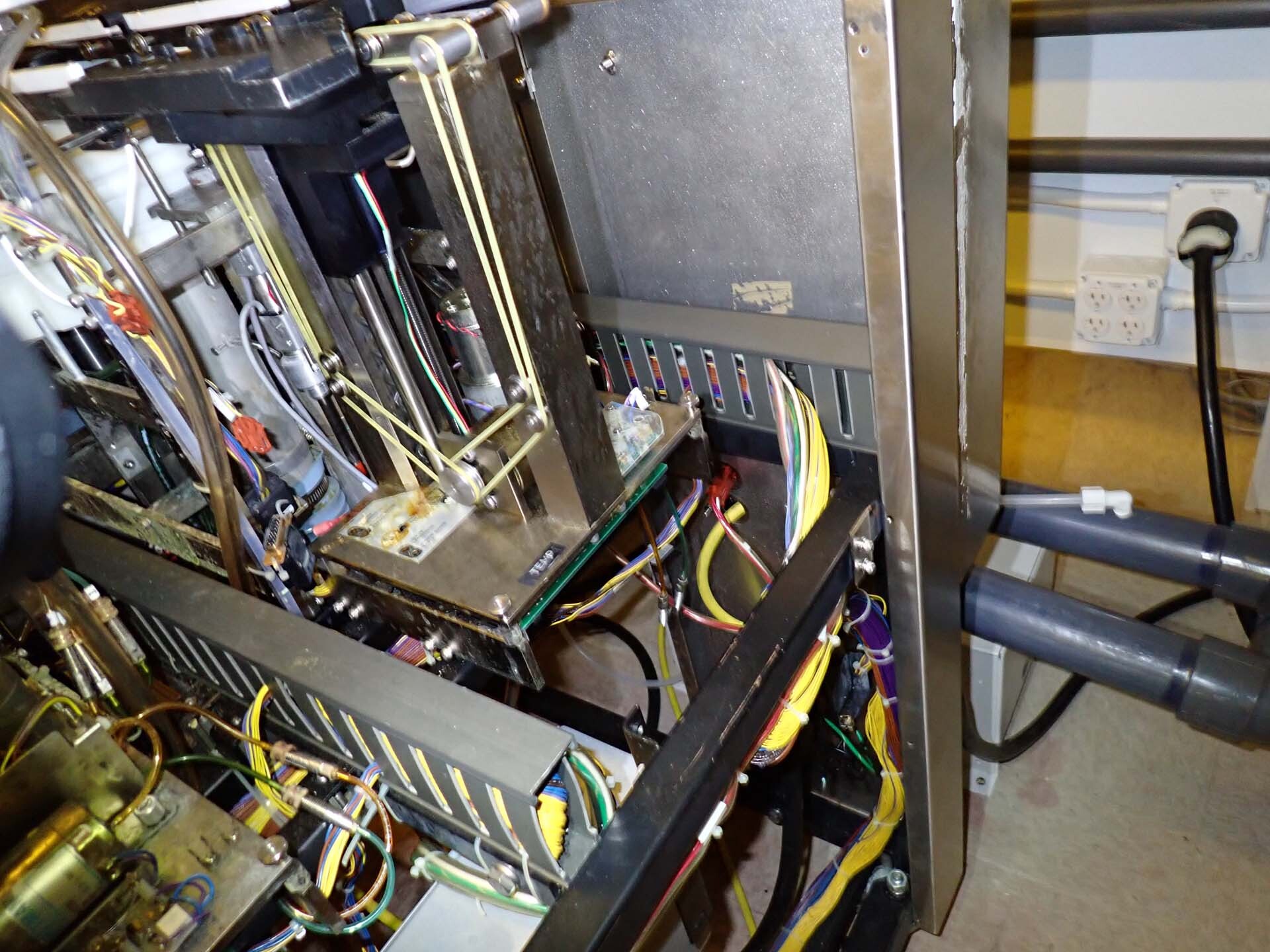
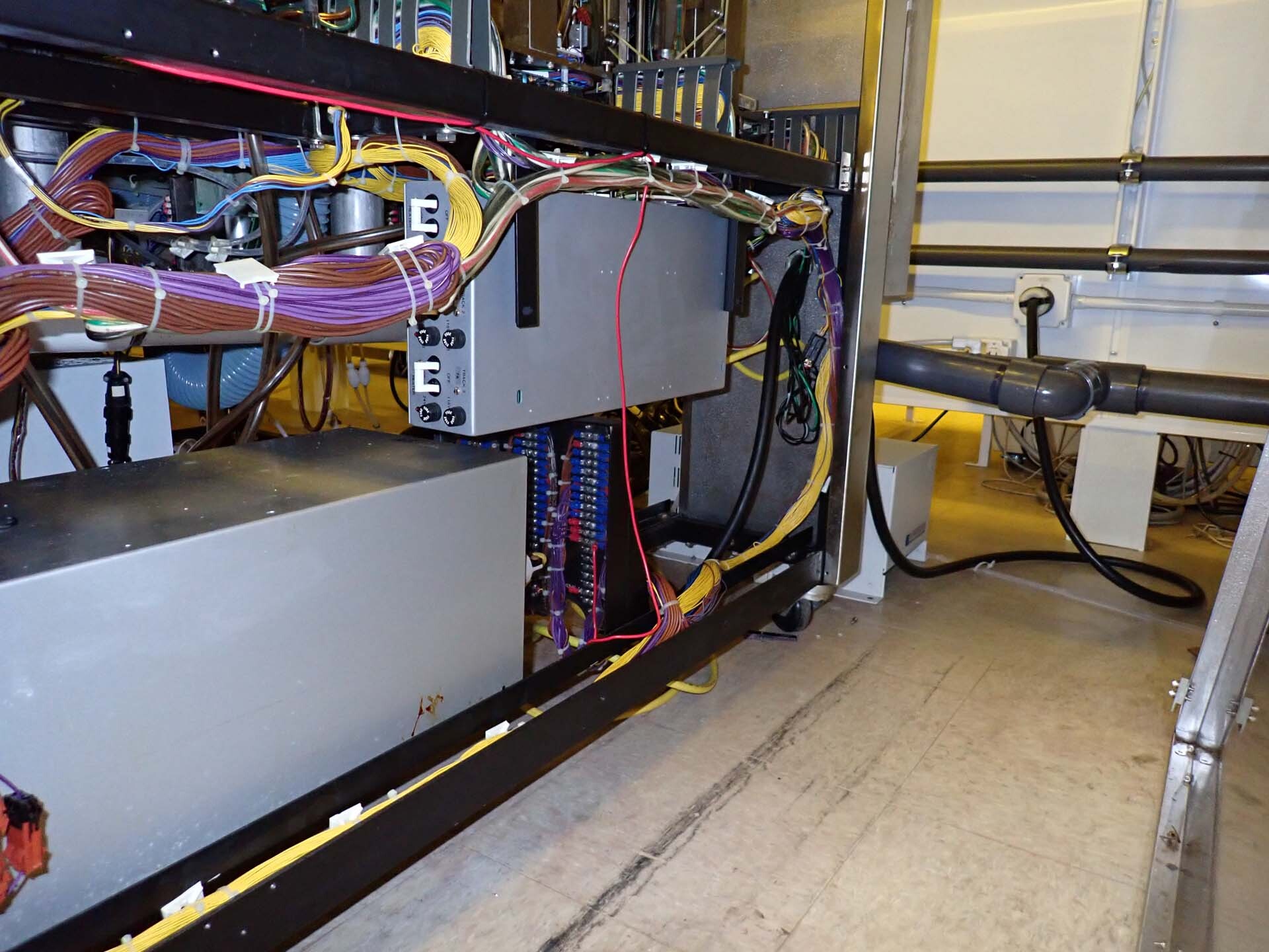
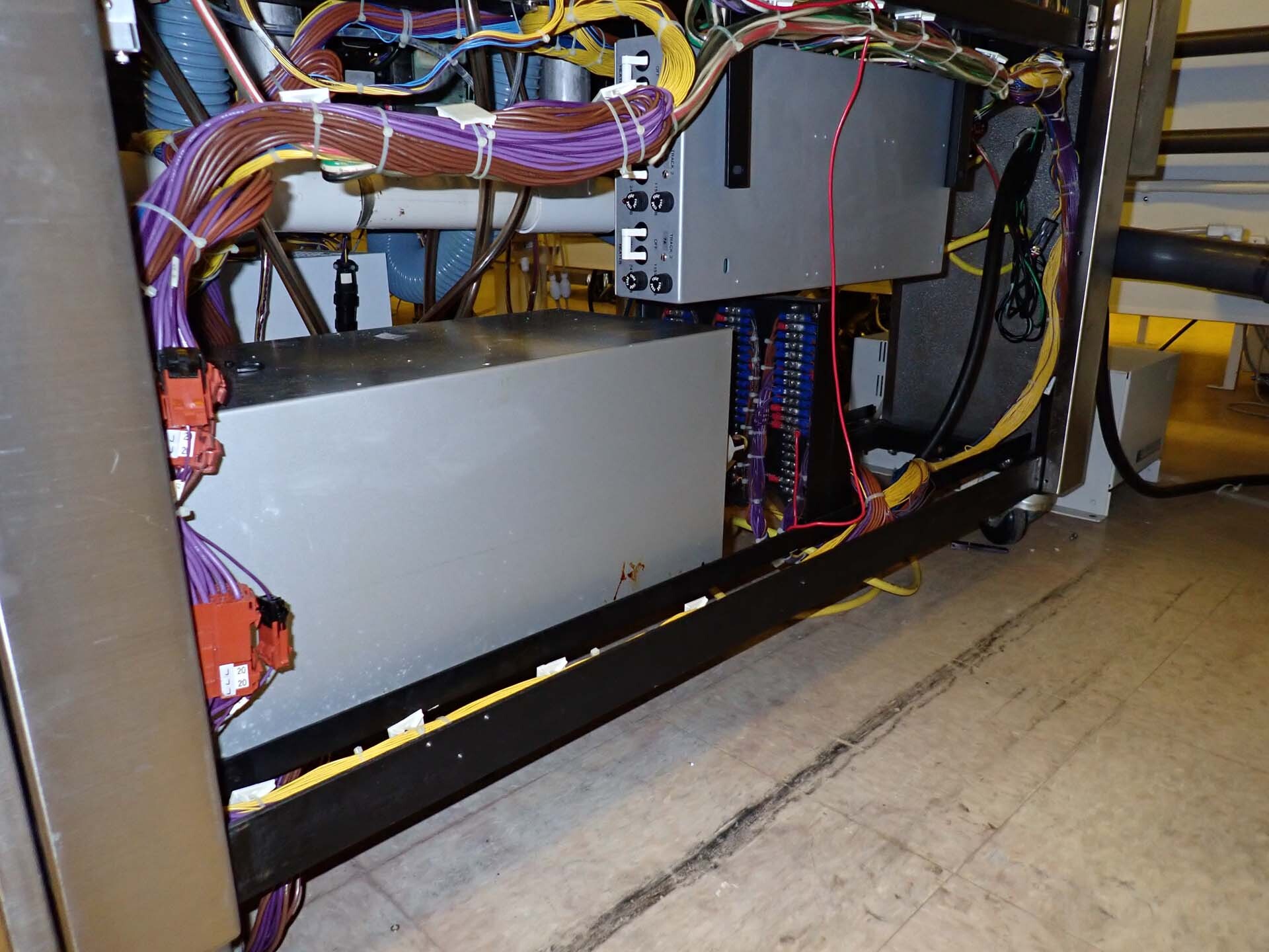
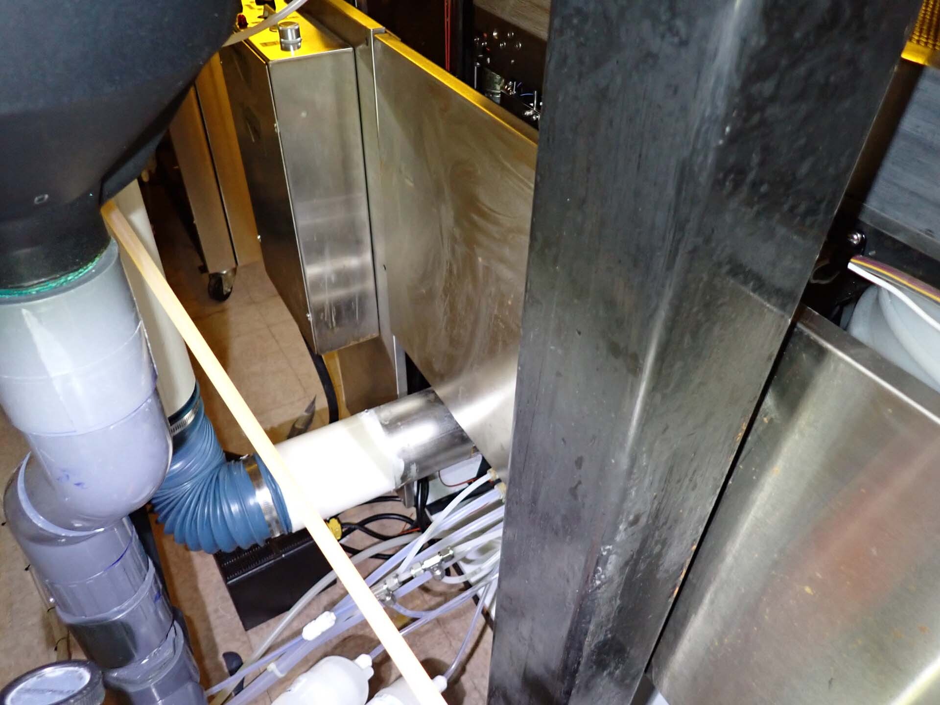
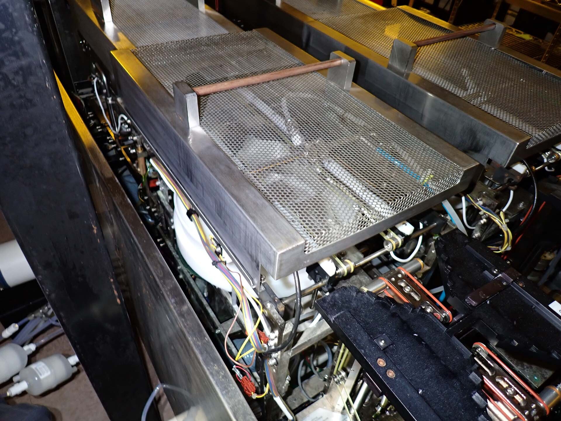
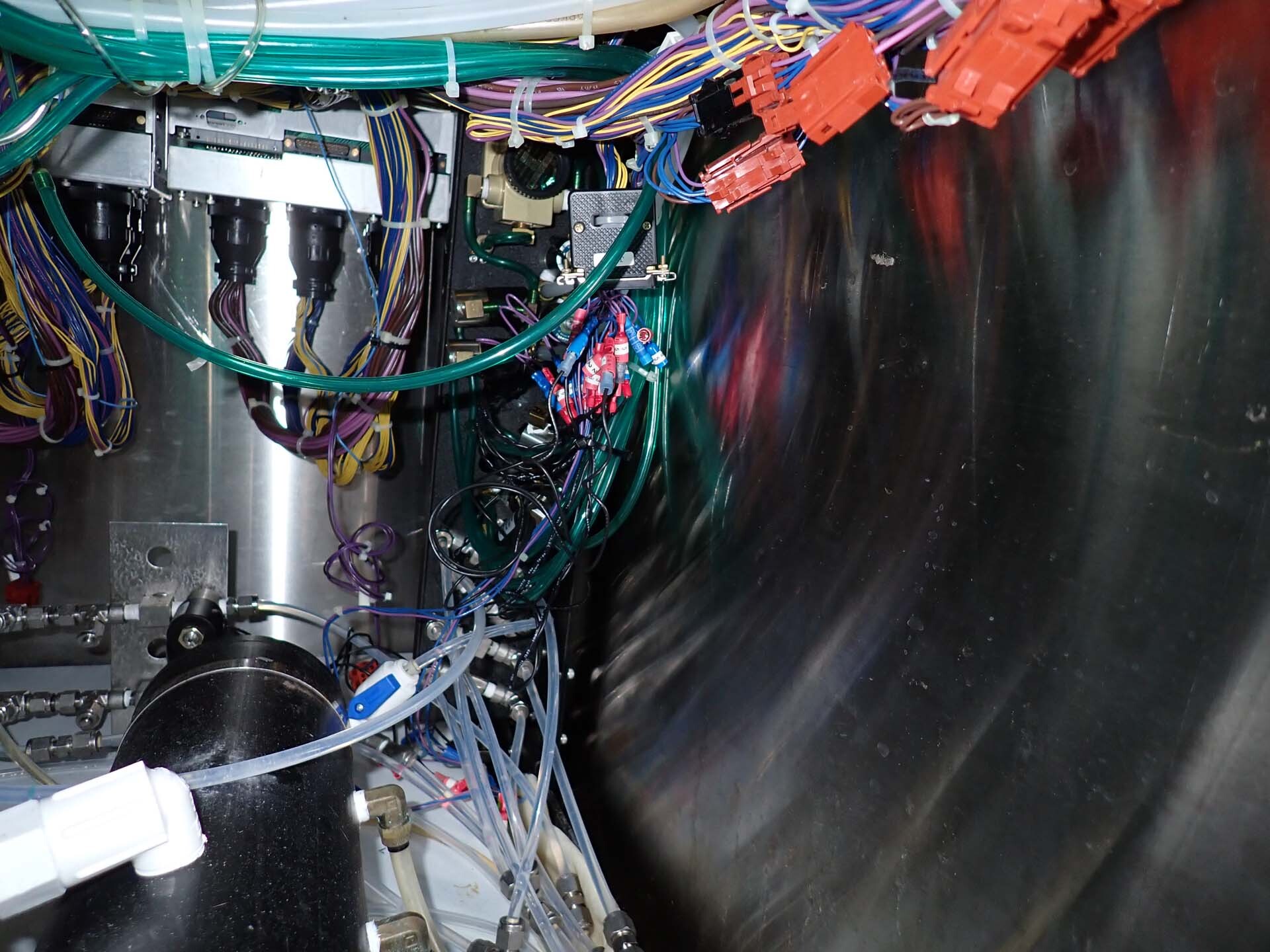
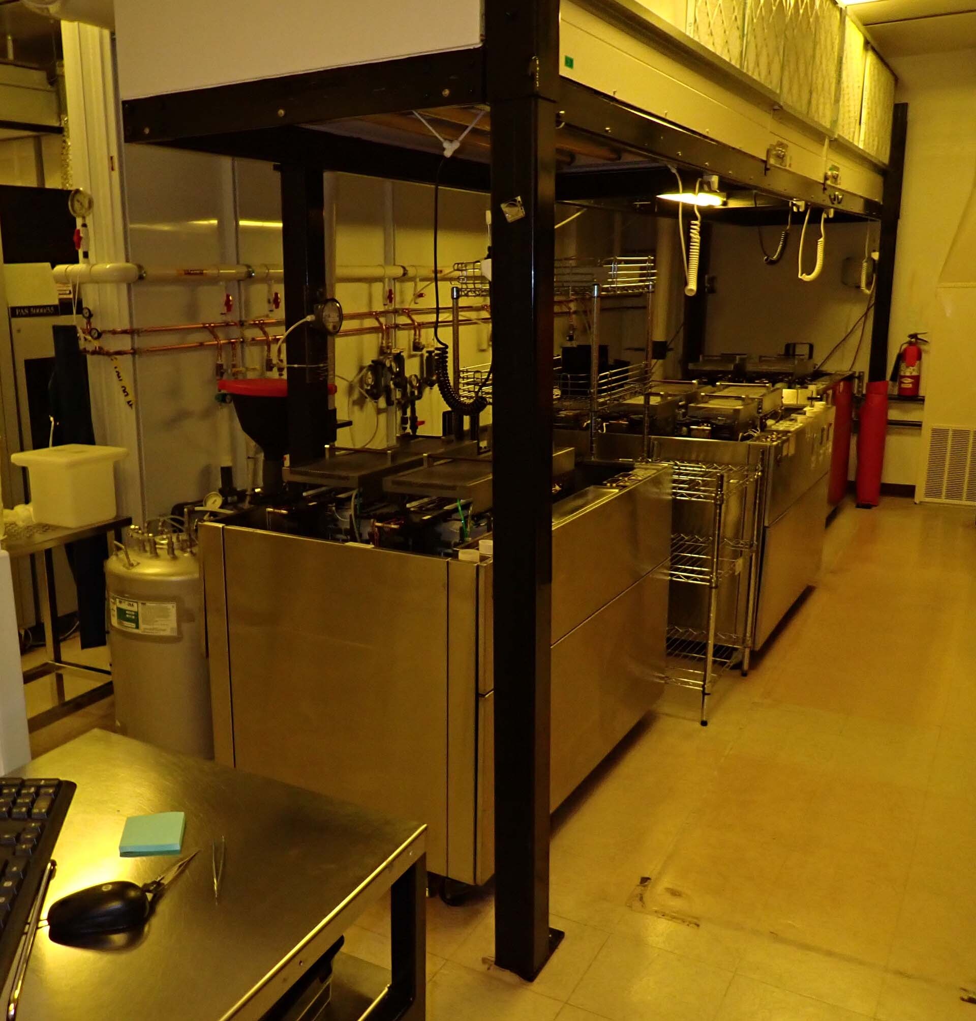
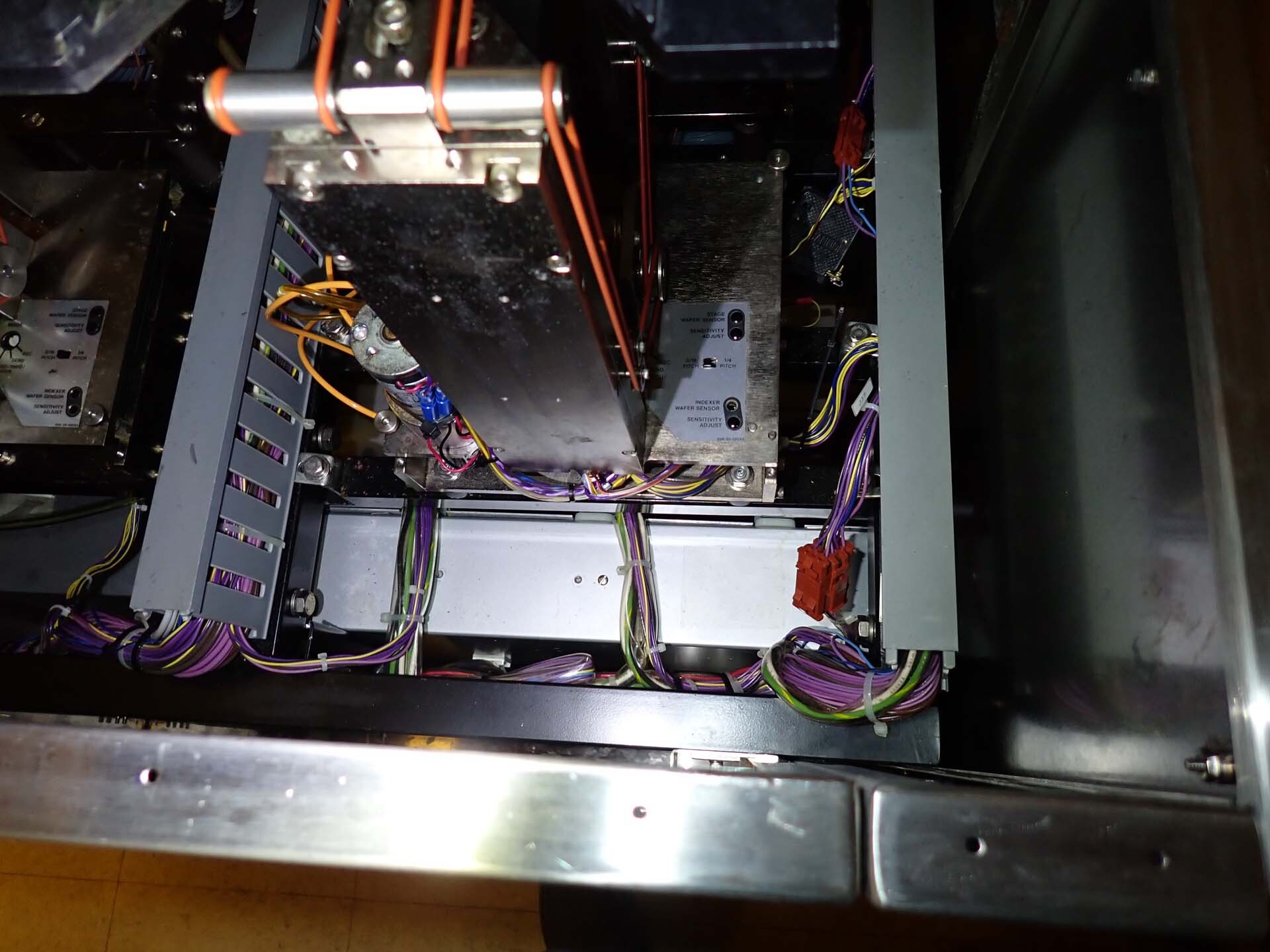
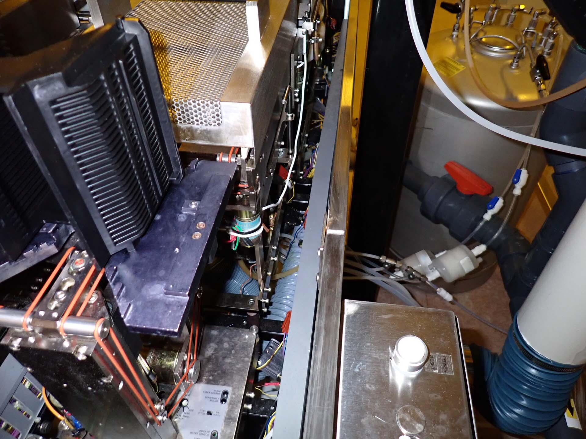
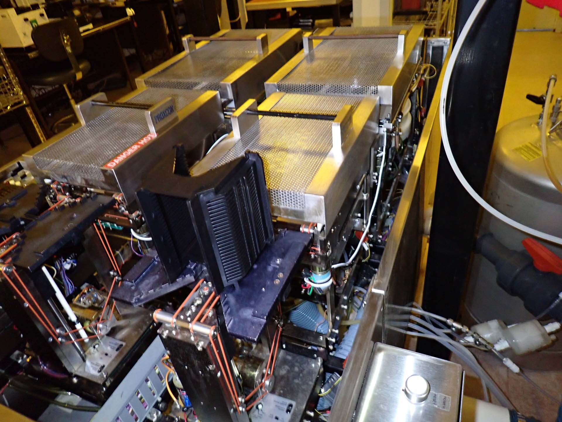
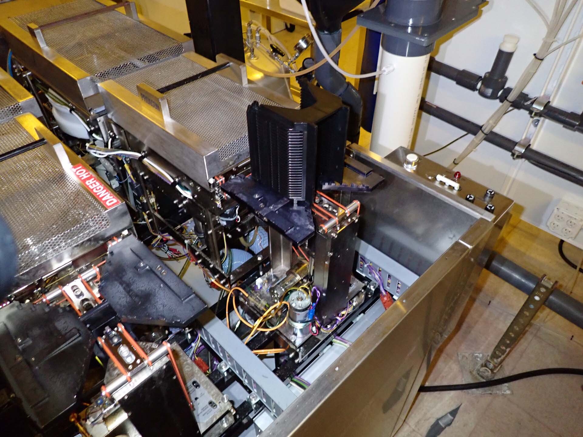
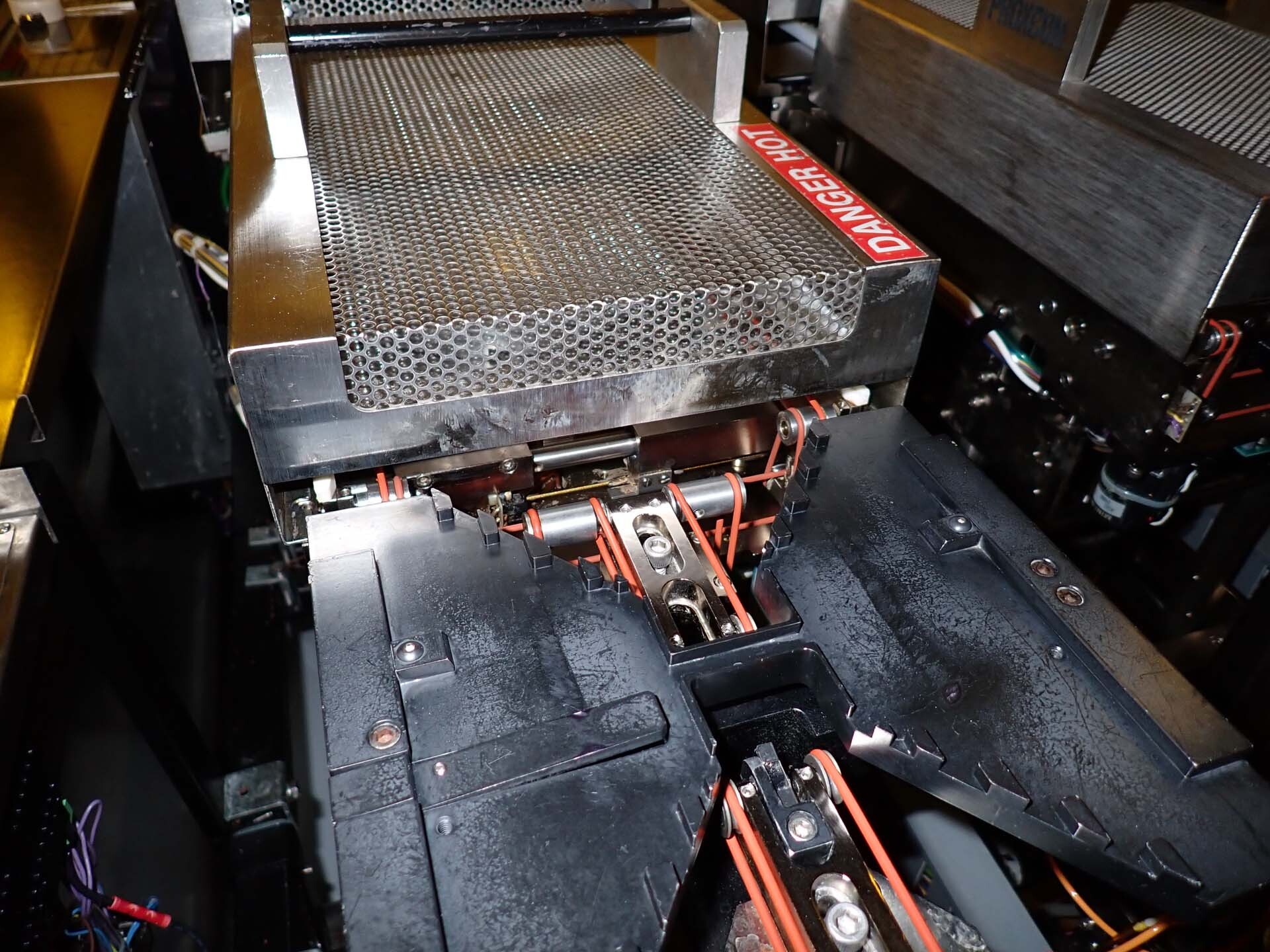
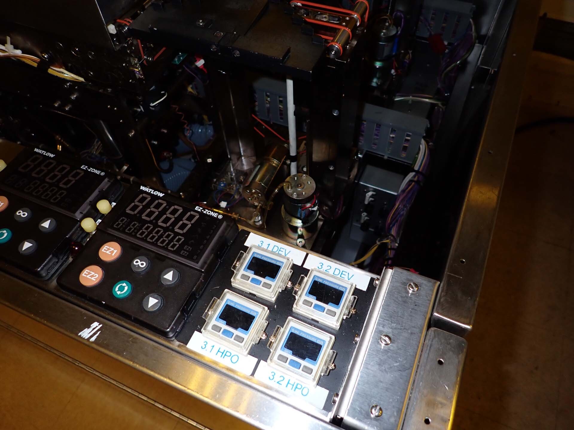
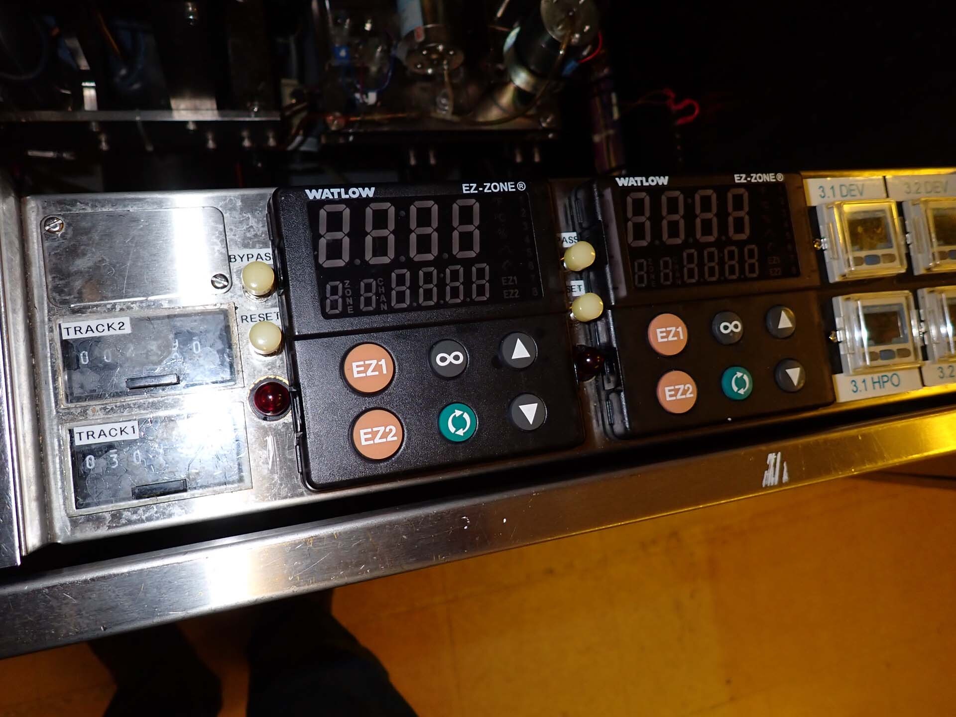
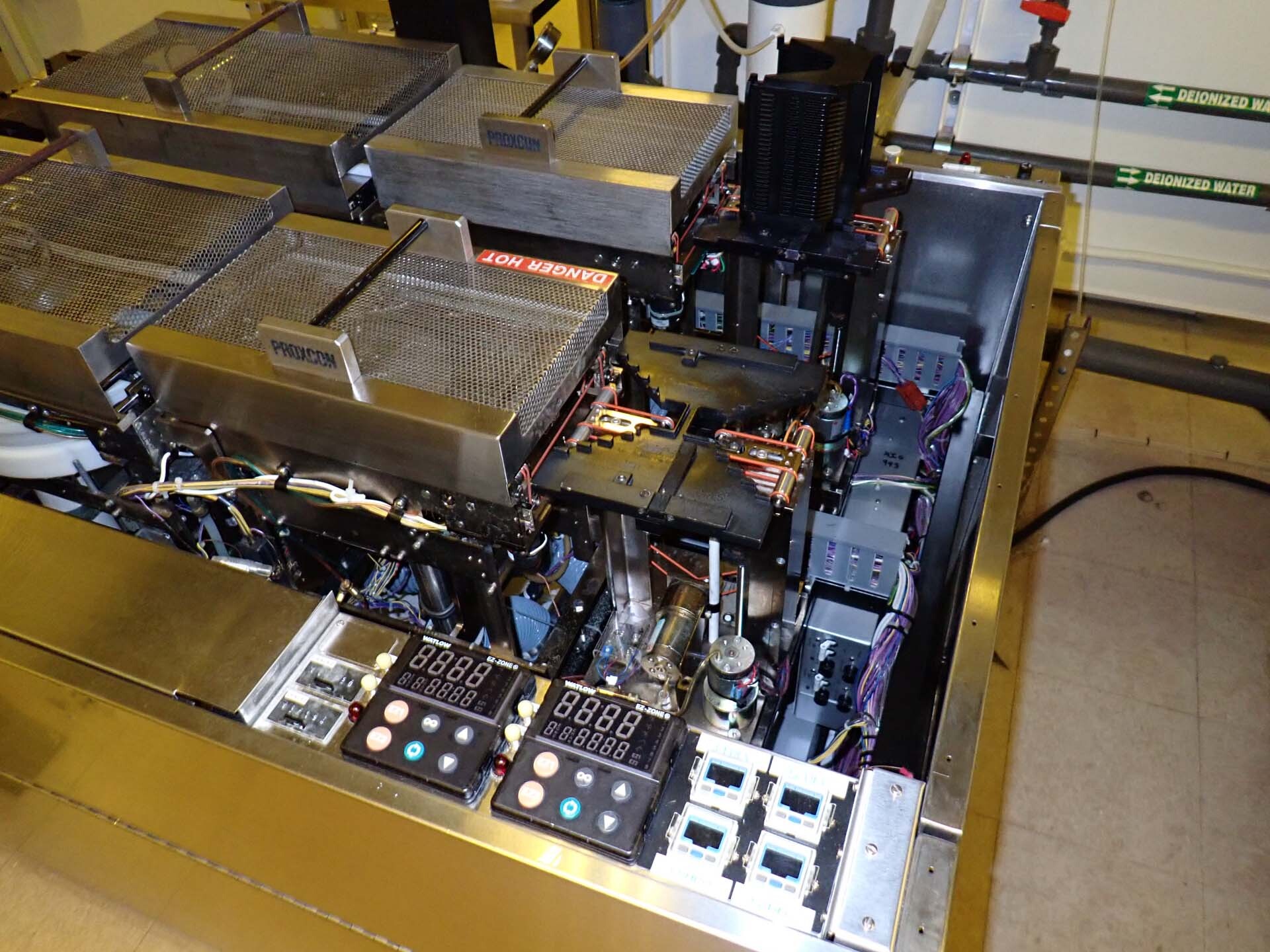
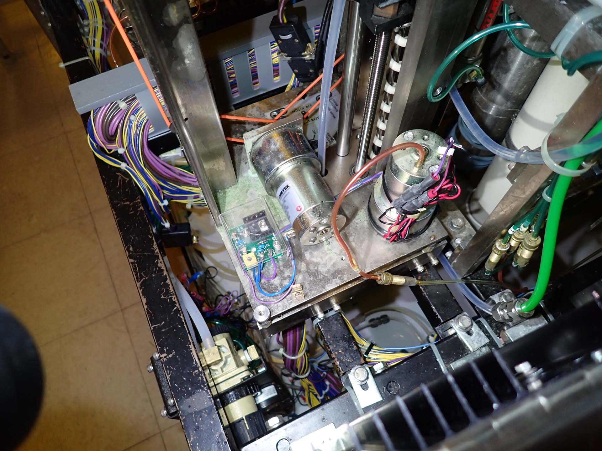
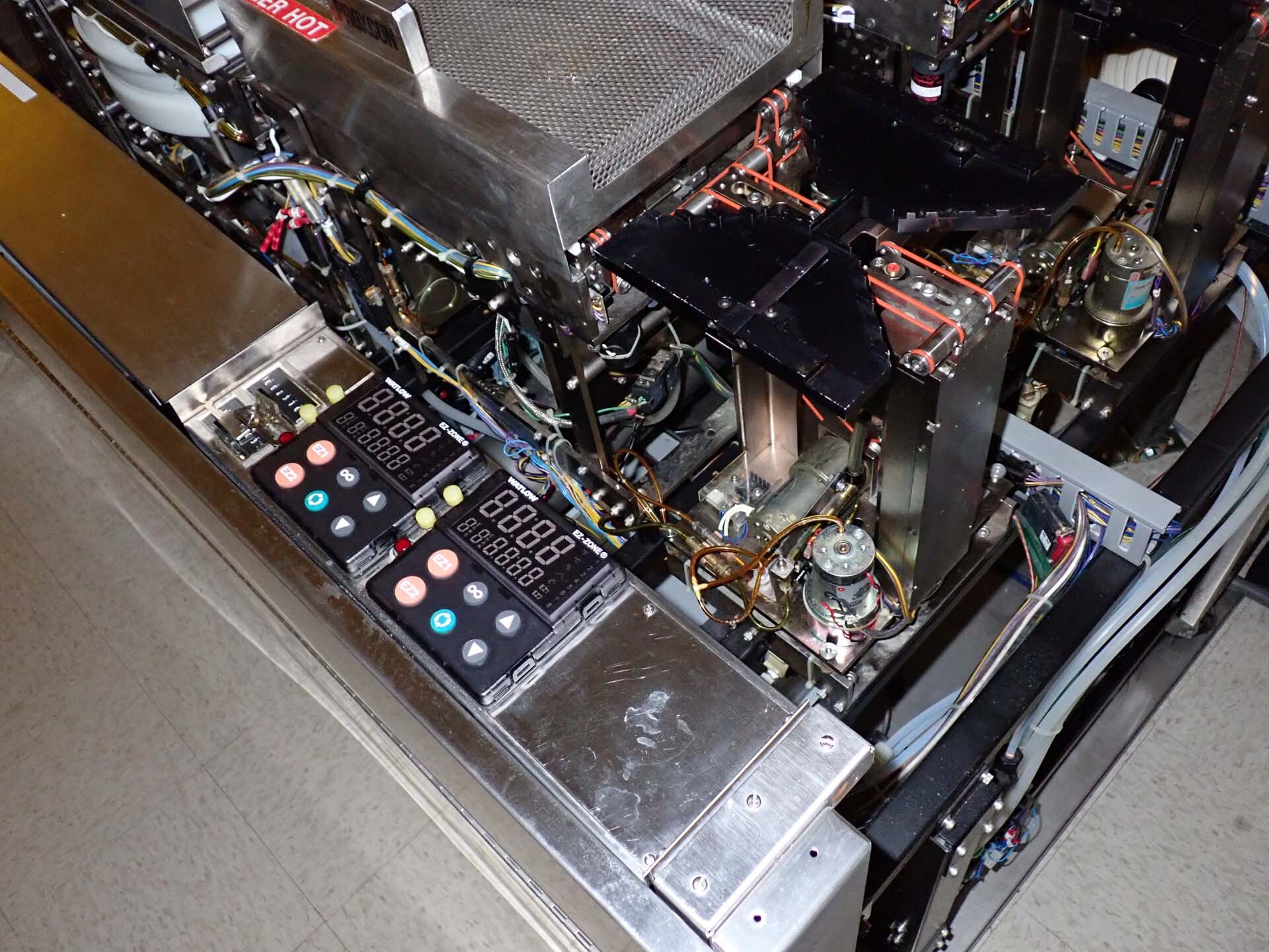
I'll provide a detailed description of SVG (3) Developer Systems, specifically focusing on the photoresist equipment, in 500 words. SVG (3) Developer Systems are advanced tools used in the semiconductor industry for the precise patterning of photoresist layers on wafers during the fabrication process. Photoresist plays a crucial role in photolithography, where a pattern is transferred onto a substrate to define the features of integrated circuits. SVG (3) Developer Systems are designed to ensure accurate and reproducible patterning, essential for achieving high-quality semiconductor devices with intricate circuit designs. The photoresist system within SVG (3) Developer is a critical component that enables the deposition, development, and removal of photoresist materials on semiconductor wafers. Photoresist serves as a light-sensitive material that undergoes chemical changes upon exposure to light, allowing for the transfer of patterns onto the wafer surface. The photoresist unit in an SVG (3) Developer consists of several key elements, including a photoresist dispenser, developer module, and rinse station. The photoresist dispenser in an SVG (3) Developer Machine is responsible for precisely dispensing the photoresist material onto the wafer surface. This process is crucial for achieving uniform and well-controlled coating thickness across the entire wafer. The dispenser tool is equipped with precision controls to adjust the flow rate, viscosity, and other parameters to ensure consistent and reliable photoresist deposition. Once the photoresist material is dispensed onto the wafer, it undergoes the development process in the developer module. The developer module contains chemical solutions that selectively dissolve either the exposed or unexposed regions of the photoresist layer, depending on the type of photoresist used (positive or negative). This step is critical for creating the desired pattern on the wafer surface with high fidelity and resolution. After the development process, the wafer undergoes a rinsing step in the rinse station to remove any residual photoresist and developer chemicals. Proper rinsing is essential to prevent contamination and ensure the cleanliness of the wafer surface before proceeding to subsequent processing steps in the semiconductor fabrication process. In addition to these primary components, the photoresist asset in an SVG (3) Developer also features advanced monitoring and control capabilities. Real-time monitoring of critical parameters such as temperature, pressure, flow rates, and chemical concentrations allows for precise control of the photoresist deposition and development processes. Automated feedback mechanisms enable adjustments to be made in real-time to maintain process stability and consistency. Furthermore, SVG (3) Developer Systems are designed to be highly flexible and modular, allowing for customization based on specific process requirements and wafer sizes. The photoresist model can be integrated seamlessly with other process modules within SVG (3) Developer platform to create a fully automated and integrated semiconductor fabrication line. Overall, SVG (3) Developer Systems with a photoresist equipment play a vital role in the production of advanced semiconductor devices by enabling precise patterning of photoresist layers with high accuracy and repeatability. These systems are indispensable tools for semiconductor manufacturers seeking to achieve cutting-edge technology nodes and produce complex integrated circuits with superior performance and reliability.
There are no reviews yet