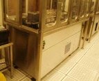
Used SVG 86 #9163180 for sale
URL successfully copied!
Tap to zoom
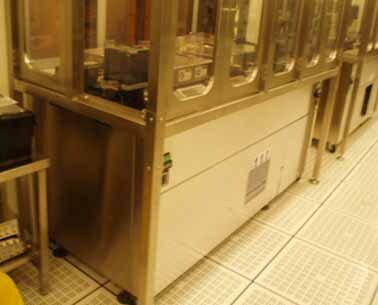

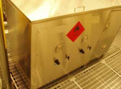

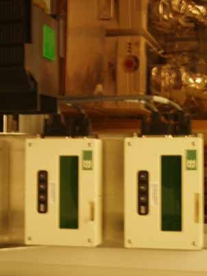

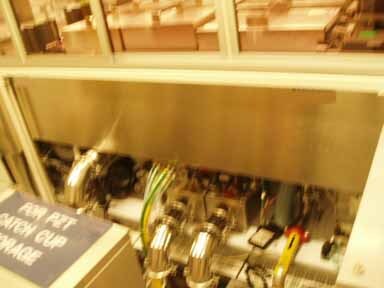

ID: 9163180
Wafer Size: 6"
Double coater, 6"
Semi flat wafers
Cassettes: Fluor ware
Coater wafer direction: Left to right
Coater with MYKROLIS IntelliGen 2 Pump
Coater exhaust with auto-damper
Hardware:
SMC Digital vacuum sensor
Coater bottom EBR with flow meter
Does not include:
Coater with catch-cup-rinse
Thru-track interface to pe micralign riro
MICROBAR chemical cabinet
CTD
CTR
Vacuum bake wafer prime
Coater spinner with servo pack
Coater dispense line with flow meter
Coater top EBR with flow meter
Coater catch-cup-rinse with flow meter
ADS Resist reservoir system
No automation
Power supply: 415 VAC, 3 Phase
2010 vintage.
SVG 86 is a photoresist equipment developed by Silicon Valley Group (SVG) for use in the semiconductor industry. It is a single-photo, flowable resist that provides excellent printing results, with reliable edge resolution and exposure latitude. The system consists of a photoresist material, an image mask, a photoresist developer solution, and a chemical treatment unit. In use, the photoresist material is applied to the surface of a semiconductor wafer and exposed to ultraviolet (UV) light from the image mask. The light causes certain portions of the resist to dissolve, while others remain intact. The remaining portions form the pattern that will be transferred onto the wafer. 86 is designed to produce high-resolution images with a consistent thickness of material and uniform edge resolution. It has a low light sensitivity, meaning that it can be exposed to high-intensity light while still producing a clean, precise image. The resist also has excellent chemical resistance properties, and is resistant to bleaching, corrosion, and etching. SVG 86 is used in many different semiconductor fabrication processes. It is used to create a range of components such as microelectromechanical systems (MEMS), microcontrollers, and integrated chipsets. It is also used in the production of photoresistors, thin-film transistors, and light-emitting diodes (LEDs). Additionally, it is used to pattern solar cells and photovoltaic cells. The machine is well suited for high-volume and high-precision fabrication. It is commonly used in the fabrication of advanced materials, such as strained silicon, germanium, compound semiconductors, and nanostructures. The tool is easy to use, and requires minimal operator training. 86 is designed to be an affordable photoresist solution that is suitable for a wide variety of semiconductor applications. It is highly reliable, with low defect rates and high yields. This makes it ideal for high-volume production, and enhances the reliability and performance of the finished device.
There are no reviews yet
